As of January 2026, the global artificial intelligence landscape has shifted from a race between corporate titans to a high-stakes competition between nation-states. Driven by the need for strategic autonomy and a desire to decouple from a volatile global supply chain, a new era of "Sovereign AI" has arrived. This movement is defined by massive government-backed initiatives designed to build domestic chip manufacturing, secure massive GPU clusters, and develop localized AI models that reflect national languages and values.
The significance of this trend cannot be overstated. By investing billions into domestic infrastructure, nations are effectively attempting to build "digital fortresses" that protect their economic and security interests. In just the last year, Japan, India, and Canada have emerged as the vanguard of this movement, committing tens of billions of dollars to ensure they are not merely consumers of AI developed in Silicon Valley or Beijing, but architects of their own technological destiny.
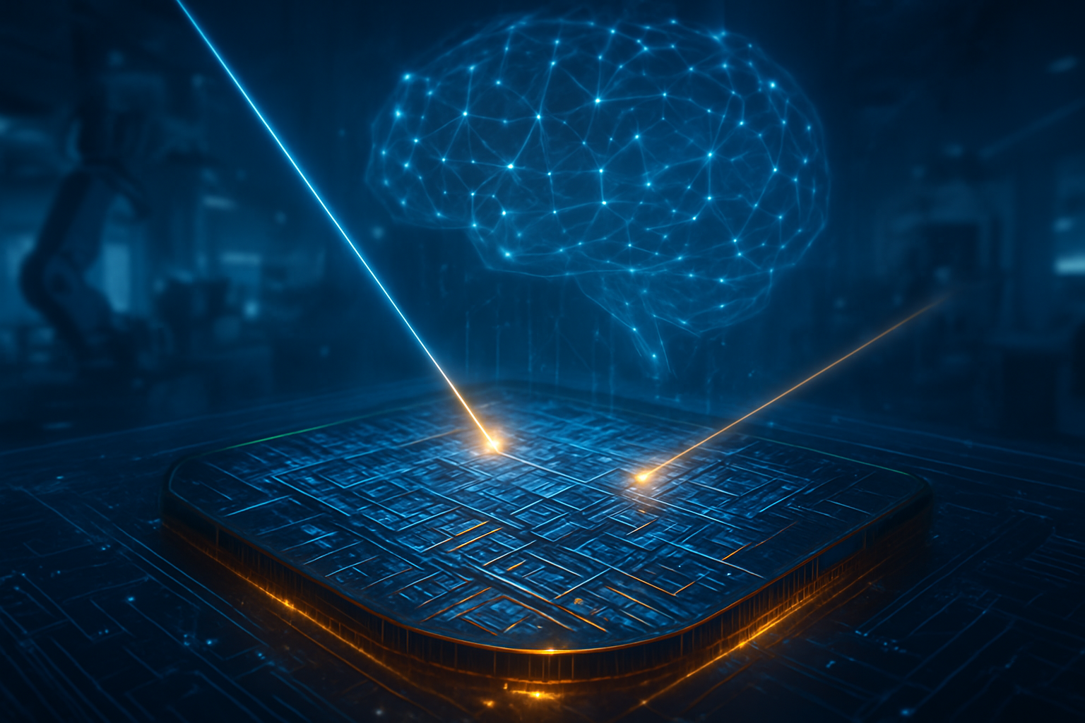
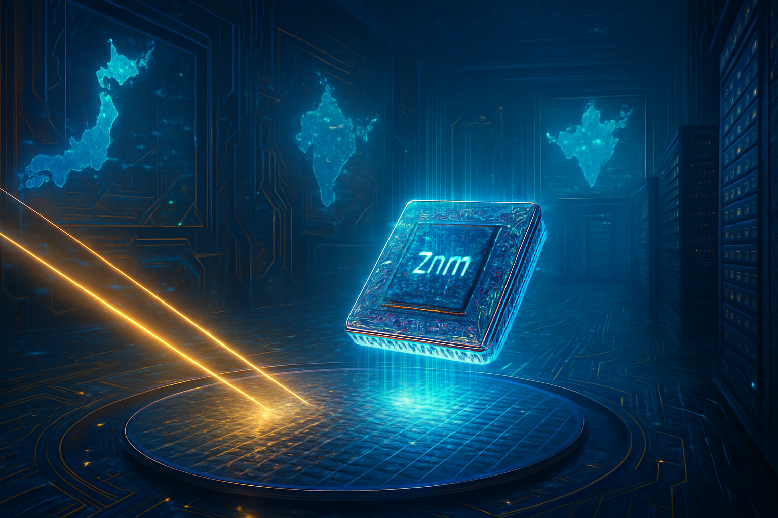
Breaking the 2nm Barrier and the Blackwell Revolution
At the technical heart of the Sovereign AI movement is a push for cutting-edge hardware and massive compute density. In Japan, the government has doubled down on its "Rapidus" project, approving a fresh ¥1 trillion ($7 billion USD) injection to achieve mass production of 2nm logic chips by 2027. To support this, Japan has successfully integrated the first ASML (NASDAQ: ASML) NXE:3800E EUV lithography systems at its Hokkaido facility, positioning itself as a primary competitor to TSMC and Intel (NASDAQ: INTC) in the sub-3nm era. Simultaneously, SoftBank (TYO: 9984) has partnered with NVIDIA (NASDAQ: NVDA) to deploy the "Grace Blackwell" GB200 platform, scaling Japan’s domestic compute power to over 25 exaflops—a level of processing power that was unthinkable for a private-public partnership just two years ago.
India’s approach combines semiconductor fabrication with a massive "population-scale" compute mission. The IndiaAI Mission has successfully sanctioned the procurement of over 34,000 GPUs, with 17,300 already operational across local data centers managed by partners like Yotta and Netmagic. Technically, India is pursuing a "full-stack" strategy: while Tata Electronics builds its $11 billion fab in Dholera to produce 28nm chips for edge-AI devices, the nation has also established itself as a global hub for 2nm chip design through a major new facility opened by Arm (NASDAQ: ARM). This allows India to design the world's most advanced silicon domestically, even while its manufacturing capabilities mature.
Canada has taken a unique path by focusing on public-sector AI infrastructure. Through its 2024 and 2025 budgets, the Canadian government has committed nearly $3 billion CAD to create a Sovereign Public AI Infrastructure. This includes the AI Sovereign Compute Infrastructure Program (SCIP), which aims to build a single, government-owned supercomputing facility that provides academia and SMEs with subsidized access to NVIDIA H200 and Blackwell chips. Furthermore, private Canadian firms like Hypertec have committed to reserving up to 50,000 GPUs for sovereign use, ensuring that Canadian data never leaves the country’s borders during the training or inference of sensitive public-sector models.
The Hardware Gold Rush and the Shift in Tech Power
The rise of Sovereign AI has created a new category of "must-win" customers for the world’s major tech companies. NVIDIA (NASDAQ: NVDA) has emerged as the primary beneficiary, effectively becoming the "arms dealer" for national governments. By tailoring its offerings to meet "sovereign" requirements—such as data residency and localized security protocols—NVIDIA has offset potential slowdowns in the commercial cloud sector with massive government contracts. Other hardware giants like IBM (NYSE: IBM), which is a key partner in Japan’s 2nm project, and specialized providers like Oracle (NYSE: ORCL), which provides sovereign cloud regions, are seeing their market positions strengthened as nations prioritize security over the lowest cost.
This shift presents a complex challenge for traditional "Big Tech" firms like Microsoft (NASDAQ: MSFT) and Alphabet (NASDAQ: GOOGL). While they remain dominant in AI services, the push for domestic infrastructure threatens their total control over the global AI stack. Startups in these "sovereign" nations are no longer solely dependent on Azure or AWS; they now have access to government-subsidized, locally-hosted compute power. This has paved the way for domestic champions like Canada's Cohere or India's Sarvam AI to build large-scale models that are optimized for local needs, creating a more fragmented—and arguably more competitive—global market.
Geopolitics, Data Privacy, and the Silicon Shield
The broader significance of the Sovereign AI movement lies in the transition from "software as a service" to "sovereignty as a service." For years, the AI landscape was a duopoly between the US and China. The emergence of Japan, India, and Canada as independent "compute powers" suggests a multi-polar future where digital sovereignty is as important as territorial integrity. By owning the silicon, the data centers, and the training data, these nations are building a "silicon shield" that protects them from external supply chain shocks or geopolitical pressure.
However, this trend also raises significant concerns regarding the "balkanization" of the internet and AI research. As nations build walled gardens for their AI ecosystems, the spirit of global open-source collaboration faces new hurdles. There is also the environmental impact of building dozens of massive new data centers globally, each requiring gigawatts of power. Comparisons are already being made to the nuclear arms race of the 20th century; the difference today is that the "deterrent" isn't a weapon, but the ability to process information faster and more accurately than one's neighbors.
The Road to 1nm and Indigenous Intelligence
Looking ahead, the next three to five years will see these initiatives move from the construction phase to the deployment phase. Japan is already eyeing the 1.4nm and 1nm nodes for 2030, aiming to reclaim its 1980s-era dominance in the semiconductor market. In India, the focus will shift toward "Indigenous LLMs"—models trained exclusively on Indian languages and cultural data—designed to bring AI services to hundreds of millions of citizens in their native tongues.
Experts predict that we will soon see the rise of "Regional Compute Hubs," where nations like Canada or Japan provide sovereign compute services to smaller neighboring countries, creating new digital alliances. The primary challenge will remain the talent war; building a multi-billion dollar data center is easier than training the thousands of specialized engineers required to run it. We expect to see more aggressive national talent-attraction policies, such as "AI Visas," as these countries strive to fill the high-tech roles created by their infrastructure investments.
Conclusion: A Turning Point in AI History
The rise of Sovereign AI marks a definitive end to the era of globalized, borderless technology. Japan’s move toward 2nm manufacturing, India’s massive GPU procurement, and Canada’s public supercomputing initiatives are the first chapters in a story of national self-reliance. The key takeaway for 2026 is that AI is no longer just a tool for productivity; it is the fundamental infrastructure of the modern state.
As we move into the middle of the decade, the success of these programs will determine which nations thrive in the automated economy. The significance of this development in AI history is comparable to the creation of the interstate highway system or the national power grid—it is the laying of the foundation for everything that comes next. In the coming weeks and months, the focus will shift to how these nations begin to utilize their newly minted "sovereign" power to regulate and deploy AI in ways that reflect their unique national identities.
This content is intended for informational purposes only and represents analysis of current AI developments.
TokenRing AI delivers enterprise-grade solutions for multi-agent AI workflow orchestration, AI-powered development tools, and seamless remote collaboration platforms.
For more information, visit https://www.tokenring.ai/.