Tag: AI Manufacturing

  • EU Chips Act 2.0: Strengthening Europe’s Path from Lab to Fab

    EU Chips Act 2.0: Strengthening Europe’s Path from Lab to Fab

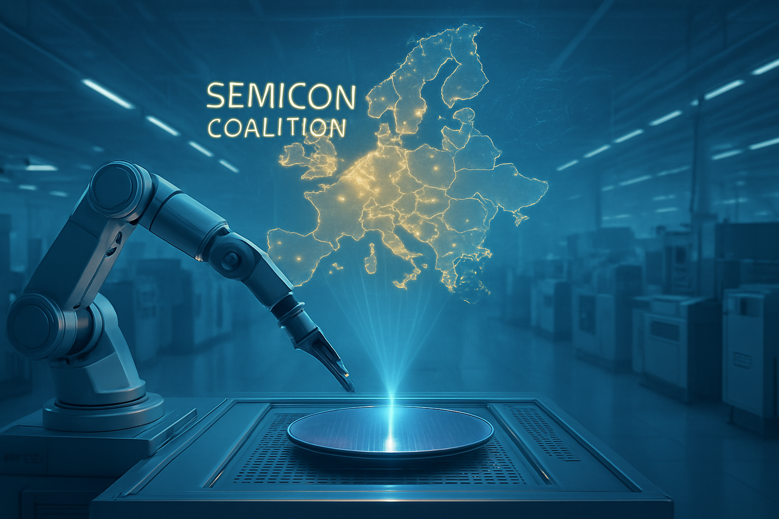
    As 2025 draws to a close, the European Union is signaling a massive strategic pivot in its quest for technological autonomy. Building on the foundation of the 2023 European Chips Act, the European Commission has officially laid the groundwork for "EU Chips Act 2.0." This "mid-course correction," as many Brussels insiders call it, aims to bridge the notorious "lab-to-fab" gap—the chasm between Europe's world-leading semiconductor research and its actual industrial manufacturing output. With a formal legislative proposal slated for the first quarter of 2026, the initiative represents a shift from a defensive posture to an assertive industrial policy designed to secure Europe’s place in the global AI hierarchy.

    The urgency behind Chips Act 2.0 is driven by a realization that while the original act catalyzed over €80 billion in private and public investment, the target of capturing 20% of the global semiconductor market by 2030 remains elusive. As of December 2024, the global race for AI supremacy has made advanced silicon more than just a commodity; it is now the bedrock of national security and economic resilience. By focusing on streamlined approvals and high-volume fabrication of advanced AI chips, the EU hopes to ensure that the next generation of generative AI models is not just designed in Europe, but powered by chips manufactured on European soil.

    Bridging the Chasm: The Technical Pillars of 2.0

    The centerpiece of the EU Chips Act 2.0 is the RESOLVE Initiative, a "lab-to-fab" accelerator launched in early 2025 that is now being formalized into law. Unlike previous efforts that focused broadly on capacity, RESOLVE targets 15 specific technology tracks, including 3D heterogeneous integration, advanced memory architectures, and sub-5nm logic. The goal is to create a seamless pipeline where innovations from world-renowned research centers like imec in Belgium, CEA-Leti in France, and Fraunhofer in Germany can be rapidly transitioned to industrial pilot lines and eventually high-volume manufacturing. This addresses a long-standing critique from the European Court of Auditors: that Europe too often "exports its brilliance" to be manufactured by competitors in Asia or the United States.

    A critical technical shift in the 2.0 framework is the emphasis on Advanced Packaging. Following recommendations from the updated 2025 "Draghi Report," the EU is prioritizing back-end manufacturing capabilities. As Moore’s Law slows down, the ability to stack chips (3D packaging) has become the primary driver of AI performance. The new legislation proposes a harmonized EU-wide permitting regime to bypass the fragmented national bureaucracies that have historically delayed fab construction. By treating semiconductor facilities as "projects of overriding public interest," the EU aims to move from project notification to groundbreaking in months rather than years, a pace necessary to compete with the rapid expansion seen in the U.S. and China.

    Initial reactions from the industry have been cautiously optimistic. Christophe Fouquet, CEO of ASML (NASDAQ: ASML), recently warned that without the faster execution promised by Chips Act 2.0, the EU risks losing its relevance in the global AI race. Similarly, industry lobbies like SEMI Europe have praised the focus on "Fast-Track IPCEIs" (Important Projects of Common European Interest), though they continue to warn against any additional administrative burdens or "sovereignty certifications" that could complicate global supply chains.

    The Corporate Landscape: Winners and Strategic Shifts

    The move toward Chips Act 2.0 creates a new set of winners in the European tech ecosystem. Traditional European powerhouses like Infineon Technologies (OTCMKTS: IFNNY), NXP Semiconductors (NASDAQ: NXPI), and STMicroelectronics (NYSE: STM) stand to benefit from increased subsidies for "Edge AI" and automotive silicon. However, the 2.0 framework also courts global giants like Intel (NASDAQ: INTC) and TSMC (NYSE: TSM). The EU's push for sub-5nm manufacturing is specifically designed to ensure that these firms continue their expansion in hubs like Magdeburg, Germany, and Dresden, providing the high-end logic chips required for training large-scale AI models.

    For major AI labs and startups, the implications are profound. Currently, European AI firms are heavily dependent on Nvidia (NASDAQ: NVDA) and U.S.-based cloud providers for compute resources. The "AI Continent Action Plan," a key component of the 2.0 strategy, aims to foster a domestic alternative. By subsidizing the design and manufacture of European-made high-performance computing (HPC) chips, the EU hopes to create a "sovereign compute" stack. This could potentially disrupt the market positioning of U.S. tech giants by offering European startups a localized, regulation-compliant infrastructure that avoids the complexities of transatlantic data transfers and export controls.

    Sovereignty in an Age of Geopolitical Friction

    The wider significance of Chips Act 2.0 cannot be overstated. It is a direct response to the weaponization of technology in global trade. Throughout 2025, heightened U.S. export restrictions and China’s facility-level export bans have highlighted the vulnerability of the European supply chain. The EU’s Tech Chief, Henna Virkkunen, has stated that the "top aim" is "indispensability"—creating a scenario where the world relies on European components (like ASML’s lithography machines) as much as Europe relies on external chips.

    This strategy mirrors previous AI milestones, such as the launch of the EuroHPC Joint Undertaking, but on a much larger industrial scale. However, concerns remain regarding the "funding gap." While the policy framework is robust, critics argue that the EU lacks the massive capital depth of the U.S. CHIPS and Science Act. The European Court of Auditors issued a sobering report in December 2025, suggesting that the 20% market share target is "very unlikely" without a significant increase in the central EU budget, beyond what member states can provide individually.

    The Horizon: What’s Next for European Silicon?

    In the near term, the industry is looking toward the official legislative rollout in Q1 2026. This will be the moment when the "lab-to-fab" vision meets the reality of budget negotiations. We can expect to see the first "Fast-Track" permits issued for advanced packaging facilities in late 2026, which will serve as a litmus test for the new harmonized permitting regime. On the applications front, the focus will likely shift toward "Green AI"—chips designed specifically for energy-efficient inference, leveraging Europe’s leadership in power semiconductors to carve out a niche in the global market.

    Challenges remain, particularly in workforce development. To run the advanced fabs envisioned in Chips Act 2.0, Europe needs tens of thousands of specialized engineers. Experts predict that the next phase of the policy will involve aggressive "talent visas" and massive investments in university-led semiconductor programs to ensure the "lab" side of the equation remains populated with the world’s best minds.

    A New Chapter for the Digital Decade

    The transition to EU Chips Act 2.0 marks a pivotal moment in European industrial history. It represents a move away from the fragmented, nation-state approach of the past toward a unified, pan-European strategy for the AI era. By focusing on the "lab-to-fab" pipeline and speeding up the bureaucratic machinery, the EU is attempting to prove that a democratic bloc can move with the speed and scale required by the modern technology landscape.

    As we move into 2026, the success of this initiative will be measured not just in euros spent, but in the number of high-end AI chips that roll off European assembly lines. The goal is clear: to ensure that when the history of the AI revolution is written, Europe is a primary author, not just a reader.


    This content is intended for informational purposes only and represents analysis of current AI developments.

    TokenRing AI delivers enterprise-grade solutions for multi-agent AI workflow orchestration, AI-powered development tools, and seamless remote collaboration platforms.
    For more information, visit https://www.tokenring.ai/.

  • Silicon Sovereignty: Tata and ROHM Forge Strategic Alliance to Power India’s Semiconductor Revolution

    Silicon Sovereignty: Tata and ROHM Forge Strategic Alliance to Power India’s Semiconductor Revolution

    In a landmark development for the global electronics supply chain, Tata Electronics has officially entered into a strategic partnership with Japan’s ROHM Co., Ltd. (TYO: 6963) to manufacture power semiconductors in India. Announced today, December 22, 2025, this collaboration marks a pivotal moment in India’s ambitious journey to transition from a software-centric economy to a global hardware and semiconductor manufacturing powerhouse. The deal focuses on the joint development and production of high-efficiency power devices, specifically targeting the burgeoning electric vehicle (EV) and industrial automation sectors.

    This partnership is not merely a bilateral agreement; it is the cornerstone of India’s broader strategy to secure its technological sovereignty. By integrating ROHM’s world-class expertise in wide-bandgap semiconductors with the massive industrial scale of the Tata Group, India is positioning itself to capture a significant share of the $80 billion global power semiconductor market. The move is expected to drastically reduce the nation’s reliance on imported silicon components, providing a stable, domestic supply chain for Indian automotive giants like Tata Motors (NSE: TATAMOTORS) and green energy leaders like Tata Power (NSE: TATAPOWER).

    Technical Breakthroughs: Silicon Carbide and the Future of Power Efficiency

    The technical core of the Tata-ROHM alliance centers on the manufacturing of advanced power discrete components. Initially, the partnership will focus on the assembly and testing of automotive-grade Silicon (Si) MOSFETs—specifically the Nch 100V, 300A variants—designed for high-current applications in electric drivetrains. However, the true disruptive potential lies in the roadmap for "Wide-Bandgap" (WBG) materials, including Silicon Carbide (SiC) and Gallium Nitride (GaN). Unlike traditional silicon, SiC and GaN allow for higher voltage operation, faster switching speeds, and significantly better thermal management, which are essential for extending the range and reducing the charging times of modern EVs.

    This collaboration differs from previous semiconductor initiatives in India by focusing on the "power" segment rather than just logic chips. Power semiconductors are the "muscles" of electronic systems, managing how electricity is converted and distributed. By establishing a dedicated production line for these components at Tata’s new Outsourced Semiconductor Assembly and Test (OSAT) facility in Jagiroad, Assam, the partnership ensures that India can produce chips that are up to 50% more efficient than current standards. Industry experts have lauded the move, noting that ROHM’s proprietary SiC technology is among the most advanced in the world, and its transfer to Indian soil represents a major leap in domestic technical capability.

    Market Disruption: Shifting the Global Semiconductor Balance of Power

    The strategic implications for the global tech landscape are profound. For years, the semiconductor industry has been heavily concentrated in East Asia, leaving global markets vulnerable to geopolitical tensions and supply chain bottlenecks. The Tata-ROHM partnership, backed by the Indian government’s $10 billion India Semiconductor Mission (ISM), provides a viable "China Plus One" alternative for global OEMs. Major tech giants and automotive manufacturers seeking to diversify their sourcing will now look toward India as a high-tech manufacturing hub that offers both scale and competitive cost structures.

    Within India, the primary beneficiaries will be the domestic EV ecosystem. Tata Motors (NSE: TATAMOTORS), which currently dominates the Indian electric car market, will gain a first-mover advantage by integrating locally-produced, high-efficiency chips into its future vehicle platforms. Furthermore, the partnership poses a competitive challenge to established European and American power semiconductor firms. By leveraging India’s lower operational costs and ROHM’s engineering prowess, the Tata-ROHM venture could potentially disrupt the pricing models for power modules globally, forcing competitors to accelerate their own investments in emerging markets.

    A National Milestone: India’s Transition to a Global Chip Hub

    This announcement fits into a broader trend of "techno-nationalism," where nations are racing to build domestic chip capabilities to ensure economic and national security. The Tata-ROHM deal is the latest in a series of high-profile successes for the India Semiconductor Mission. It follows the massive ₹91,000 crore investment in the Dholera mega-fab, a joint venture between Tata Electronics and Powerchip Semiconductor Manufacturing Corp (TPE: 6770), and the entry of Micron Technology (NASDAQ: MU) into the Indian packaging space. Together, these projects signal that India has moved past the "planning" phase and is now in the "execution" phase of its semiconductor roadmap.

    However, the rapid expansion is not without its challenges. The industry remains concerned about the availability of specialized ultra-pure water and uninterrupted high-voltage power—critical requirements for semiconductor fabrication. Comparisons are already being made to the early days of China’s semiconductor rise, with analysts noting that India’s democratic framework and strong intellectual property protections may offer a more stable long-term environment for international partners. The success of the Tata-ROHM partnership will serve as a litmus test for whether India can successfully manage the complex logistics of high-tech manufacturing at scale.

    The Road Ahead: 2026 and the Leap Toward "Semicon 2.0"

    Looking toward 2026, the partnership is expected to move into full-scale mass production. The Jagiroad facility in Assam is projected to reach a daily output of 48 million chips by early next year, while the Dholera fab will begin pilot runs for 28nm logic chips. The next frontier for the Tata-ROHM collaboration will be the integration of Artificial Intelligence (AI) into the manufacturing process. AI-driven predictive maintenance and yield optimization are expected to be implemented at the Dholera plant, making it one of the most advanced "Smart Fabs" in the world.

    Beyond manufacturing, the Indian government is already preparing for "Semicon 2.0," a second phase of incentives that will likely double the current financial outlay to $20 billion. This phase will focus on the upstream supply chain, including specialized chemicals, gases, and wafer production. Experts predict that if the current momentum continues, India could account for nearly 10% of the global semiconductor assembly and testing market by 2030, fundamentally altering the geography of the digital age.

    Conclusion: A New Era for Indian Electronics

    The partnership between Tata Electronics and ROHM Co., Ltd. is more than a business deal; it is a declaration of intent. It signifies that India is no longer content with being the world’s back-office for software but is ready to build the physical foundations of the future. By securing a foothold in the critical power semiconductor market, India is ensuring that its transition to a green, electrified economy is built on a foundation of domestic innovation and manufacturing.

    As we move into 2026, the world will be watching the progress of the Jagiroad and Dholera facilities with intense interest. The success of these projects will determine whether India can truly become the "third pillar" of the global semiconductor industry, alongside East Asia and the West. For now, the Tata-ROHM alliance stands as a testament to the power of international collaboration in solving the world's most complex technological challenges.


    This content is intended for informational purposes only and represents analysis of current AI and semiconductor developments as of December 22, 2025.

    TokenRing AI delivers enterprise-grade solutions for multi-agent AI workflow orchestration, AI-powered development tools, and seamless remote collaboration platforms.
    For more information, visit https://www.tokenring.ai/.
  • The Green Paradox: Can the AI Boom Survive the Semiconductor Industry’s Rising Resource Demands?

    The Green Paradox: Can the AI Boom Survive the Semiconductor Industry’s Rising Resource Demands?

    As of December 19, 2025, the global technology sector is grappling with a profound "green paradox." While artificial intelligence is being hailed as a critical tool for solving climate change, the physical manufacturing of the chips that power it—such as Nvidia’s Blackwell and Blackwell Ultra architectures—has pushed the semiconductor industry’s energy and water consumption to unprecedented levels. This week, industry leaders and environmental regulators have signaled a major pivot toward "Sustainable Silicon," as the resource-heavy requirements of 3nm and 2nm fabrication nodes begin to clash with global net-zero commitments.

    The immediate significance of this shift cannot be overstated. With the AI chip market continuing its meteoric rise, the environmental footprint of a single leading-edge wafer has nearly tripled compared to a decade ago. This has forced the world's largest chipmakers to adopt radical new technologies, from AI-driven "Digital Twin" factories to closed-loop water recycling systems, in an effort to decouple industrial growth from environmental degradation.

    Engineering the Closed-Loop Fab: Technical Breakthroughs in 2025

    The technical challenge of modern chip fabrication lies in the extreme complexity of the latest manufacturing nodes. As companies like TSMC (NYSE: TSM) and Samsung (KRX: 005930) move toward 2nm production, the number of mask layers and chemical processing steps has increased significantly. To combat the resulting resource drain, the industry has turned to "Counterflow Reverse Osmosis," a breakthrough in Ultra Pure Water (UPW) management. This technology now allows fabs to recycle up to 90% of their wastewater directly back into the sensitive wafer-rinsing stages—a feat previously thought impossible due to the risk of microscopic contamination.

    Energy consumption remains the industry's largest hurdle, primarily driven by Extreme Ultraviolet (EUV) lithography tools manufactured by ASML (NASDAQ: ASML). These machines, which are essential for printing the world's most advanced transistors, consume roughly 1.4 megawatts of power each. To mitigate this, TSMC has fully deployed its "EUV Dynamic Power Saving" program this year. By using real-time AI to pulse the EUV light source only when necessary, the system has successfully reduced tool-level energy consumption by 8% without sacrificing throughput.

    Furthermore, the industry is seeing a surge in AI-driven yield optimization. By utilizing deep learning for defect detection, manufacturers have reported a 40% reduction in defect rates on 3nm lines. This efficiency is a sustainability win: by catching errors early, fabs prevent the "waste" of thousands of gallons of UPW and hundreds of kilowatts of energy that would otherwise be spent processing a defective wafer. Industry experts have praised these advancements, noting that the "Intelligence-to-Efficiency" loop is finally closing, where AI chips are being used to optimize the very factories that produce them.

    The Competitive Landscape: Tech Giants Race for 'Green' Dominance

    The push for sustainability is rapidly becoming a competitive differentiator for the world's leading foundries and integrated device manufacturers. Intel (NASDAQ: INTC) has emerged as an early leader in renewable energy adoption, announcing this month that it has achieved 98% global renewable electricity usage. Intel’s "Net Positive Water" goal is also ahead of schedule, with its facilities in the United States and India already restoring more water to local ecosystems than they consume. This positioning is a strategic advantage as cloud providers seek to lower their Scope 3 emissions.

    For Nvidia (NASDAQ: NVDA), the sustainability of the fabrication process is now a core component of its market positioning. As the primary customer for TSMC’s most advanced nodes, Nvidia is under pressure from its own enterprise clients to provide "Green AI" solutions. The massive die size of Nvidia's Blackwell GPUs means fewer chips can be harvested from a single wafer, making each chip more "resource-expensive" than a standard mobile processor. In response, Nvidia has partnered with Samsung to develop Digital Twins of entire fabrication plants, using over 50,000 GPUs to simulate and optimize airflow and power loads, improving overall operational efficiency by an estimated 20%.

    This shift is also disrupting the supply chain for equipment manufacturers like Applied Materials (NASDAQ: AMAT) and Lam Research (NASDAQ: LRCX). There is a growing demand for "dry" lithography and etching solutions that eliminate the need for water-intensive processes. Startups focusing on sustainable chemistry are also finding new opportunities as the industry moves away from "forever chemicals" (PFAS) in response to tightening global regulations.

    The Regulatory Hammer and the Broader AI Landscape

    The broader significance of these developments is underscored by a new wave of international regulations. As of November 2024, the Global Electronics Council introduced stricter EPEAT criteria for semiconductors, and in 2025, the European Union's "Digital Product Passport" (DPP) became a mandatory requirement for chips sold in the region. This regulation forces manufacturers to provide a transparent "cradle-to-gate" account of the carbon and water footprint for every chip, effectively making sustainability a prerequisite for market access in Europe.

    This regulatory environment marks a departure from previous AI milestones, where the focus was almost entirely on performance and "flops per watt." Today, the conversation has shifted to the "embedded" environmental cost of the hardware itself. Concerns are mounting that the resource intensity of AI could lead to localized water shortages or energy grid instability in semiconductor hubs like Arizona, Taiwan, and South Korea. This has led to a comparison with the early days of data center expansion, but at a much more concentrated and resource-intensive scale.

    The Semiconductor Climate Consortium (SCC) has also launched a standardized Scope 3 reporting framework this year. This compels fabs to account for the carbon footprint of their entire supply chain, from raw silicon mining to the production of specialty gases. By standardizing these metrics, the industry is moving toward a future where "green silicon" could eventually command a price premium over traditionally manufactured chips.

    Looking Ahead: The Road to 2nm and Circularity

    In the near term, the industry is bracing for the transition to 2nm nodes, which is expected to begin in earnest in late 2026. While these nodes promise greater energy efficiency for the end-user, the fabrication process will be the most resource-intensive in history. Experts predict that the next major breakthrough will involve a move toward a "circular economy" for semiconductors, where rare-earth metals and silicon are reclaimed from decommissioned AI servers and fed back into the manufacturing loop.

    Potential applications on the horizon include the integration of small-scale modular nuclear reactors (SMRs) directly into fab campuses to provide a stable, carbon-free baseload of energy. Challenges remain, particularly in the elimination of PFAS, as many of the chemical substitutes currently under testing have yet to match the precision required for leading-edge nodes. However, the trajectory is clear: the semiconductor industry is moving toward a "Zero-Waste" model that treats water and energy as finite, precious resources rather than cheap industrial inputs.

    A New Era for Sustainable Computing

    The push for sustainability in semiconductor manufacturing represents a pivotal moment in the history of computing. The key takeaway from 2025 is that the AI revolution cannot be sustained by 20th-century industrial practices. The industry’s ability to innovate its way out of the "green paradox"—using AI to optimize the fabrication of AI—will determine the long-term viability of the current technological boom.

    As we look toward 2026, the industry's success will be measured not just by transistor density or clock speeds, but by gallons of water saved and carbon tons avoided. The shift toward transparent reporting and closed-loop manufacturing is a necessary evolution for a sector that has become the backbone of the global economy. Investors and consumers alike should watch for the first "Water-Positive" fab certifications and the potential for a "Green Silicon" labeling system to emerge in the coming months.


    This content is intended for informational purposes only and represents analysis of current AI developments.

    TokenRing AI delivers enterprise-grade solutions for multi-agent AI workflow orchestration, AI-powered development tools, and seamless remote collaboration platforms.
    For more information, visit https://www.tokenring.ai/.

  • The Green Paradox: How Semiconductor Giants are Racing to Decarbonize the AI Boom

    The Green Paradox: How Semiconductor Giants are Racing to Decarbonize the AI Boom

    As the calendar turns to late 2025, the semiconductor industry finds itself at a historic crossroads. The global insatiable demand for high-performance AI hardware has triggered an unprecedented manufacturing expansion, yet this growth is colliding head-on with the most ambitious sustainability targets in industrial history. Major foundries are now forced to navigate a "green paradox": while the chips they produce are becoming more energy-efficient, the sheer scale of production required to power the world’s generative AI models is driving absolute energy and water consumption to record highs.

    To meet this challenge, the industry's titans—Taiwan Semiconductor Manufacturing Co. (NYSE:TSM), Intel (Nasdaq:INTC), and Samsung Electronics (KRX:005930)—have moved beyond mere corporate social responsibility. In 2025, sustainability has become a core competitive metric, as vital as transistor density or clock speed. From massive industrial water reclamation plants in the Arizona desert to AI-driven "digital twin" factories in South Korea, the race is on to prove that the silicon backbone of the future can be both high-performance and environmentally sustainable.

    The High-NA Energy Trade-off and Technical Innovations

    The technical centerpiece of 2025's manufacturing landscape is the High-NA (High Numerical Aperture) EUV lithography system, primarily supplied by ASML (Nasdaq:ASML). These machines, such as the EXE:5200 series, are the most complex tools ever built, but they come with a significant environmental footprint. A single High-NA EUV tool now consumes approximately 1.4 Megawatts (MW) of power—a 20% increase over standard EUV systems. However, foundries argue that this is a net win for sustainability. By enabling "single-exposure" lithography for the 2nm and 1.4nm nodes, these tools eliminate the need for 3–4 multi-patterning steps required by older machines, effectively saving an estimated 200 kWh per wafer produced.

    Beyond lithography, water management has seen a radical technical overhaul. TSMC (NYSE:TSM) recently reached a major milestone with the groundbreaking of its Arizona Industrial Reclamation Water Plant (IRWP). This 15-acre facility is designed to achieve a 90% water recycling rate for its US operations by 2028. Similarly, in Taiwan, the Rende Reclaimed Water Plant became fully operational this year, providing a critical lifeline to the Tainan Science Park’s 3nm and 2nm lines. These facilities use advanced membrane bioreactors and reverse osmosis systems to ensure that every gallon of water is reused multiple times before being safely returned to the environment.

    Samsung (KRX:005930) has taken a different technical route by applying AI to the manufacturing of AI chips. In a landmark partnership with NVIDIA (Nasdaq:NVDA), Samsung has deployed "Digital Twin" technology across its Hwaseong and Pyeongtaek campuses. By creating a real-time virtual replica of the entire fab, Samsung uses over 50,000 GPUs to simulate and optimize airflow, chemical distribution, and power consumption. Early data from late 2025 suggests this AI-driven management has improved operational energy efficiency by nearly 20 times compared to legacy manual systems, demonstrating a circular logic where AI is the primary tool used to mitigate its own environmental impact.

    Market Positioning: The Rise of the "Sustainable Foundry"

    Sustainability has shifted from a line item in an annual report to a strategic advantage in foundry contract negotiations. Intel (Nasdaq:INTC) has positioned itself as the industry's sustainability leader, marketing its "Intel 18A" node not just on performance, but as the world’s most "sustainable advanced node." By late 2025, Intel maintained a 99% renewable electricity rate across its global operations and achieved a "Net Positive Water" status in key regions like Oregon, where it has restored over 10 billion cumulative gallons to local watersheds. This allows Intel to pitch itself to climate-conscious tech giants who are under pressure to reduce their Scope 3 emissions.

    The competitive implications are stark. As cloud providers like Microsoft, Google, and Amazon strive for carbon neutrality, they are increasingly scrutinizing the carbon footprint of the chips in their data centers. TSMC (NYSE:TSM) has responded by accelerating its RE100 timeline, now aiming for 100% renewable energy by 2040—a full decade ahead of its original 2050 target. TSMC is also leveraging its market dominance to enforce "Green Agreements" with over 50 of its tier-1 suppliers, essentially mandating carbon reductions across the entire semiconductor supply chain to ensure its chips remain the preferred choice for the world’s largest tech companies.

    For startups and smaller AI labs, this shift is creating a new hierarchy of hardware. "Green Silicon" is becoming a premium tier of the market. While the initial CapEx for these sustainable fabs is enormous—with the industry spending over $160 billion in 2025 alone—the long-term operational savings from reduced water and energy waste are expected to stabilize chip prices in an era of rising resource costs. Companies that fail to adapt to these ESG requirements risk being locked out of high-value government contracts and the supply chains of the world’s largest consumer electronics brands.

    Global Significance and the Path to Net-Zero

    The broader significance of these developments cannot be overstated. The semiconductor industry's energy transition is a microcosm of the global challenge to decarbonize heavy industry. In Taiwan, TSMC’s energy footprint is projected to account for 12.5% of the island’s total power consumption by the end of 2025. This has turned semiconductor sustainability into a matter of national security and regional stability. The ability of foundries to integrate massive amounts of renewable energy—often through dedicated offshore wind farms and solar arrays—is now a prerequisite for obtaining the permits needed to build new multi-billion dollar "mega-fabs."

    However, concerns remain regarding the "carbon spike" associated with the construction of these new facilities. While the operational phase of a fab is becoming greener, the embodied carbon in the concrete, steel, and advanced machinery required for 18 new major fab projects globally in 2025 is substantial. Industry experts are closely watching whether the efficiency gains of the 2nm and 1.4nm nodes will be enough to offset the sheer volume of production. If AI demand continues its exponential trajectory, even a 90% recycling rate may not be enough to prevent a net increase in resource withdrawal.

    Comparatively, this era represents a shift from "Scaling at any Cost" to "Responsible Scaling." Much like the transition from leaded to unleaded gasoline or the adoption of scrubbers in the shipping industry, the semiconductor world is undergoing a fundamental re-engineering of its core processes. The move toward a "Circular Economy"—where Samsung (KRX:005930) now uses 31% recycled plastic in its components and all major foundries upcycle over 60% of their manufacturing waste—marks a transition toward a more mature, resilient industrial base.

    Future Horizons: The Road to 14A and Beyond

    Looking ahead to 2026 and beyond, the industry is already preparing for the next leap in sustainable manufacturing. Intel’s (Nasdaq:INTC) 14A roadmap and TSMC’s (NYSE:TSM) A16 node are being designed with "sustainability-first" architectures. This includes the wider adoption of Backside Power Delivery, which not only improves performance but also reduces the energy lost as heat within the chip itself. We also expect to see the first "Zero-Waste" fabs, where nearly 100% of chemicals and water are processed and reused on-site, effectively decoupling semiconductor production from local environmental constraints.

    The next frontier will be the integration of small-scale nuclear power, specifically Small Modular Reactors (SMRs), to provide consistent, carbon-free baseload power to mega-fabs. While still in the pilot phase in late 2025, several foundries have begun feasibility studies to co-locate SMRs with their newest manufacturing hubs. Challenges remain, particularly in the decarbonization of the "last mile" of the supply chain and the sourcing of rare earth minerals, but the momentum toward a truly green silicon shield is now irreversible.

    Summary and Final Thoughts

    The semiconductor industry’s journey in 2025 has proven that environmental stewardship and technological advancement are no longer mutually exclusive. Through massive investments in water reclamation, the adoption of High-NA EUV for process efficiency, and the use of AI to optimize the very factories that create it, the world's leading foundries are setting a new standard for industrial sustainability.

    Key takeaways from this year include:

    • Intel (Nasdaq:INTC) leading on renewable energy and water restoration.
    • TSMC (NYSE:TSM) accelerating its RE100 goals to 2040 to meet client demand.
    • Samsung (KRX:005930) pioneering AI-driven digital twins to slash operational waste.
    • ASML (Nasdaq:ASML) providing the High-NA tools that, while power-hungry, simplify manufacturing to save energy per wafer.

    In the coming months, watch for the first production yields from the 2nm nodes and the subsequent environmental audits. These reports will be the ultimate litmus test for whether the "Green Paradox" has been solved or if the AI boom will require even more radical interventions to protect our planet's resources.


    This content is intended for informational purposes only and represents analysis of current AI developments.

    TokenRing AI delivers enterprise-grade solutions for multi-agent AI workflow orchestration, AI-powered development tools, and seamless remote collaboration platforms.
    For more information, visit https://www.tokenring.ai/.

  • The Silicon Bloom: How ‘Green Chip’ Manufacturing is Redefining the AI Era’s Environmental Footprint

    The Silicon Bloom: How ‘Green Chip’ Manufacturing is Redefining the AI Era’s Environmental Footprint

    As the global demand for artificial intelligence reaches a fever pitch in late 2025, the semiconductor industry is undergoing its most significant transformation since the invention of the integrated circuit. The era of "performance at any cost" has officially ended, replaced by a mandate for "Green Chip" manufacturing. Major foundries are now racing to decouple the exponential growth of AI compute from its environmental impact, deploying radical new technologies in water reclamation and chemical engineering to meet aggressive Net Zero targets.

    This shift is not merely a corporate social responsibility initiative; it is a fundamental survival strategy. With the European Union’s August 2025 updated PFAS restriction proposal and the rising cost of water in chip-making hubs like Arizona and Taiwan, sustainability has become the new benchmark for competitive advantage. The industry’s leaders are now proving that the same AI chips that consume massive amounts of energy during production are the very tools required to optimize the world’s most complex manufacturing facilities.

    Technical Breakthroughs: The End of 'Forever Chemicals' and the Rise of ZLD

    At the heart of the "Green Chip" movement is a total overhaul of the photolithography process, which has historically relied on per- and polyfluoroalkyl substances (PFAS), known as "forever chemicals." As of late 2025, a major breakthrough has emerged in the form of Metal-Oxide Resists (MORs). Developed in collaboration between Imec and industry leaders, these tin-oxide-based resists are inherently PFAS-free. Unlike traditional chemically amplified resists (CAR) that use PFAS-based photoacid generators, MORs offer superior resolution for the 2nm and 1.4nm nodes currently entering high-volume manufacturing. This transition represents a technical pivot that many experts thought impossible just three years ago.

    Beyond chemistry, the physical infrastructure of the modern "Mega-Fab" has evolved into a closed-loop ecosystem. New facilities commissioned in 2025 by Intel Corporation (NASDAQ: INTC) and Taiwan Semiconductor Manufacturing Co. (TPE: 2330 / NYSE: TSM) are increasingly adopting Zero Liquid Discharge (ZLD) technologies. These systems utilize advanced thermal desalination and AI-driven "Digital Twins" to monitor water purity in real-time, allowing foundries to recycle nearly 100% of their process water on-site. Furthermore, the introduction of graphene-based filtration membranes in April 2025 has allowed foundries to strip 99.9% of small-chain PFAS molecules from wastewater, preventing environmental contamination before it leaves the plant.

    These advancements differ from previous "green-washing" efforts by being baked into the core transistor fabrication process. Previous approaches focused on downstream carbon offsets; the 2025 model focuses on upstream process elimination. Initial reactions from the research community have been overwhelmingly positive, with the Journal of Colloid and Interface Science noting that the replication of fluorine’s "bulkiness" using non-toxic carbon-hydrogen groups is a landmark achievement in sustainable chemistry that could have implications far beyond semiconductors.

    The Competitive Landscape: Who Wins in the Green Foundry Race?

    The transition to sustainable manufacturing is creating a new hierarchy among chipmakers. TSMC has reached a critical milestone in late 2025, declaring this the year of "Carbon Peak." By committing to the Science Based Targets initiative (SBTi) and mandating that 90% of its supply chain reach 85% renewable energy by 2030, TSMC is using its market dominance to force a "green" standard across the globe. This strategic positioning makes them the preferred partner for "Big Tech" firms like Apple and Nvidia, who are under immense pressure to reduce their Scope 3 emissions.

    Intel has carved out a leadership position in water stewardship, achieving "Water Net Positive" status in five countries as of December 2025. Their ability to operate in water-stressed regions like Arizona and Poland without depleting local aquifers provides a massive strategic advantage in securing government permits and subsidies. Meanwhile, Samsung Electronics (KRX: 005930) has focused on "Zero Waste-to-Landfill" certifications, with all of its global semiconductor sites achieving Platinum status this year. This focus on circularity is particularly beneficial for their memory division, as the high-volume production of HBM4 (High Bandwidth Memory) requires massive material throughput.

    The disruption to existing products is significant. Companies that fail to transition away from PFAS-reliant processes face potential exclusion from the European market and higher insurance premiums. Major lithography provider ASML (NASDAQ: ASML) has also had to adapt, ensuring their latest High-NA EUV machines are compatible with the new PFAS-free metal-oxide resists. This has created a "moat" for companies with the R&D budget to redesign their chemistry stacks, potentially leaving smaller, legacy-focused foundries at a disadvantage.

    The AI Paradox: Solving the Footprint with the Product

    The wider significance of this shift lies in what experts call the "AI Sustainability Paradox." The surge in AI chip production has driven an 8-12% annual increase in sector-wide energy usage through 2025. However, AI is also the primary tool being used to mitigate this footprint. For example, TSMC’s AI-optimized chiller systems saved an estimated 100 million kWh of electricity this year alone. This creates a feedback loop where more efficient AI chips lead to more efficient manufacturing, which in turn allows for the production of even more advanced chips.

    Regulatory pressure has been the primary catalyst for this change. The EU’s 2025 PFAS restrictions have moved from theoretical debates to enforceable law, forcing the industry to innovate at a pace rarely seen outside of Moore's Law. This mirrors previous industry milestones, such as the transition to lead-free soldering (RoHS) in the early 2000s, but on a much more complex and critical scale. The move toward "Green Chips" is now viewed as a prerequisite for the continued social license to operate in an era of climate volatility.

    However, concerns remain. While Scopes 1 and 2 (direct and indirect energy) are being addressed through renewable energy contracts, Scope 3 (the supply chain) remains a massive hurdle. The mining of raw materials for these "green" processes—such as the tin required for MORs—carries its own environmental and ethical baggage. The industry is effectively solving one chemical persistence problem while potentially increasing its reliance on other rare-earth minerals.

    Future Outlook: Bio-Based Chemicals and 100% Renewable Fabs

    Looking ahead, the next frontier in green chip manufacturing will likely involve bio-based industrial chemicals. Research into "engineered microbes" capable of synthesizing high-purity solvents for wafer cleaning is already underway, with pilot programs expected in 2027. Experts predict that by 2030, the "Zero-Emission Fab" will become the industry standard for all new 1nm-class construction, featuring on-site hydrogen power generation and fully autonomous waste-sorting systems.

    The immediate challenge remains the scaling of these technologies. While 2nm nodes can use PFAS-free MORs, the transition for older "legacy" nodes (28nm and above) is much slower due to the thin margins and aging equipment in those facilities. We can expect a "two-tier" market to emerge: premium "Green Chips" for high-end AI and consumer electronics, and legacy chips that face increasing regulatory taxes and environmental scrutiny.

    In the coming months, the industry will be watching the results of Intel’s ARISE program and TSMC’s first full year of "Peak Carbon" operations. If these leaders can maintain their production yields while cutting their environmental footprint, it will prove that the semiconductor industry can indeed decouple growth from destruction.

    Conclusion: A New Standard for the Silicon Age

    The developments of 2025 mark a turning point in industrial history. The semiconductor industry, once criticized for its heavy chemical use and massive water consumption, is reinventing itself as a leader in circular manufacturing and sustainable chemistry. The successful deployment of PFAS-free lithography and ZLD water systems at scale proves that technical innovation can solve even the most entrenched environmental challenges.

    Key takeaways include the successful "Peak Carbon" milestone for TSMC, Intel’s achievement of water net-positivity in key regions, and the industry-wide pivot to metal-oxide resists. These are not just incremental improvements; they are the foundation for a sustainable AI era. As we move into 2026, the focus will shift from "can we build it?" to "can we build it sustainably?"

    The long-term impact will be a more resilient global supply chain and a significantly reduced toxicological footprint for the devices that power our lives. Watch for upcoming announcements regarding 1.4nm pilot lines and the further expansion of ZLD technology into the "Silicon Heartland" of the United States. The "Green Chip" is no longer a niche product; it is the new standard for the silicon age.


    This content is intended for informational purposes only and represents analysis of current AI developments.

    TokenRing AI delivers enterprise-grade solutions for multi-agent AI workflow orchestration, AI-powered development tools, and seamless remote collaboration platforms.
    For more information, visit https://www.tokenring.ai/.

  • AI Chips Unleashed: The 2025 Revolution in Brain-Inspired Designs, Optical Speed, and Modular Manufacturing

    AI Chips Unleashed: The 2025 Revolution in Brain-Inspired Designs, Optical Speed, and Modular Manufacturing

    November 2025 marks an unprecedented surge in AI chip innovation, characterized by the commercialization of brain-like computing, a leap into light-speed processing, and a manufacturing paradigm shift towards modularity and AI-driven efficiency. These breakthroughs are immediately reshaping the technological landscape, driving sustainable, powerful AI from the cloud to the farthest edge of the network.

    The artificial intelligence hardware sector is currently undergoing a profound transformation, with significant advancements in both chip design and manufacturing processes directly addressing the escalating demands for performance, energy efficiency, and scalability. The immediate significance of these developments lies in their capacity to accelerate AI deployment across industries, drastically reduce its environmental footprint, and enable a new generation of intelligent applications that were previously out of reach due to computational or power constraints.

    Technical Deep Dive: The Engines of Tomorrow's AI

    The core of this revolution lies in several distinct yet interconnected technical advancements. Neuromorphic computing, which mimics the human brain's neural architecture, is finally moving beyond theoretical research into practical, commercial applications. Chips like Intel's (NASDAQ: INTC) Hala Point system, BrainChip's (ASX: BRN) Akida Pulsar, and Innatera's Spiking Neural Processor (SNP), have seen significant advancements or commercial launches in 2025. These systems are inherently energy-efficient, offering low-latency solutions ideal for edge AI, robotics, and the Internet of Things (IoT). For instance, Akida Pulsar boasts up to 500 times lower energy consumption and 100 times latency reduction compared to conventional AI cores for real-time, event-driven processing at the edge. Furthermore, USC researchers have demonstrated artificial neurons that replicate biological function with significantly reduced chip size and energy consumption, promising to advance artificial general intelligence. This paradigm shift directly addresses the critical need for sustainable AI by drastically cutting power usage in resource-constrained environments.

    Another major bottleneck in traditional computing architectures, the "memory wall," is being shattered by in-memory computing (IMC) and processing-in-memory (PIM) chips. These innovative designs perform computations directly within memory, dramatically reducing the movement of data between the processor and memory. This reduction in data transfer, in turn, slashes power consumption and significantly boosts processing speed. Companies like Qualcomm (NASDAQ: QCOM) are integrating near-memory computing into new solutions such as the AI250, providing a generational leap in effective memory bandwidth and efficiency specifically for AI inference workloads. This technology is crucial for managing the massive data processing demands of complex AI algorithms, enabling faster and more efficient training and inference for burgeoning generative AI models and large language models (LLMs).

    Perhaps one of the most futuristic developments is the emergence of optical computing. Scientists at Tsinghua University have achieved a significant milestone by developing a light-powered AI chip, OFE², capable of handling data at an unprecedented 12.5 GHz. This optical computing breakthrough completes complex pattern-recognition tasks by directing light beams through on-chip structures, consuming significantly less energy than traditional electronic devices. This innovation offers a potent solution to the growing energy demands of AI, potentially freeing AI from being a major contributor to global energy shortages. It promises a new generation of real-time, ultra-low-energy AI, crucial for sustainable and widespread deployment across various sectors.

    Finally, as traditional transistor scaling (often referred to as Moore's Law) faces physical limits, advanced packaging technologies and chiplet architectures have become paramount. Technologies like 2.5D and 3D stacking (e.g., CoWoS, 3DIC), Fan-Out Panel-Level Packaging (FO-PLP), and hybrid bonding are crucial for boosting performance, increasing integration density, improving signal integrity, and enhancing thermal management for AI chips. Complementing this, chiplet technology, which involves modularizing chip functions into discrete components, is gaining significant traction, with the Universal Chiplet Interconnect Express (UCIe) standard expanding its adoption. These innovations are the new frontier for hardware optimization, offering flexibility, cost-effectiveness, and faster development cycles. They also mitigate supply chain risks by allowing manufacturers to source different parts from multiple suppliers. The market for advanced packaging is projected to grow eightfold by 2033, underscoring its immediate importance for the widespread adoption of AI chips into consumer devices and automotive applications.

    Competitive Landscape: Winners and Disruptors

    These advancements are creating clear winners and potential disruptors within the AI industry. Chip designers and manufacturers at the forefront of these innovations stand to benefit immensely. Intel, with its neuromorphic Hala Point system, and BrainChip, with its Akida Pulsar, are well-positioned in the energy-efficient edge AI market. Qualcomm's integration of near-memory computing in its AI250 strengthens its leadership in mobile and edge AI processing. NVIDIA (NASDAQ: NVDA), while not explicitly mentioned for neuromorphic or optical chips, continues to dominate the high-performance computing space for AI training and is a key enabler for AI-driven manufacturing.

    The competitive implications are significant. Major AI labs and tech companies reliant on traditional architectures will face pressure to adapt or risk falling behind in performance and energy efficiency. Companies that can rapidly integrate these new chip designs into their products and services will gain a substantial strategic advantage. For instance, the ability to deploy AI models with significantly lower power consumption opens up new markets in battery-powered devices, remote sensing, and pervasive AI. The modularity offered by chiplets could also democratize chip design to some extent, allowing smaller players to combine specialized chiplets from various vendors to create custom, high-performance AI solutions, potentially disrupting the vertically integrated chip design model.

    Furthermore, AI's role in optimizing its own creation is a game-changer. AI-driven Electronic Design Automation (EDA) tools are dramatically accelerating chip design timelines—for example, reducing a 5nm chip's optimization cycle from six months to just six weeks. This means faster time-to-market for new AI chips, improved design quality, and more efficient, higher-yield manufacturing processes. Samsung (KRX: 005930), for instance, is establishing an "AI Megafactory" powered by 50,000 NVIDIA GPUs to revolutionize its chip production, integrating AI throughout its entire manufacturing flow. Similarly, SK Group is building an "AI factory" in South Korea with NVIDIA, focusing on next-generation memory and autonomous fab digital twins to optimize efficiency. These efforts are critical for meeting the skyrocketing demand for AI-optimized semiconductors and bolstering supply chain resilience amidst geopolitical shifts.

    Broader Significance: Shaping the AI Future

    These innovations fit perfectly into the broader AI landscape, addressing critical trends such as the insatiable demand for computational power for increasingly complex models (like LLMs), the push for sustainable and energy-efficient AI, and the proliferation of AI at the edge. The move towards neuromorphic and optical computing represents a fundamental shift away from the Von Neumann architecture, which has dominated computing for decades, towards more biologically inspired or physically optimized processing methods. This transition is not merely an incremental improvement but a foundational change that could unlock new capabilities in AI.

    The impacts are far-reaching. On one hand, these advancements promise more powerful, ubiquitous, and efficient AI, enabling breakthroughs in areas like personalized medicine, autonomous systems, and advanced scientific research. On the other hand, potential concerns, while mitigated by the focus on energy efficiency, still exist regarding the ethical implications of more powerful AI and the increasing complexity of hardware development. However, the current trajectory is largely positive, aiming to make AI more accessible and environmentally responsible.

    Comparing this to previous AI milestones, such as the rise of GPUs for deep learning or the development of specialized AI accelerators like Google's TPUs, these current advancements represent a diversification and deepening of the hardware foundation. While earlier milestones focused on brute-force parallelization, today's innovations are about architectural efficiency, novel physics, and self-optimization through AI, pushing beyond the limits of traditional silicon. This multi-pronged approach suggests a more robust and sustainable path for AI's continued growth.

    The Road Ahead: Future Developments and Challenges

    Looking to the near-term, we can expect to see further integration of these technologies. Hybrid chips combining neuromorphic, in-memory, and conventional processing units will likely become more common, optimizing specific workloads for maximum efficiency. The UCIe standard for chiplets will continue to gain traction, leading to a more modular and customizable AI hardware ecosystem. In the long-term, the full potential of optical computing, particularly in areas requiring ultra-high bandwidth and low latency, could revolutionize data centers and telecommunications infrastructure, creating entirely new classes of AI applications.

    Potential applications on the horizon include highly sophisticated, real-time edge AI for autonomous vehicles that can process vast sensor data with minimal latency and power, advanced robotics capable of learning and adapting in complex environments, and medical devices that can perform on-device diagnostics with unprecedented accuracy and speed. Generative AI and LLMs will also see significant performance boosts, enabling more complex and nuanced interactions, and potentially leading to more human-like AI capabilities.

    However, challenges remain. Scaling these nascent technologies to mass production while maintaining cost-effectiveness is a significant hurdle. The development of robust software ecosystems and programming models that can fully leverage the unique architectures of neuromorphic and optical chips will be crucial. Furthermore, ensuring interoperability between diverse chiplet designs and maintaining supply chain stability amidst global economic fluctuations will require continued innovation and international collaboration. Experts predict a continued convergence of hardware and software co-design, with AI playing an ever-increasing role in optimizing its own underlying infrastructure.

    A New Era for AI Hardware

    In summary, the latest innovations in AI chip design and manufacturing—encompassing neuromorphic computing, in-memory processing, optical chips, advanced packaging, and AI-driven manufacturing—represent a pivotal moment in the history of artificial intelligence. These breakthroughs are not merely incremental improvements but fundamental shifts that promise to make AI more powerful, energy-efficient, and ubiquitous than ever before.

    The significance of these developments cannot be overstated. They are addressing the core challenges of AI scalability and sustainability, paving the way for a future where AI is seamlessly integrated into every facet of our lives, from smart cities to personalized health. As we move forward, the interplay between novel chip architectures, advanced manufacturing techniques, and AI's self-optimizing capabilities will be critical to watch. The coming weeks and months will undoubtedly bring further announcements and demonstrations as companies race to capitalize on these transformative technologies, solidifying this period as a new era for AI hardware.


    This content is intended for informational purposes only and represents analysis of current AI developments.

    TokenRing AI delivers enterprise-grade solutions for multi-agent AI workflow orchestration, AI-powered development tools, and seamless remote collaboration platforms.
    For more information, visit https://www.tokenring.ai/.

  • Veeco’s Lumina+ MOCVD System Ignites New Era for Compound Semiconductors, Fueling Next-Gen AI Hardware

    Veeco’s Lumina+ MOCVD System Ignites New Era for Compound Semiconductors, Fueling Next-Gen AI Hardware

    Veeco Instruments Inc. (NASDAQ: VECO) has unveiled its groundbreaking Lumina+ MOCVD System, a pivotal innovation poised to redefine the landscape of compound semiconductor manufacturing. This advanced Metal-Organic Chemical Vapor Deposition platform is not merely an incremental upgrade; it represents a significant leap forward in enabling the high-volume, cost-effective production of the specialized chips essential for the burgeoning demands of artificial intelligence. By enhancing throughput, uniformity, and wafer size capabilities, the Lumina+ system is set to become a cornerstone in the development of faster, more efficient, and increasingly powerful AI hardware, accelerating the pace of innovation across the entire tech industry.

    The immediate significance of the Lumina+ lies in its ability to address critical bottlenecks in the production of compound semiconductors—materials that offer superior electronic and optical properties compared to traditional silicon. As AI models grow in complexity and data processing requirements skyrocket, the need for high-performance components like VCSELs, edge-emitting lasers, and advanced LEDs becomes paramount. Veeco's new system promises to scale the manufacturing of these components, driving down costs and making advanced AI hardware more accessible for a wider range of applications, from autonomous vehicles to advanced data centers and immersive AR/VR experiences.

    Technical Prowess: Unpacking the Lumina+ Advancements

    The Lumina+ MOCVD System distinguishes itself through a suite of technological advancements designed for unparalleled performance and efficiency in compound semiconductor deposition. At its core, the system boasts the industry's largest arsenic phosphide (As/P) batch size, a critical factor for manufacturers aiming to reduce per-wafer costs and significantly boost overall output. This capacity, combined with best-in-class throughput, positions the Lumina+ as a leading solution for high-volume production, directly translating to a lower cost per wafer—a key metric for economic viability in advanced manufacturing.

    A cornerstone of Veeco's (NASDAQ: VECO) MOCVD technology is its proprietary TurboDisc® technology, which the Lumina+ seamlessly integrates and enhances. This proven reactor design is renowned for delivering exceptional thickness and compositional uniformity, low defectivity, and high yield over extended production campaigns. The TurboDisc® system employs a high-speed vertical rotating disk reactor and a sophisticated gas-distribution showerhead, creating optimal boundary layer conditions that minimize particle formation and contamination. This meticulous control is crucial for producing the high-precision epitaxial layers required for cutting-edge optoelectronic devices.

    A significant upgrade from its predecessor, the original Lumina platform which supported up to six-inch wafers, the Lumina+ now enables the deposition of high-quality As/P epitaxial layers on wafers up to eight inches in diameter. This seamless transition to larger wafer sizes without compromising process conditions, film uniformity, or composition is a game-changer for scaling production and achieving greater economies of scale. Furthermore, the system incorporates advanced process control mechanisms, including Veeco's Piezocon® gas concentration sensor, ensuring precise control of metal-organic flux. This level of precision is indispensable for manufacturing complex photonic integrated circuits (PICs) and microLED chips, guaranteeing identical deposition conditions across multiple MOCVD systems and enhancing overall product consistency.

    Initial reactions from the AI research community and industry experts highlight the Lumina+'s potential to accelerate foundational AI research by providing access to more advanced and cost-effective hardware. Compared to previous MOCVD systems, which often struggled with the balance between high throughput and stringent uniformity requirements for larger wafers, the Lumina+ offers a comprehensive solution. Its ability to achieve over 300 runs between chamber cleans also translates into system uptime exceeding 95%, a stark improvement that directly impacts production efficiency and operational costs, setting a new benchmark for MOCVD technology.

    Impact on the AI Ecosystem: Beneficiaries and Competitive Shifts

    The introduction of Veeco's (NASDAQ: VECO) Lumina+ MOCVD System is poised to send ripples throughout the artificial intelligence ecosystem, creating significant advantages for a diverse range of companies, from established tech giants to agile startups. Companies heavily invested in the development and deployment of next-generation AI hardware stand to benefit most directly. This includes firms specializing in optical communications, 3D sensing, LiDAR, augmented and virtual reality (AR/VR), and high-efficiency power electronics—all sectors where compound semiconductors are critical enablers.

    For major AI labs and tech companies like NVIDIA (NASDAQ: NVDA), Google (NASDAQ: GOOGL), Microsoft (NASDAQ: MSFT), and Amazon (NASDAQ: AMZN), which are constantly pushing the boundaries of AI model size and computational demands, the Lumina+ offers a pathway to more powerful and energy-efficient AI accelerators. The system's ability to produce high-quality VCSELs and edge-emitting lasers at scale will directly impact the performance of optical interconnects within data centers and between AI chips, reducing latency and increasing bandwidth—critical for distributed AI training and inference. Furthermore, the enhanced production capabilities for advanced displays (mini/microLEDs) will fuel innovation in human-machine interfaces for AI, particularly in AR/VR applications where visual fidelity and efficiency are paramount.

    The competitive implications are substantial. Manufacturers who adopt the Lumina+ early will gain a strategic advantage in cost-effectively scaling their production of compound semiconductor components. This could lead to a disruption in existing supply chains, as companies capable of producing these specialized chips at lower costs and higher volumes become preferred partners. For instance, Rocket Lab (NASDAQ: RKLB), a global leader in launch services and space systems, has already placed a multi-tool order for the Lumina+ system, leveraging it to double their production capacity for critical components like space-grade solar cells under the Department of Commerce’s CHIPS and Science Act initiatives. This demonstrates the immediate market positioning and strategic advantages conferred by the Lumina+ in enabling domestic production and enhancing national technological resilience.

    Startups focused on novel AI hardware architectures or specialized sensing solutions could also find new opportunities. The lowered cost per wafer and increased production efficiency might make previously unfeasible hardware designs economically viable, fostering a new wave of innovation. The Lumina+ essentially democratizes access to advanced compound semiconductor manufacturing, enabling a broader array of companies to integrate high-performance optoelectronic components into their AI products and services, thereby accelerating the overall pace of AI development and deployment.

    Wider Significance: Reshaping the AI Landscape

    The advent of Veeco's (NASDAQ: VECO) Lumina+ MOCVD System represents more than just a technological upgrade; it signifies a pivotal moment in the broader AI landscape, aligning perfectly with the escalating demand for specialized, high-performance computing. As AI models become increasingly sophisticated and data-intensive, the limitations of traditional silicon-based architectures are becoming apparent. Compound semiconductors, with their inherent advantages in speed, energy efficiency, and optical properties, are emerging as the fundamental building blocks for next-generation AI, and the Lumina+ is the engine driving their mass production.

    This development fits squarely into the overarching trend of hardware-software co-design in AI, where advancements in physical components directly enable breakthroughs in algorithmic capabilities. By making high-quality VCSELs for 3D sensing, LiDAR, and high-speed data communication more accessible and affordable, the Lumina+ will accelerate the development of autonomous systems, robotics, and advanced perception technologies that rely heavily on rapid and accurate environmental understanding. Similarly, its role in producing edge-emitting lasers for advanced optical communications and silicon photonics will underpin the high-bandwidth, low-latency interconnects crucial for hyperscale AI data centers and distributed AI inference networks.

    The impacts extend beyond mere performance gains. The Lumina+ contributes to greater energy efficiency in AI hardware, a growing concern given the massive power consumption of large AI models. Compound semiconductors often operate with less power and generate less heat than silicon, leading to more sustainable and cost-effective AI operations. However, potential concerns include the complexity of MOCVD processes and the need for highly skilled operators, which could pose a challenge for widespread adoption without adequate training and infrastructure. Nonetheless, the system's high uptime and advanced process control aim to mitigate some of these operational complexities.

    Comparing this to previous AI milestones, the Lumina+ can be seen as an enabler akin to the development of advanced GPUs in the early 2010s, which unlocked the deep learning revolution. While not a direct AI algorithm breakthrough, it is a foundational manufacturing innovation that will indirectly fuel countless AI advancements by providing the necessary hardware infrastructure. It underpins the shift towards photonics and advanced materials in computing, moving AI beyond the confines of purely electronic processing and into an era where light plays an increasingly critical role in data handling.

    Future Developments: The Road Ahead for AI Hardware

    Looking ahead, the Veeco (NASDAQ: VECO) Lumina+ MOCVD System is poised to be a catalyst for several near-term and long-term developments in AI hardware. In the near term, we can expect a surge in the availability and affordability of high-performance compound semiconductor components. This will directly translate into more powerful and efficient AI accelerators, improved sensors for autonomous systems, and higher-resolution, more energy-efficient displays for AR/VR applications. Companies currently limited by the cost or scalability of these components will find new avenues for product innovation and market expansion.

    On the horizon, the long-term implications are even more profound. The Lumina+ paves the way for advanced photonic integrated circuits (PICs) to become a standard in AI computing, potentially leading to entirely new architectures where light-based communication and computation minimize energy loss and maximize speed. This could enable true optical AI processors, a significant leap beyond current electronic designs. Furthermore, the ability to produce high-quality mini and microLEDs at scale will accelerate the development of truly immersive and interactive AI experiences, where seamless visual feedback is critical.

    However, several challenges need to be addressed to fully realize the potential of these developments. Continued research into novel compound semiconductor materials and deposition techniques will be crucial to push performance boundaries even further. The integration of these advanced components into complex AI systems will also require sophisticated packaging and interconnect technologies. Additionally, the industry will need to cultivate a skilled workforce capable of operating and maintaining these advanced MOCVD systems and designing with these new materials.

    Experts predict that the Lumina+'s impact will be felt across various sectors, from quantum computing, where precise material control is paramount, to advanced medical imaging and biotechnology, which can leverage high-performance optoelectronic devices. The system's emphasis on scalability and cost-effectiveness suggests a future where advanced AI hardware is not a niche luxury but a widespread commodity, driving innovation across the entire technological spectrum. We can anticipate further optimization of MOCVD processes, potentially leading to even larger wafer sizes and more complex multi-layer structures, continuously pushing the envelope of what's possible in AI hardware.

    Wrap-up: A New Dawn for AI's Foundation

    In summary, Veeco's (NASDAQ: VECO) Lumina+ MOCVD System marks a definitive inflection point in the manufacturing of compound semiconductors, laying a crucial foundation for the next generation of artificial intelligence hardware. The system's unparalleled features—including the largest As/P batch size, best-in-class throughput, lowest cost per wafer, and support for eight-inch wafers—represent significant technological leaps. These advancements, built upon the proven TurboDisc® technology and enhanced with precise process control, directly address the escalating demand for high-performance, energy-efficient components vital for complex AI applications.

    This development's significance in AI history cannot be overstated; it is a critical enabler that will accelerate the transition from silicon-centric AI hardware to more advanced compound semiconductor and photonic-based solutions. By making the production of components like VCSELs, edge-emitting lasers, and advanced LEDs more scalable and cost-effective, the Lumina+ is poised to democratize access to cutting-edge AI capabilities, fostering innovation across startups, tech giants, and specialized hardware developers alike. Its impact will be seen in faster AI models, more intelligent autonomous systems, and more immersive AR/VR experiences.

    The long-term impact of the Lumina+ extends to shaping the very architecture of future computing, moving towards a paradigm where light plays an increasingly central role in processing and communication. While challenges related to material science and integration remain, the trajectory set by Veeco's innovation is clear: a future where AI hardware is not just more powerful, but also more efficient, sustainable, and capable of addressing the most complex challenges facing humanity.

    In the coming weeks and months, industry watchers should keenly observe the adoption rate of the Lumina+ system across the compound semiconductor manufacturing landscape. Key indicators will include new customer announcements, production ramp-ups from early adopters like Rocket Lab (NASDAQ: RKLB), and the subsequent unveiling of AI hardware products leveraging these newly scalable components. The ripple effects of this foundational manufacturing breakthrough will undoubtedly redefine the competitive landscape and accelerate the evolution of AI as we know it.

    This content is intended for informational purposes only and represents analysis of current AI developments.

    TokenRing AI delivers enterprise-grade solutions for multi-agent AI workflow orchestration, AI-powered development tools, and seamless remote collaboration platforms.
    For more information, visit https://www.tokenring.ai/.