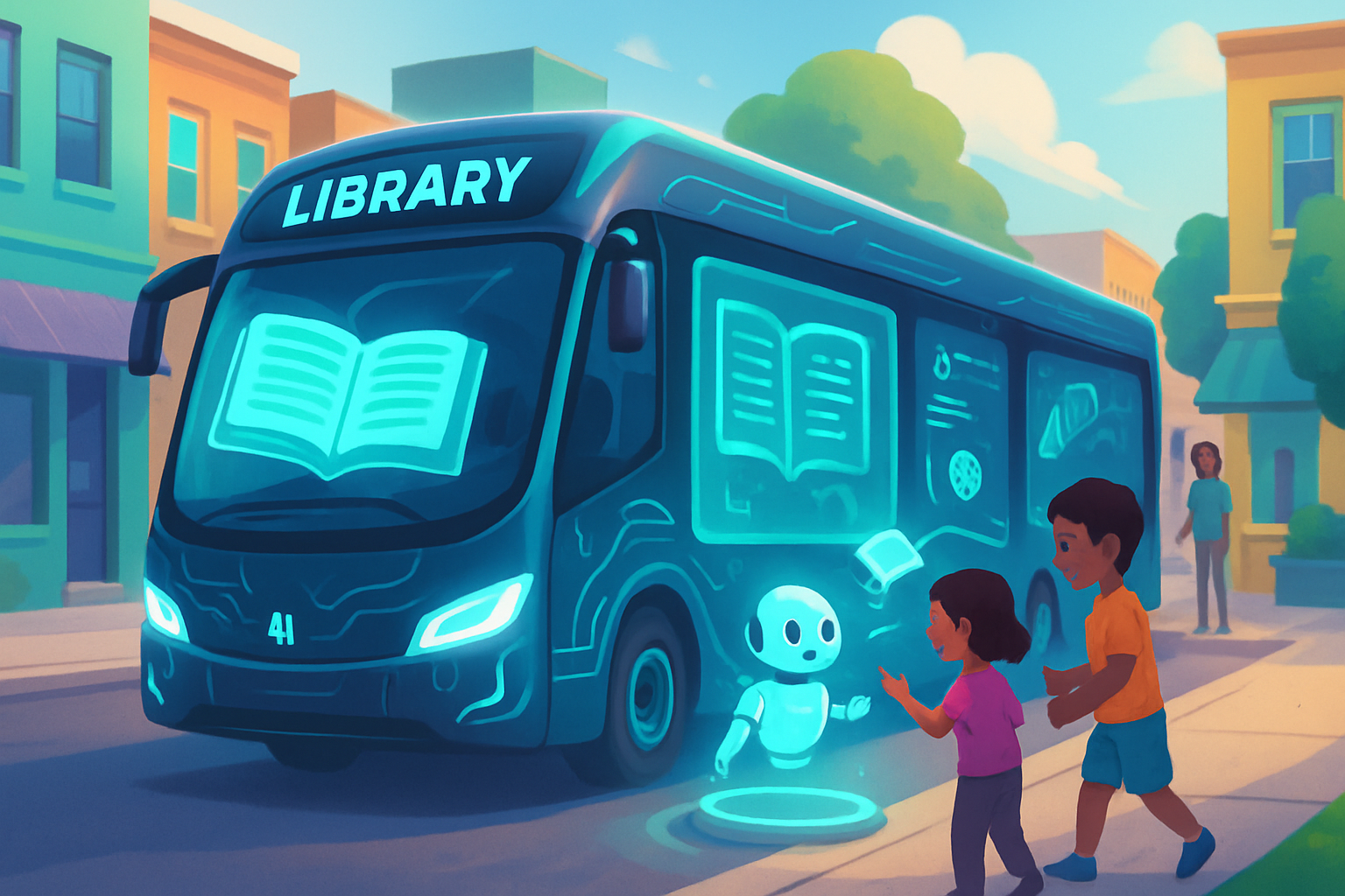
Tag: AI News

  • OpenAI Unleashes Dual Revolution: Near-Human AI Productivity and Immersive Video Creation with Sora

    OpenAI Unleashes Dual Revolution: Near-Human AI Productivity and Immersive Video Creation with Sora

    OpenAI (Private) has once again captured the global spotlight with two monumental announcements that collectively signal a new epoch in artificial intelligence. The company has unveiled a groundbreaking AI productivity benchmark demonstrating near-human performance across a vast array of professional tasks, simultaneously launching its highly anticipated standalone video application, Sora. These developments, arriving as of October 1, 2025, are poised to redefine the landscape of work, creativity, and digital interaction, fundamentally altering how industries operate and how individuals engage with AI-generated content.

    The immediate significance of these advancements is profound. The productivity benchmark, dubbed GDPval, provides tangible evidence of AI's burgeoning capacity to contribute economically at expert levels, challenging existing notions of human-AI collaboration. Concurrently, the public release of Sora, a sophisticated text-to-video generation platform now accessible as a dedicated app, ushers in an era where high-quality, long-form AI-generated video is not just a possibility but a readily available creative tool, complete with social features designed to foster a new ecosystem of digital content.

    Technical Milestones: Unpacking GDPval and Sora 2's Capabilities

    OpenAI's new GDPval (Gross Domestic Product Value) framework represents a significant leap from traditional academic evaluations, focusing instead on AI's practical, economic contributions. This benchmark meticulously assesses AI proficiency across over 1,300 specialized, economically valuable tasks spanning 44 professional occupations within nine major U.S. industries, including healthcare, finance, and legal services. Tasks range from drafting legal briefs and creating engineering blueprints to performing detailed financial analyses. The evaluation employs experienced human professionals to blindly compare AI-generated work against human expert outputs, judging whether the AI output is "better than," "as good as," or "worse than" human work.

    The findings are striking: frontier AI models are achieving or exceeding human-level proficiency in a significant percentage of these complex business tasks. Anthropic's (Private) Claude Opus 4.1 demonstrated exceptional performance, matching or exceeding expert quality in an impressive 47.6% of evaluated tasks, particularly excelling in aesthetic elements like document formatting. OpenAI's (Private) own GPT-5, released in Summer 2025, achieved expert-level performance in 40.6% of tasks, showcasing particular strength in accuracy-focused, domain-specific knowledge. This marks a dramatic improvement from its predecessor, GPT-4o (released Spring 2024), which scored only 13.7%, indicating that performance on GDPval tasks "more than doubled from GPT-4o to GPT-5." Beyond quality, OpenAI also reported staggering efficiency gains, stating that frontier models can complete GDPval tasks approximately 100 times faster and at 100 times lower costs compared to human experts, though these figures primarily reflect model inference time and API billing rates.

    Concurrently, the launch of OpenAI's (Private) standalone Sora app on October 1, 2025, introduces Sora 2, an advanced text-to-video generation model. Initially available for Apple iOS devices in the U.S. and Canada via an invite-only system, the app features a personalized, vertical, swipe-based feed akin to popular social media platforms but dedicated exclusively to AI-generated video content. Sora 2 brings substantial advancements: enhanced realism and physics accuracy, adeptly handling complex movements and interactions without common distortions; native integration of synchronized dialogue, sound effects, and background music; support for diverse styles and multi-shot consistency; and a groundbreaking "Cameo" feature. This "Cameo" allows users, after a one-time identity verification, to insert their own likeness and voice into AI-generated videos with high fidelity, maintaining control over their digital avatars. Unlike other AI video tools that primarily focus on generation, Sora is designed as a social app for creating, remixing, sharing, and discovering AI-generated videos, directly challenging consumer-facing platforms like TikTok (ByteDance (Private)), YouTube Shorts (Google (NASDAQ: GOOGL)), and Instagram Reels (Meta (NASDAQ: META)).

    Reshaping the AI Industry: Competitive Shifts and Market Disruption

    These dual announcements by OpenAI (Private) are set to profoundly impact AI companies, tech giants, and startups alike. Companies possessing or developing frontier models, such as OpenAI (Private), Anthropic (Private), Google (NASDAQ: GOOGL) with its Gemini 2.5 Pro, and xAI (Private) with Grok 4, stand to benefit immensely. The GDPval benchmark provides a new, economically relevant metric for validating their AI's capabilities, potentially accelerating enterprise adoption and investment in their technologies. Startups focused on AI-powered workflow orchestration and specialized professional tools will find fertile ground for integration, leveraging these increasingly capable models to deliver unprecedented value.

    The competitive landscape is intensifying. The rapid performance improvements highlighted by GDPval underscore the accelerated race towards Artificial General Intelligence (AGI), putting immense pressure on all major AI labs to innovate faster. The benchmark also shifts the focus from purely academic metrics to practical, real-world application, compelling companies to demonstrate tangible economic impact. OpenAI's (Private) foray into consumer social media with Sora directly challenges established tech giants like Meta (NASDAQ: META) and Google (NASDAQ: GOOGL), who have their own AI video initiatives (e.g., Google's (NASDAQ: GOOGL) Veo 3). By creating a dedicated platform for AI-generated video, OpenAI (Private) is not just providing a tool but building an ecosystem, potentially disrupting traditional content creation pipelines and the very nature of social media consumption.

    This dual strategy solidifies OpenAI's (Private) market positioning, cementing its leadership in both sophisticated enterprise AI solutions and cutting-edge consumer-facing applications. The potential for disruption extends to professional services, where AI's near-human performance could automate or augment significant portions of knowledge work, and to the creative industries, where Sora could democratize high-quality video production, challenging traditional media houses and content creators. Financial markets are already buzzing, anticipating potential shifts in market capitalization among technology giants as these developments unfold.

    Wider Significance: A New Era of Human-AI Interaction

    OpenAI's (Private) latest breakthroughs are not isolated events but pivotal moments within the broader AI landscape, signaling an undeniable acceleration towards advanced AI capabilities and their pervasive integration into society. The GDPval benchmark, by quantifying AI's economic value in professional tasks, blurs the lines between human and artificial output, suggesting a future where AI is not merely a tool but a highly capable co-worker. This fits into the overarching trend of AI moving from narrow, specialized tasks to broad, general-purpose intelligence, pushing the boundaries of what was once considered exclusively human domain.

    The impacts are far-reaching. Economically, we could see significant restructuring of industries, with productivity gains driving new forms of wealth creation but also raising critical questions about workforce transformation and job displacement. Socially, Sora's ability to generate highly realistic and customizable video content, especially with the "Cameo" feature, could revolutionize personal expression, storytelling, and digital identity. However, this also brings potential concerns: the proliferation of "AI slop" (low-effort, AI-generated content), the ethical implications of deepfakes, and the challenge of maintaining information integrity in an era where distinguishing between human and AI-generated content becomes increasingly difficult. OpenAI (Private) has implemented safeguards like C2PA metadata and watermarks, but the scale of potential misuse remains a significant societal challenge.

    These developments invite comparisons to previous technological milestones, such as the advent of the internet or the mobile revolution. Just as those technologies fundamentally reshaped communication and commerce, OpenAI's (Private) advancements could usher in a similar paradigm shift, redefining human creativity, labor, and interaction with digital realities. The rapid improvement from GPT-4o to GPT-5, as evidenced by GDPval, serves as a potent reminder of AI's exponential progress, fueling both excitement for future possibilities and apprehension about the pace of change.

    The Road Ahead: Anticipated Developments and Lingering Challenges

    Looking ahead, the near-term future promises rapid evolution stemming from these announcements. We can expect broader access to the Sora app beyond its initial invite-only, iOS-exclusive launch, with an Android version and international rollout likely on the horizon. Further iterations of the GDPval benchmark will likely emerge, incorporating more complex, interactive tasks and potentially leading to even higher performance scores as models continue to improve. Integration of these advanced AI capabilities into a wider array of professional tools and platforms, including those offered by TokenRing AI for multi-agent AI workflow orchestration, is also highly anticipated, streamlining operations across industries.

    In the long term, experts predict a future where AI becomes an increasingly ubiquitous co-worker, capable of fully autonomous agentic behavior in certain domains. The trajectory points towards the realization of AGI, where AI systems can perform any intellectual task a human can. Potential applications are vast, from highly personalized education and healthcare to entirely new forms of entertainment and scientific discovery. The "Cameo" feature in Sora, for instance, could evolve into sophisticated personal AI assistants that can represent users in virtual spaces.

    However, significant challenges remain. Ethical governance of powerful AI, ensuring fairness, transparency, and accountability, will be paramount. Issues of explainability (understanding how AI arrives at its conclusions) and robustness (AI's ability to perform reliably in varied, unforeseen circumstances) still need substantial research and development. Societal adaptation to widespread AI integration, including the need for continuous workforce reskilling and potential discussions around universal basic income, will be critical. What experts predict next is a continued, relentless pace of AI innovation, making it imperative for individuals, businesses, and governments to proactively engage with these technologies and shape their responsible deployment.

    A Pivotal Moment in AI History

    OpenAI's (Private) recent announcements—the GDPval benchmark showcasing near-human AI productivity and the launch of the Sora video app—mark a pivotal moment in the history of artificial intelligence. These dual advancements highlight AI's rapid maturation, moving beyond impressive demonstrations to deliver tangible economic value and unprecedented creative capabilities. The key takeaway is clear: AI is no longer a futuristic concept but a present-day force reshaping professional work and digital content creation.

    This development's significance in AI history cannot be overstated. It redefines the parameters of human-AI collaboration, setting new industry standards for performance evaluation and creative output. The ability of AI to perform complex professional tasks at near-human levels, coupled with its capacity to generate high-fidelity, long-form video, fundamentally alters our understanding of what machines are capable of. It pushes the boundaries of automation and creative expression, opening up vast new possibilities while simultaneously presenting profound societal and ethical questions.

    In the coming weeks and months, the world will be watching closely. Further iterations of the GDPval benchmark, the expansion and user adoption of the Sora app, and the regulatory responses to these powerful new capabilities will all be critical indicators of AI's evolving role. The long-term impact of these breakthroughs is likely to be transformative, affecting every facet of human endeavor and necessitating a thoughtful, adaptive approach to integrating AI into our lives.


    This content is intended for informational purposes only and represents analysis of current AI developments.

    TokenRing AI delivers enterprise-grade solutions for multi-agent AI workflow orchestration, AI-powered development tools, and seamless remote collaboration platforms. For more information, visit https://www.tokenring.ai/.

  • Silicon’s Green Revolution: How Advanced Chips are Powering the Renewable Energy Transition

    Silicon’s Green Revolution: How Advanced Chips are Powering the Renewable Energy Transition

    The global push towards a sustainable future is accelerating, and at its core lies an often-unsung hero: the semiconductor industry. Far from being merely the engine of our digital lives, advancements in chip technology are now proving indispensable in the renewable energy transition, driving unprecedented progress in how we generate, store, and manage sustainable power. This silent revolution, particularly propelled by emerging materials like organic semiconductors, is fundamentally reshaping the landscape of green energy solutions, promising a future where clean power is not only efficient but also ubiquitous and affordable.

    This pivotal role of semiconductors extends across the entire renewable energy ecosystem, from maximizing the efficiency of solar panels and wind turbines to enabling sophisticated battery management systems and intelligent smart grids. The immediate significance of these developments cannot be overstated; they are directly accelerating the adoption of renewable energy, enhancing grid resilience, and dramatically reducing the cost and accessibility barriers that have historically hindered widespread green energy deployment. As the world grapples with climate change and escalating energy demands, the continuous innovation within chip technology stands as a critical enabler for a truly sustainable future.

    Organic Semiconductors: A Technical Leap Towards Ubiquitous Green Energy

    The technical landscape of renewable energy is being profoundly reshaped by advancements in semiconductor technology, with organic semiconductors emerging as a particularly exciting frontier. Unlike traditional silicon-based chips, organic semiconductors are carbon-based molecules or polymers that offer a unique blend of properties, setting them apart as a game-changer for sustainable solutions.

    A significant breakthrough in organic solar cells (OSCs) has been the development of Non-Fullerene Acceptors (NFAs). These novel materials have dramatically boosted power conversion efficiencies, with laboratory results now approaching and even exceeding 19% in some instances. This is a crucial leap, as earlier organic solar cells often struggled with lower efficiencies, typically around 11%. NFAs address the challenge of exciton binding – where electron-hole pairs formed after light absorption are tightly bound – by facilitating more efficient charge separation. Furthermore, extensive molecular engineering allows researchers to precisely tune the band gap and other electronic properties of these materials, optimizing light absorption and charge transport. This design flexibility extends to creating new organic molecules, such as P3TTM, that exhibit quantum mechanical behaviors previously seen only in inorganic materials, potentially simplifying solar panel construction. Advanced device architectures, including bulk heterojunctions (BHJs) and multi-junction cells, are also being employed to maximize light capture across the solar spectrum and overcome the inherent short exciton diffusion lengths in organic materials.

    These technical specifications highlight the distinct advantages of organic semiconductors. Their inherent flexibility and lightweight nature mean they can be deposited onto flexible substrates using low-cost, low-temperature, solution-based processing methods like roll-to-roll printing. This contrasts sharply with the energy-intensive, high-temperature processes required for crystalline silicon. While commercial crystalline silicon cells typically boast efficiencies between 20% and 25%, the rapid improvement in organic solar cells, coupled with their semi-transparency and tunable properties, opens doors for novel applications like solar windows and integration into curved surfaces, which are impossible with rigid silicon. However, challenges remain, particularly regarding their shorter lifespan and lower charge carrier mobility compared to silicon, areas where active research is focused on improving stability under real-world conditions.

    The initial reactions from the AI research community and industry experts are a mix of optimism and pragmatism. There's widespread recognition of organic semiconductors as a "next-generation technology for a greener future" due to their sustainability, low fabrication cost, and diverse performance capabilities. Crucially, the AI community is actively contributing to this field, leveraging machine learning to accelerate the discovery of new materials, significantly reducing the experimental cycles needed for breakthroughs. Experts emphasize that while efficiency is important, the primary focus is now shifting towards enhancing long-term stability, scalability, and practical integration. The potential for low-cost, mass-produced plastic solar cells with a low embedded energy footprint is seen as a major market disruptor, although widespread commercial use in large-scale solar panels is still in its developmental stages, with existing applications primarily in consumer electronics displays.

    Corporate Fortunes and Competitive Shifts in the Green Chip Era

    The advent of advanced semiconductor technologies, particularly organic semiconductors, is poised to trigger significant shifts in corporate fortunes and reshape competitive landscapes across the tech and energy sectors. This revolution presents immense opportunities for agile innovators while demanding strategic recalibration from established giants.

    Companies specializing in Organic Photovoltaics (OPVs) and their material components are at the forefront of this benefit. Innovators like Heliatek GmbH, a pioneer in flexible organic solar films, are carving out niches in building-integrated photovoltaics (BIPV), automotive applications, and consumer electronics. Similarly, BELECTRIC OPV GmbH and ASCA are leveraging printed photovoltaic technology for customizable modules in smart textiles and architectural designs. Material specialists such as Novaled and Epishine are crucial, providing the high-performance organic materials and focusing on scalability for various appliances. Even traditional solar panel manufacturers like JinkoSolar (NYSE: JKS) and Vikram Solar could strategically integrate these technologies to diversify their offerings and tap into new markets. Beyond solar, the enhanced power management capabilities enabled by efficient organic semiconductors could indirectly benefit wind power giants like Vestas (CPH: VWS) and major Electric Vehicle (EV) manufacturers by optimizing energy flow and battery life.

    The competitive implications for major chip manufacturers and tech giants are profound. While organic semiconductors challenge the long-standing dominance of silicon due to their flexibility, lightweight nature, and lower production costs, they also present immense opportunities for tech titans. Companies like Apple (NASDAQ: AAPL), Google (NASDAQ: GOOGL), Samsung (KRX: 005930), and Amazon (NASDAQ: AMZN) stand to benefit significantly from integrating thin, flexible, and even transparent organic solar cells into consumer electronics, enabling self-charging capabilities and extended battery life for devices ranging from smartphones to VR headsets. This could lead to sleeker designs, enhanced product differentiation, and potentially transparent solar-harvesting displays. However, traditional semiconductor manufacturers must adapt. The shift towards more environmentally friendly, solution-based manufacturing processes for organic semiconductors could reduce reliance on the complex and often vulnerable global silicon supply chain. Major players may need to invest heavily in R&D, forge strategic partnerships, or acquire startups specializing in organic materials to secure intellectual property and manufacturing capabilities in this evolving domain. Material science giants like Merck KGaA (ETR: MRK), BASF SE (ETR: BAS), and Sumitomo Chemical (TYO: 4005) are already focusing on material diversification to capitalize on this trend.

    The disruptive potential of organic semiconductors is already evident in display technology, where Organic Light-Emitting Diodes (OLEDs) have largely supplanted Liquid Crystal Displays (LCDs) in small to medium-sized applications and dominate the premium television market. Companies like Samsung Display Co., Ltd. and LG Display Co., Ltd. (KRX: 034220) have been key disruptors here. Looking ahead, flexible, transparent, and ultra-light OPV films could disrupt traditional rooftop solar installations by enabling energy harvesting from unconventional surfaces like windows or curtains, creating entirely new markets. For low-power Internet of Things (IoT) devices, integrated organic solar cells could eliminate the need for conventional batteries, simplifying deployment and maintenance. Furthermore, Organic Thin-Film Transistors (OTFTs) are paving the way for mechanically flexible and foldable electronic products, leading to innovations like electronic paper and "smart" clothing. Companies that strategically invest in these areas will gain significant advantages in product differentiation, sustainability branding, and cost-effectiveness, potentially creating new market segments and securing robust intellectual property.

    A Broader Horizon: Integrating AI and Sustainability with Organic Chips

    The rise of organic semiconductors extends far beyond incremental improvements in renewable energy; it signifies a profound shift in the broader AI landscape and global sustainability efforts. This technology is not merely an alternative but a crucial enabler for a future where AI is more pervasive, efficient, and environmentally responsible.

    In the AI landscape, organic semiconductors are poised to facilitate a new generation of hardware. Their inherent flexibility and low-power characteristics make them ideal for the burgeoning fields of wearable AI, smart textiles, and implantable medical devices. Imagine biosensors seamlessly integrated into clothing for continuous health monitoring or flexible displays that adapt to any surface. Crucially, organic semiconductors are vital for low-power and edge AI applications, where processing occurs closer to the data source rather than in distant data centers. This reduces latency and energy consumption, critical for the proliferation of IoT devices. Furthermore, organic electronics hold immense potential for neuromorphic computing, which aims to mimic the human brain's structure and function. By enabling components that integrate sensing, memory, and processing—often separate in traditional systems—organic semiconductors can lead to significantly more energy-efficient and high-performing AI hardware. Paradoxically, AI itself is playing a pivotal role in accelerating this development, with machine learning algorithms rapidly discovering and optimizing new organic materials, significantly shortening the traditional trial-and-error approach in materials science.

    The societal and environmental impacts are equally transformative. Socially, biocompatible and flexible organic semiconductors promise to revolutionize healthcare with advanced monitoring and diagnostics, including innovative treatments like photovoltaic retinal prostheses. Their printability and lower production costs could also lead to more affordable and accessible electronics, helping to bridge technological divides globally. Environmentally, organic semiconductors offer a significant reduction in carbon footprint. Unlike conventional silicon, which demands energy-intensive, high-temperature manufacturing and often involves toxic metals, organic materials can be produced using low-temperature, less energy-intensive processes. Many are also biocompatible and biodegradable, offering a potential solution to the escalating problem of electronic waste (e-waste) by being recyclable like plastics. Organic photovoltaics (OPVs) provide a greener alternative to traditional silicon solar cells, utilizing earth-abundant materials and enabling seamless integration into buildings and vehicles through their transparent and flexible properties, expanding solar energy harvesting possibilities.

    However, potential concerns remain. While efficiency has improved dramatically, organic solar cells still generally have shorter lifespans and lower power conversion efficiencies compared to crystalline silicon, with degradation due to environmental factors being a persistent challenge. Scalability of manufacturing for high-performance organic devices also needs further optimization. Moreover, the energy consumption of the AI tools used to discover these materials presents an interesting paradox, underscoring the need for energy-efficient AI practices. Geopolitical factors, resource constraints, and trade restrictions impacting the broader semiconductor industry could also affect the supply chain and adoption of organic semiconductors. When compared to previous AI and energy milestones, organic semiconductors represent a fundamental paradigm shift. In AI, they move beyond the limitations of rigid, energy-intensive silicon, enabling a future of pervasive, low-power, and flexible intelligence. In energy, they herald a "greener" third wave of solar technology, moving beyond the rigidity and e-waste concerns of traditional silicon panels towards a future where energy harvesting is seamlessly integrated into our built environment, akin to how the invention of the electric generator revolutionized energy distribution. This evolution signifies a concerted move towards sustainable technological progress.

    The Road Ahead: Unlocking the Full Potential of Organic Chips for Green Energy

    The trajectory of organic semiconductors in renewable energy is one of continuous innovation and expanding horizons. Both near-term and long-term developments promise to solidify their role as a cornerstone of sustainable power, although significant challenges must still be navigated for widespread commercial viability.

    In the near term (the next 1-5 years), we can expect to see organic photovoltaic (OPV) cells push laboratory power conversion efficiencies (PCEs) beyond the 20% mark for single-junction cells, building on the success of non-fullerene acceptors (NFAs). This will bring them increasingly closer to the performance of traditional silicon. A critical focus will also be on significantly improving long-term operational stability and durability under diverse environmental conditions, with ongoing research in phase stabilization and compositional engineering. Furthermore, the industry will concentrate on scaling up manufacturing processes from laboratory to commercial-scale production, leveraging solution-based methods like roll-to-roll printing to reduce costs and complexity. A deeper understanding of fundamental electronic processes, such as "entropy-driven charge separation" in NFAs, will continue to drive these improvements.

    Looking further ahead, the long-term vision includes the development of highly efficient hybrid organic-perovskite tandem cells, designed to capture an even broader spectrum of light. Advanced material design, process refinement, and interface engineering will further augment the efficiency and durability of OPVs. Crucially, Artificial Intelligence (AI), particularly machine learning, is predicted to play a paramount role in accelerating the discovery and optimization of new organic solar materials and device designs, analyzing vast datasets to predict PCE and stability with unprecedented speed. This synergistic relationship between AI and material science will be key to unlocking the full potential of organic semiconductors. The widespread adoption of transparent and flexible organic solar cells for building-integrated photovoltaics (BIPV), smart windows, and self-powered smart textiles is also on the horizon, enabling a truly distributed energy generation model. Beyond solar, organic thermoelectrics (OTEs) are being developed to convert waste heat into electricity, offering flexible and environmentally friendly solutions for waste heat recovery in various applications.

    These unique properties—flexibility, lightweight nature, transparency, and low-cost manufacturing—open up a vast array of potential applications. Transparent organic solar cells can be seamlessly integrated into windows and facades, transforming buildings into active energy generators. Flexible organic films can power wearable devices and smart textiles, providing portable energy for consumer electronics. EVs could incorporate organic solar cells into sunroofs or body panels to extend range. Their adaptability makes them ideal for off-grid and remote power solutions, while semi-transparent versions could enable "agrivoltaics" in greenhouses, generating electricity while supporting plant growth. Experts predict that organic solar cells will carve out a distinct market niche rather than directly replacing silicon for large utility-scale installations. Their value will lie in their adaptability, aesthetic appeal, and lower installation and transportation costs. The future promises continued rapid evolution, driven by ongoing research and the accelerating influence of AI, leading to a broader range of applications and a strong focus on sustainability. However, challenges in narrowing the efficiency gap with silicon, ensuring long-term stability and durability, and achieving cost-effective large-scale manufacturing remain critical hurdles that must be addressed for organic semiconductors to achieve widespread commercial viability.

    A Sustainable Future Powered by Advanced Semiconductors

    The semiconductor industry's pivotal role in the renewable energy transition, particularly through the advancements in organic semiconductor technology, is a narrative of profound significance for both AI and global sustainability. Key takeaways highlight that semiconductors are not just components but the foundational infrastructure enabling efficient green energy generation, storage, and management. Organic semiconductors, with their inherent flexibility, lightweight properties, and potential for low-cost, environmentally friendly manufacturing, are emerging as a transformative force, promising to democratize access to clean energy and reduce the ecological footprint of electronics.

    This development marks a crucial juncture in both AI history and the energy transition. For AI, it paves the way for a new generation of low-power, flexible, and pervasive intelligent systems, from wearable AI to neuromorphic computing, moving beyond the limitations of rigid silicon. For energy, it represents a "greener" third wave of solar technology, offering versatile and integrated energy harvesting solutions that can seamlessly blend into our built environment. The long-term impact is a fundamental shift towards a future where technology is inherently more sustainable, with high-performance computing coexisting harmoniously with environmental responsibility.

    In the coming weeks and months, watch for continued breakthroughs in the efficiency and stability of organic photovoltaics, particularly as they scale to larger modules. Keep an eye on new material science discoveries, especially in non-fullerene acceptors, and advancements in solution-based processing and printing techniques that will enable low-cost, large-scale manufacturing. The synergistic role of AI in accelerating the design and discovery of these new materials will be a powerful indicator of progress. Finally, observe the expansion of organic semiconductor applications beyond traditional displays into flexible electronics, smart packaging, IoT devices, transparent solar cells for building integration, and hybrid technologies combining organic layers with inorganic semiconductors to achieve even higher efficiencies. The organic semiconductor market is projected for substantial expansion, signaling a future where these innovative chips are integral to both renewable energy solutions and next-generation AI hardware.

    This content is intended for informational purposes only and represents analysis of current AI developments.

    TokenRing AI delivers enterprise-grade solutions for multi-agent AI workflow orchestration, AI-powered development tools, and seamless remote collaboration platforms.
    For more information, visit https://www.tokenring.ai/.

  • The Atomic Edge: How Novel Materials Are Forging the Future of AI Chips

    The Atomic Edge: How Novel Materials Are Forging the Future of AI Chips

    The relentless pursuit of computational power, fueled by the explosive growth of artificial intelligence, is pushing the semiconductor industry to its fundamental limits. As traditional silicon-based technologies approach their physical boundaries, a new frontier is emerging: advanced materials science. This critical field is not merely enhancing existing chip designs but is fundamentally redefining what's possible, ushering in an era where novel materials are the key to unlocking unprecedented chip performance, functionality, and energy efficiency. From wide-bandgap semiconductors powering electric vehicles to atomically thin 2D materials promising ultra-fast transistors, the microscopic world of atoms and electrons is now dictating the macroscopic capabilities of our digital future.

    This revolution in materials is poised to accelerate the development of next-generation AI, high-performance computing, and edge devices. By offering superior electrical, thermal, and mechanical properties, these advanced compounds are enabling breakthroughs in processing speed, power management, and miniaturization, directly addressing the insatiable demands of increasingly complex AI models and data-intensive applications. The immediate significance lies in overcoming the bottlenecks that silicon alone can no longer resolve, paving the way for innovations that were once considered theoretical, and setting the stage for a new wave of technological progress across diverse industries.

    Beyond Silicon: A Deep Dive into the Materials Revolution

    The core of this materials revolution lies in moving beyond the inherent limitations of silicon. While silicon has been the bedrock of the digital age, its electron mobility and thermal conductivity are finite, especially as transistors shrink to atomic scales. Novel materials offer pathways to transcend these limits, enabling faster switching speeds, higher power densities, and significantly reduced energy consumption.

    Wide-Bandgap (WBG) Semiconductors are at the forefront of this shift, particularly Gallium Nitride (GaN) and Silicon Carbide (SiC). Unlike silicon, which has a bandgap of 1.1 electron volts (eV), GaN boasts 3.4 eV and SiC 3.3 eV. This wider bandgap translates directly into several critical advantages. Devices made from GaN and SiC can operate at much higher voltages, temperatures, and frequencies without breaking down. This allows for significantly faster switching speeds, which is crucial for power electronics in applications like electric vehicle chargers, 5G infrastructure, and data center power supplies. Their superior thermal conductivity also means less heat generation and more efficient power conversion, directly impacting the energy footprint of AI hardware. For instance, a GaN-based power transistor can switch thousands of times faster than a silicon equivalent, dramatically reducing energy loss. Initial reactions from the power electronics community have been overwhelmingly positive, with widespread adoption in specific niches and a clear roadmap for broader integration.

    Two-Dimensional (2D) Materials represent an even more radical departure from traditional bulk semiconductors. Graphene, a single layer of carbon atoms arranged in a hexagonal lattice, exemplifies this category. Renowned for its extraordinary electron mobility (up to 100 times that of silicon) and thermal conductivity, graphene has long been hailed for its potential in ultra-fast transistors and interconnects. While its lack of an intrinsic bandgap posed challenges for digital logic, recent breakthroughs in engineering semiconducting graphene with useful bandgaps have revitalized its prospects. Other 2D materials, such as Molybdenum Disulfide (MoS2) and other Transition Metal Dichalcogenides (TMDs), also offer unique advantages. MoS2, for example, possesses a stable bandgap nearly twice that of silicon, making it a promising candidate for flexible electronics and next-generation transistors. These materials' atomic-scale thickness is paramount for continued miniaturization, pushing the boundaries of Moore's Law and enabling novel device architectures that can be stacked in 3D configurations without significant performance degradation. The AI research community is particularly interested in 2D materials for neuromorphic computing and edge AI, where ultra-low power and high-density integration are critical.

    Beyond these, Carbon Nanotubes (CNTs) are gaining traction as a more mature 2D technology, offering tunable electrical properties and ultra-high carrier mobilities, with practical transistors already fabricated at sub-10nm scales. Hafnium Oxide is being manipulated to achieve stable ferroelectric properties, enabling co-location of computation and memory on a single chip, drastically reducing energy consumption for AI workloads. Furthermore, Indium-based materials are being developed to facilitate Extreme Ultraviolet (EUV) lithography, crucial for creating smaller, more precise features and enabling advanced 3D circuit production without damaging existing layers. These materials collectively represent a paradigm shift, moving chip design from merely shrinking existing structures to fundamentally reimagining the building blocks themselves.

    Corporate Giants and Nimble Startups: Navigating the New Material Frontier

    The shift towards advanced materials in semiconductor development is not just a technical evolution; it's a strategic battleground with profound implications for AI companies, tech giants, and ambitious startups alike. The race to integrate Gallium Nitride (GaN), Silicon Carbide (SiC), and 2D materials is reshaping competitive landscapes and driving significant investment.

    Leading the charge in GaN and SiC are established power semiconductor players. Companies like Wolfspeed (NYSE: WOLF), formerly Cree, Inc., are dominant in SiC wafers and devices, crucial for electric vehicles and renewable energy. STMicroelectronics N.V. (NYSE: STM) is heavily invested in SiC, expanding production facilities to meet surging automotive demand. Infineon Technologies AG (ETR: IFX) and ON Semiconductor (NASDAQ: ON) are also major players, making significant advancements in both GaN and SiC for power conversion and automotive applications. In the GaN space, specialized firms such as Navitas Semiconductor (NASDAQ: NVTS) and Efficient Power Conversion Corporation (EPC) are challenging incumbents with innovative GaN power ICs, enabling smaller, faster chargers and more efficient power supplies for consumer electronics and data centers. These companies stand to benefit immensely from the growing demand for high-efficiency power solutions, directly impacting the energy footprint of AI infrastructure.

    For major AI labs and tech giants like Google (NASDAQ: GOOGL), Samsung Electronics (KRX: 005930), TSMC (NYSE: TSM), and Intel Corporation (NASDAQ: INTC), the competitive implications are immense. These companies are not just consumers of advanced chips but are also heavily investing in research and development of these materials to enhance their custom AI accelerators (like Google's TPUs) and next-generation processors. The ability to integrate these materials will directly translate to more powerful, energy-efficient AI hardware, providing a significant competitive edge in training massive models and deploying AI at scale. For instance, better power efficiency means lower operating costs for vast data centers running AI workloads, while faster chips enable quicker iterations in AI model development. The race for talent in materials science and semiconductor engineering is intensifying, becoming a critical factor in maintaining leadership.

    This materials revolution also presents a fertile ground for startups. Niche players specializing in custom chip design for AI, IoT, and edge computing, or those developing novel fabrication techniques for 2D materials, can carve out significant market shares. Companies like Graphenea and 2D Materials Pte Ltd are focusing on the commercialization of graphene and other 2D materials, creating foundational components for future devices. However, startups face substantial hurdles, including the capital-intensive nature of semiconductor R&D and manufacturing, which can exceed $15 billion for a cutting-edge fabrication plant. Nevertheless, government initiatives, such as the CHIPS Act, aim to foster innovation and support both established and emerging players in these critical areas. The disruption to existing products is already evident: GaN-based fast chargers are rapidly replacing traditional silicon chargers, and SiC is becoming standard in high-performance electric vehicles, fundamentally altering the market for power electronics and automotive components.

    A New Era of Intelligence: Broader Implications and Future Trajectories

    The fusion of advanced materials science with semiconductor development is not merely an incremental upgrade; it represents a foundational shift that profoundly impacts the broader AI landscape and global technological trends. This revolution is enabling new paradigms of computing, pushing the boundaries of what AI can achieve, and setting the stage for unprecedented innovation.

    At its core, this materials-driven advancement is enabling AI-specific hardware to an extent never before possible. The insatiable demand for processing power for tasks like large language model training and generative AI inference has led to the creation of specialized chips such as Tensor Processing Units (TPUs) and Application-Specific Integrated Circuits (ASICs). Advanced materials allow for greater transistor density, reduced latency, and significantly lower power consumption in these accelerators, directly fueling the rapid progress in AI capabilities. Furthermore, the development of neuromorphic computing, inspired by the human brain, relies heavily on novel materials like phase-change materials and memristive oxides (e.g., hafnium oxide). These materials are crucial for creating devices that mimic synaptic plasticity, allowing for in-memory computation and vastly more energy-efficient AI systems that overcome the limitations of traditional Von Neumann architectures. This shift from general-purpose computing to highly specialized, biologically inspired hardware represents a profound architectural change, akin to the shift from early vacuum tube computers to integrated circuits.

    The wider impacts of this materials revolution are vast. Economically, it fuels a "trillion-dollar sector" of AI and semiconductors, driving innovation, creating new job opportunities, and fostering intense global competition. Technologically, more powerful and energy-efficient semiconductors are accelerating advancements across nearly every sector, from autonomous vehicles and IoT devices to healthcare and industrial automation. AI itself is becoming a critical tool in this process, with AI for AI becoming a defining trend. AI algorithms are now used to predict material properties, optimize chip architectures, and even automate parts of the manufacturing process, significantly reducing R&D time and costs. This symbiotic relationship, where AI accelerates the discovery of the very materials that power its future, was not as prominent in earlier AI milestones and marks a new era of self-referential advancement.

    However, this transformative period is not without its potential concerns. The immense computational power required by modern AI models, even with more efficient hardware, still translates to significant energy consumption, posing environmental and economic challenges. The technical hurdles in designing and manufacturing with these novel materials are enormous, requiring billions of dollars in R&D and sophisticated infrastructure, which can create barriers to entry. There's also a growing skill gap, as the industry demands a workforce proficient in both advanced materials science and AI/data science. Moreover, the extreme concentration of advanced semiconductor design and production among a few key global players (e.g., NVIDIA Corporation (NASDAQ: NVDA), TSMC (NYSE: TSM)) raises geopolitical tensions and concerns about supply chain vulnerabilities. Compared to previous AI milestones, where progress was often driven by Moore's Law and software advancements, the current era is defined by a "more than Moore" approach, prioritizing energy efficiency and specialized hardware enabled by groundbreaking materials science.

    The Road Ahead: Future Developments and the Dawn of a New Computing Era

    The journey into advanced materials science for semiconductors is just beginning, promising a future where computing capabilities transcend current limitations. Both near-term and long-term developments are poised to reshape industries and unlock unprecedented technological advancements.

    In the near-term (1-5 years), the increased adoption and refinement of Gallium Nitride (GaN) and Silicon Carbide (SiC) will continue its aggressive trajectory. These wide-bandgap semiconductors will solidify their position as the materials of choice for power electronics, driving significant improvements in electric vehicles (EVs), 5G infrastructure, and data center efficiency. Expect to see faster EV charging, more compact and efficient power adapters, and robust RF components for next-generation wireless networks. Simultaneously, advanced packaging materials will become even more critical. As traditional transistor scaling slows, the industry is increasingly relying on 3D stacking and chiplet architectures to boost performance and reduce power consumption. New polymers and bonding materials will be essential for integrating these complex, multi-die systems, especially for high-performance computing and AI accelerators.

    Looking further into the long-term (5+ years), more exotic and transformative materials are expected to emerge from research labs into commercial viability. Two-Dimensional (2D) materials like graphene and Transition Metal Dichalcogenides (TMDs) such as Molybdenum Disulfide (MoS2) hold immense promise. Recent breakthroughs in creating semiconducting graphene with a viable bandgap on silicon carbide substrates (demonstrated in 2024) are a game-changer, paving the way for ultra-fast graphene transistors in digital applications. Other 2D materials offer direct bandgaps and high stability, crucial for flexible electronics, optoelectronics, and advanced sensors. Experts predict that while silicon will remain dominant for some time, these new electronic materials could begin displacing it in mass-market devices from the mid-2030s, each finding optimal application-specific use cases. Materials like diamond, with its ultrawide bandgap and superior thermal conductivity, are being researched for heavy-duty power electronics, particularly as renewable energy sources become more prevalent. Carbon Nanotubes (CNTs) are also maturing, with advancements in material quality enabling practical transistor fabrication.

    The potential applications and use cases on the horizon are vast. Beyond enhanced power electronics and high-speed communication, these materials will enable entirely new forms of computing. Ultra-fast computing systems leveraging graphene, next-generation AI accelerators, and even the fundamental building blocks for quantum computing will all benefit. Flexible and wearable electronics will become more sophisticated, with advanced sensors for health monitoring and devices that seamlessly adapt to their environment. However, significant challenges need to be addressed. Manufacturing and scalability remain paramount concerns, as integrating novel materials into existing, highly complex fabrication processes is a monumental task, requiring high-quality production and defect reduction. Cost constraints, particularly the high initial investments and production expenses, must be overcome to achieve parity with silicon. Furthermore, ensuring a robust and diversified supply chain for these often-scarce elements and addressing the growing talent shortage in materials science and semiconductor engineering are critical for sustained progress. Experts predict a future of application-specific material selection, where different materials are optimized for different tasks, leading to a highly diverse and specialized semiconductor ecosystem, all driven by the relentless demand from AI and enabled by strategic investments and collaborations across the globe.

    The Atomic Foundation of AI's Future: A Concluding Perspective

    The journey into advanced materials science in semiconductor development marks a pivotal moment in technological history, fundamentally redefining the trajectory of artificial intelligence and high-performance computing. As the physical limits of silicon-based technologies become increasingly apparent, the continuous pursuit of novel materials has emerged not just as an option, but as an absolute necessity to push the boundaries of chip performance and functionality.

    The key takeaways from this materials revolution are clear: it's a move beyond mere miniaturization to a fundamental reimagining of the building blocks of computing. Wide-bandgap semiconductors like GaN and SiC are already transforming power electronics, enabling unprecedented efficiency and reliability in critical applications like EVs and 5G. Simultaneously, atomically thin 2D materials like graphene and MoS2 promise ultra-fast, energy-efficient transistors and novel device architectures for future AI and flexible electronics. This shift is creating intense competition among tech giants, fostering innovation among startups, and driving significant strategic investments in R&D and manufacturing infrastructure.

    This development's significance in AI history cannot be overstated. It represents a "more than Moore" era, where performance gains are increasingly derived from materials innovation and advanced packaging rather than just transistor scaling. It’s enabling the rise of specialized AI hardware, neuromorphic computing, and even laying the groundwork for quantum technologies, all designed to meet the insatiable demands of increasingly complex AI models. The symbiotic relationship where AI itself accelerates the discovery and design of these new materials is a testament to the transformative power of this convergence.

    Looking ahead, the long-term impact will be a computing landscape characterized by unparalleled speed, energy efficiency, and functional diversity. While challenges in manufacturing scalability, cost, and supply chain resilience remain, the momentum is undeniable. What to watch for in the coming weeks and months are continued breakthroughs in 2D material integration, further commercialization of GaN and SiC across broader applications, and strategic partnerships and investments aimed at securing leadership in this critical materials frontier. The atomic edge is where the future of AI is being forged, promising a new era of intelligence built on a foundation of revolutionary materials.

    This content is intended for informational purposes only and represents analysis of current AI developments.

    TokenRing AI delivers enterprise-grade solutions for multi-agent AI workflow orchestration, AI-powered development tools, and seamless remote collaboration platforms.
    For more information, visit https://www.tokenring.ai/.

  • Taiwan Rejects US Semiconductor Split, Solidifying “Silicon Shield” Amidst Global Supply Chain Reshuffle

    Taiwan Rejects US Semiconductor Split, Solidifying “Silicon Shield” Amidst Global Supply Chain Reshuffle

    Taipei, Taiwan – October 1, 2025 – In a move that reverberates through global technology markets and geopolitical strategists, Taiwan has firmly rejected a United States proposal for a 50/50 split in semiconductor production. Vice Premier Cheng Li-chiun, speaking on October 1, 2025, unequivocally stated that such a condition was "not discussed" and that Taiwan "will not agree to such a condition." This decisive stance underscores Taiwan's unwavering commitment to maintaining its strategic control over the advanced chip industry, often referred to as its "silicon shield," and carries immediate, far-reaching implications for the resilience and future architecture of global semiconductor supply chains.

    The decision highlights a fundamental divergence in strategic priorities between the two allies. While the U.S. has been aggressively pushing for greater domestic semiconductor manufacturing capacity, driven by national security concerns and the looming threat of substantial tariffs on imported chips, Taiwan views its unparalleled dominance in advanced chip fabrication as a critical geopolitical asset. This rejection signals Taiwan's determination to leverage its indispensable role in the global tech ecosystem, even as it navigates complex trade negotiations and implements its own ambitious strategies for technological sovereignty. The global tech community is now closely watching how this development will reshape investment flows, strategic partnerships, and the very foundation of AI innovation worldwide.

    Taiwan's Strategic Gambit: Diversifying While Retaining the Crown Jewels

    Taiwan's semiconductor diversification strategy, as it stands in October 2025, represents a sophisticated balancing act: expanding its global manufacturing footprint to mitigate geopolitical risks and meet international demands, while resolutely safeguarding its most advanced technological prowess on home soil. This approach marks a significant departure from historical models, which primarily focused on consolidating cutting-edge production within Taiwan for maximum efficiency and cost-effectiveness.

    At the heart of this strategy is the geographic diversification led by industry titan Taiwan Semiconductor Manufacturing Company (TSMC) (NYSE: TSM). By 2025, TSMC aims to establish 10 new global facilities, with three significant ventures in the United States (Arizona, with a colossal $65 billion investment for three fabs, the first 4nm facility expected to start production in early 2025), two in Japan (Kumamoto, with the first plant already operational since February 2023), and a joint venture in Europe (European Semiconductor Manufacturing Company – ESMC in Dresden, Germany). Taiwanese chip manufacturers are also exploring opportunities in Southeast Asia to cater to Western markets seeking to de-risk their supply chains from China. Simultaneously, there's a gradual scaling back of presence in mainland China by Taiwanese chipmakers, underscoring a strategic pivot towards "non-red" supply chains.

    Crucially, while expanding its global reach, Taiwan is committed to retaining its most advanced research and development (R&D) and manufacturing capabilities—specifically 2nm and 1.6nm processes—within its borders. TSMC is projected to break ground on its 1.4-nanometer chip manufacturing facilities in Taiwan this very month, with mass production slated for the latter half of 2028. This commitment ensures that Taiwan's "silicon shield" remains robust, preserving its technological leadership in cutting-edge fabrication. Furthermore, the National Science and Technology Council (NSTC) launched the "IC Taiwan Grand Challenge" in 2025 to bolster Taiwan's position as an IC startup cluster, offering incentives and collaborating with leading semiconductor companies, with a strong focus on AI chips, AI algorithms, and high-speed transmission technologies.

    This current strategy diverges sharply from previous approaches that prioritized a singular, domestically concentrated, cost-optimized model. Historically, Taiwan's "developmental state model" fostered a highly efficient ecosystem, allowing companies like TSMC to perfect the "pure-play foundry" model. The current shift is primarily driven by geopolitical imperatives rather than purely economic ones, aiming to address cross-strait tensions and respond to international calls for localized production. While the industry acknowledges the strategic importance of these diversification efforts, initial reactions highlight the increased costs associated with overseas manufacturing. TSMC, for instance, anticipates 5-10% price increases for advanced nodes and a potential 50% surge for 2nm wafers. Despite these challenges, the overwhelming demand for AI-related technology is a significant driver, pushing chip manufacturers to strategically direct R&D and capital expenditure towards high-growth AI areas, confirming a broader industry shift from a purely cost-optimized model to one that prioritizes security and resilience.

    Ripple Effects: How Diversification Reshapes the AI Landscape and Tech Giants' Fortunes

    The ongoing diversification of the semiconductor supply chain, accelerated by Taiwan's strategic maneuvers, is sending profound ripple effects across the entire technology ecosystem, particularly impacting AI companies, tech giants, and nascent startups. As of October 2025, the industry is witnessing a complex interplay of opportunities, heightened competition, and strategic realignments driven by geopolitical imperatives, the pursuit of resilience, and the insatiable demand for AI chips.

    Leading foundries and integrated device manufacturers (IDMs) are at the forefront of this transformation. Taiwan Semiconductor Manufacturing Company (TSMC) (NYSE: TSM), despite its higher operational costs in new regions, stands to benefit from mitigating geopolitical risks and securing access to crucial markets through its global expansion. Its continued dominance in advanced nodes (3nm, 5nm, and upcoming 2nm and 1.6nm) and advanced packaging technologies like CoWoS makes it an indispensable partner for AI leaders such as NVIDIA (NASDAQ: NVDA) and Advanced Micro Devices (NASDAQ: AMD). Similarly, Samsung Electronics (KRX: 005930) is aggressively challenging TSMC with plans for 2nm production in 2025 and 1.4nm by 2027, bolstered by significant U.S. CHIPS Act funding for its Taylor, Texas plant. Intel (NASDAQ: INTC) is also making a concerted effort to reclaim process technology leadership through its Intel Foundry Services (IFS) strategy, with its 18A process node entering "risk production" in April 2025 and high-volume manufacturing expected later in the year. This intensified competition among foundries could lead to faster technological advancements and offer more choices for chip designers, albeit with the caveat of potentially higher costs.

    AI chip designers and tech giants are navigating this evolving landscape with a mix of strategic partnerships and in-house development. NVIDIA (NASDAQ: NVDA), identified by KeyBanc as an "unrivaled champion," continues to see demand for its Blackwell AI chips outstrip supply for 2025, necessitating expanded advanced packaging capacity. Advanced Micro Devices (NASDAQ: AMD) is aggressively positioning itself as a full-stack AI and data center rival, making strategic acquisitions and developing in-house AI models. Hyperscalers like Microsoft (NASDAQ: MSFT), Apple (NASDAQ: AAPL), and Meta Platforms (NASDAQ: META) are deeply reliant on advanced AI chips and are forging long-term contracts with leading foundries to secure access to cutting-edge technology. Micron Technology (NASDAQ: MU), a recipient of substantial CHIPS Act funding, is also strategically expanding its global manufacturing footprint to enhance supply chain resilience and capture demand in burgeoning markets.

    For startups, this era of diversification presents both challenges and unique opportunities. While the increased costs of localized production might be a hurdle, the focus on regional ecosystems and indigenous capabilities is fostering a new wave of innovation. Agile AI chip startups are attracting significant venture capital, developing specialized solutions like customizable RISC-V-based applications, chiplets, LLM inference chips, and photonic ICs. Emerging regions like Southeast Asia and India are gaining traction as alternative manufacturing hubs, offering cost advantages and government incentives, creating fertile ground for new players. The competitive implications are clear: the push for domestic production and regional partnerships is leading to a more fragmented global supply chain, potentially resulting in inefficiencies and higher production costs, but also fostering divergent AI ecosystems as countries prioritize technological self-reliance. The intensified "talent wars" for skilled semiconductor professionals further underscore the transformative nature of this supply chain reshuffle, where strategic alliances, IP development, and workforce development are becoming paramount.

    A New Global Order: Geopolitics, Resilience, and the AI Imperative

    The diversification of the semiconductor supply chain, underscored by Taiwan's firm stance against a mandated production split, is not merely an industrial adjustment; it represents a fundamental reordering of global technology and geopolitical power, with profound implications for the burgeoning field of Artificial Intelligence. As of October 2025, this strategic pivot is reshaping how critical technologies are designed, manufactured, and distributed, driven by an unprecedented confluence of national security concerns, lessons learned from past disruptions, and the insatiable demand for advanced AI capabilities.

    At its core, semiconductors are the bedrock of the AI revolution. From the massive data centers training large language models to the compact devices performing real-time inference at the edge, every facet of AI development and deployment hinges on access to advanced chips. The current drive for supply chain diversification fits squarely into this broader AI landscape by seeking to ensure a stable and secure flow of these essential components. It supports the exponential growth of AI hardware, accelerates innovation in specialized AI chip designs (such as NPUs, TPUs, and ASICs), and facilitates the expansion of Edge AI, which processes data locally on devices, addressing critical concerns around privacy, latency, and connectivity. Hardware, once considered a commodity, has re-emerged as a strategic differentiator, prompting governments and major tech companies to invest unprecedented sums in AI infrastructure.

    However, this strategic reorientation is not without its significant concerns and formidable challenges. The most immediate is the substantial increase in costs. Reshoring or "friend-shoring" semiconductor manufacturing to regions like the U.S. or Europe can be dramatically more expensive than production in East Asia, with estimates suggesting costs up to 55% higher in the U.S. These elevated capital expenditures for new fabrication plants (fabs) and duplicated efforts across regions will inevitably lead to higher production costs, potentially impacting the final price of AI-powered products and services. Furthermore, the intensifying U.S.-China semiconductor rivalry has ushered in an era of geopolitical complexities and market bifurcation. Export controls, tariffs, and retaliatory measures are forcing companies to align with specific geopolitical blocs, creating "friend-shoring" strategies that, while aiming for resilience, can still be vulnerable to rapidly changing trade policies and compliance burdens.

    Comparing this moment to previous tech milestones reveals a distinct difference: the unprecedented geopolitical centrality. Unlike the PC revolution or the internet boom, where supply chain decisions were largely driven by cost-efficiency, the current push is heavily influenced by national security imperatives. Governments worldwide are actively intervening with massive subsidies – like the U.S. CHIPS and Science Act, the European Chips Act, and India's Semicon India Programme – to achieve technological sovereignty and reduce reliance on single manufacturing hubs. This state-led intervention and the sheer scale of investment in new fabs and R&D signify a strategic industrial policy akin to an "infrastructure arms race," a departure from previous eras. The shift from a "just-in-time" to a "just-in-case" inventory philosophy, driven by lessons from the COVID-19 pandemic, further underscores this prioritization of resilience over immediate cost savings. This complex, costly, and geopolitically charged undertaking is fundamentally reshaping how critical technologies are designed, manufactured, and distributed, marking a new chapter in global technological evolution.

    The Road Ahead: Navigating a Fragmented, Resilient, and AI-Driven Semiconductor Future

    The global semiconductor industry, catalyzed by geopolitical tensions and the insatiable demand for Artificial Intelligence, is embarking on a transformative journey towards diversification and resilience. As of October 2025, the landscape is characterized by ambitious governmental initiatives, strategic corporate investments, and a fundamental re-evaluation of supply chain architecture. The path ahead promises a more geographically distributed, albeit potentially costlier, ecosystem, with profound implications for technological innovation and global power dynamics.

    In the near term (October 2025 – 2026), we can expect an acceleration of reshoring and regionalization efforts, particularly in the U.S., Europe, and India, driven by substantial public investments like the U.S. CHIPS Act and the European Chips Act. This will translate into continued, significant capital expenditure in new fabrication plants (fabs) globally, with projections showing the semiconductor market allocating $185 billion for manufacturing capacity expansion in 2025. Workforce development programs will also ramp up to address the severe talent shortages plaguing the industry. The relentless demand for AI chips will remain a primary growth driver, with AI chips forecasted to experience over 30% growth in 2025, pushing advancements in chip design and manufacturing, including high-bandwidth memory (HBM). While market normalization is anticipated in some segments, rolling periods of constraint environments for certain chip node sizes, exacerbated by fab delays, are likely to persist, all against a backdrop of ongoing geopolitical volatility, particularly U.S.-China tensions.

    Looking further out (beyond 2026), the long-term vision is one of fundamental transformation. Leading-edge wafer fabrication capacity is predicted to expand significantly beyond Taiwan and South Korea to include the U.S., Europe, and Japan, with the U.S. alone aiming to triple its overall fab capacity by 2032. Assembly, Test, and Packaging (ATP) capacity will similarly diversify into Southeast Asia, Latin America, and Eastern Europe. Nations will continue to prioritize technological sovereignty, fostering "glocal" strategies that balance global reach with strong local partnerships. This diversified supply chain will underpin growth in critical applications such as advanced Artificial Intelligence and High-Performance Computing, 5G/6G communications, Electric Vehicles (EVs) and power electronics, the Internet of Things (IoT), industrial automation, aerospace, defense, and renewable energy infrastructure. The global semiconductor market is projected to reach an astounding $1 trillion by 2030, driven by this relentless innovation and strategic investment.

    However, this ambitious diversification is fraught with challenges. High capital costs for building and maintaining advanced fabs, coupled with persistent global talent shortages in manufacturing, design, and R&D, present significant hurdles. Infrastructure gaps in emerging manufacturing hubs, ongoing geopolitical volatility leading to trade conflicts and fragmented supply chains, and the inherent cyclicality of the semiconductor industry will continue to test the resolve of policymakers and industry leaders. Expert predictions point towards a future characterized by fragmented and regionalized supply chains, potentially leading to less efficient but more resilient global operations. Technological bipolarity between major powers is a growing possibility, forcing companies to choose sides and potentially slowing global innovation. Strategic alliances, increased R&D investment, and a focus on enhanced strategic autonomy will be critical for navigating this complex future. The industry will also need to embrace sustainable practices and address environmental concerns, particularly water availability, when siting new facilities. The next decade will demand exceptional agility and foresight from all stakeholders to successfully navigate the intricate interplay of geopolitics, innovation, and environmental risk.

    The Grand Unveiling: A More Resilient, Yet Complex, Semiconductor Future

    As October 2025 unfolds, the global semiconductor industry is in the throes of a profound and irreversible transformation. Driven by a potent mix of geopolitical imperatives, the harsh lessons of past supply chain disruptions, and the relentless march of Artificial Intelligence, the world is actively re-architecting how its most critical technological components are designed, manufactured, and distributed. This era of diversification, while promising greater resilience, ushers in a new era of complexity, heightened costs, and intense strategic competition.

    The core takeaway is a decisive shift towards reshoring, nearshoring, and friendshoring. Nations are no longer content with relying on a handful of manufacturing hubs; they are actively investing in domestic and allied production capabilities. Landmark legislation like the U.S. CHIPS and Science Act and the EU Chips Act, alongside significant incentives from Japan and India, are funneling hundreds of billions into building end-to-end semiconductor ecosystems within their respective regions. This translates into massive investments in new fabrication plants (fabs) and a strategic emphasis on multi-sourcing and strategic alliances across the value chain. Crucially, advanced packaging technologies are emerging as a new competitive frontier, revolutionizing how semiconductors integrate into systems and promising to account for 35% of total semiconductor value by 2027.

    The significance of this diversification cannot be overstated. It is fundamentally about national security and technological sovereignty, reducing critical dependencies and safeguarding a nation's ability to innovate and defend itself. It underpins economic stability and resilience, mitigating risks from natural disasters, trade conflicts, and geopolitical tensions that have historically crippled global supply flows. By lessening reliance on concentrated manufacturing, it directly addresses the vulnerabilities exposed by the U.S.-China rivalry and other geopolitical flashpoints, ensuring a more stable supply of chips essential for everything from AI and 5G/6G to advanced defense systems. Moreover, these investments are spurring innovation, fostering breakthroughs in next-generation chip technologies through dedicated R&D funding and new innovation centers.

    Looking ahead, the industry will continue to be defined by sustained growth driven by AI, with the global semiconductor market projected to reach nearly $700 billion in 2025 and a staggering $1 trillion by 2030, overwhelmingly fueled by generative AI, high-performance computing (HPC), 5G/6G, and IoT applications. However, this growth will be accompanied by intensifying geopolitical dynamics, with the U.S.-China rivalry remaining a primary driver of supply chain strategies. We must watch for further developments in export controls, potential policy shifts from administrations (e.g., a potential Trump administration threatening to renegotiate subsidies or impose tariffs), and China's continued strategic responses, including efforts towards self-reliance and potential retaliatory measures.

    Workforce development and talent shortages will remain a critical challenge, demanding significant investments in upskilling and reskilling programs globally. The trade-off between resilience and cost will lead to increased costs and supply chain complexity, as the expansion of regional manufacturing hubs creates a more robust but also more intricate global network. Market bifurcation and strategic agility will be key, as AI and HPC sectors boom while others may moderate, requiring chipmakers to pivot R&D and capital expenditures strategically. The evolution of policy frameworks, including potential "Chips Act 2.0" discussions, will continue to shape the landscape. Finally, the widespread adoption of advanced risk management systems, often AI-driven, will become essential for navigating geopolitical shifts and supply disruptions.

    In summary, the global semiconductor supply chain is in a transformative period, moving towards a more diversified, regionally focused, and resilient structure. This shift, driven by a blend of economic and national security imperatives, will continue to define the industry well beyond 2025, necessitating strategic investments, robust workforce development, and agile responses to an evolving geopolitical and market landscape. The future is one of controlled fragmentation, where strategic autonomy is prized, and the "silicon shield" is not just a national asset, but a global imperative.

    This content is intended for informational purposes only and represents analysis of current AI developments.

    TokenRing AI delivers enterprise-grade solutions for multi-agent AI workflow orchestration, AI-powered development tools, and seamless remote collaboration platforms.
    For more information, visit https://www.tokenring.ai/.

  • ACM Research Soars: Backlog Skyrockets, S&P Inclusion Signals Semiconductor Market Strength

    ACM Research Soars: Backlog Skyrockets, S&P Inclusion Signals Semiconductor Market Strength

    In a significant validation of its growing influence in the critical semiconductor equipment sector, ACM Research (NASDAQ: ACMR) has announced a surging backlog exceeding $1.27 billion, alongside its imminent inclusion in the prestigious S&P SmallCap 600 index. These twin developments, effective just days ago, underscore robust demand for advanced wafer processing solutions and signal a potent strengthening of ACM Research's market position, reverberating positively across the entire semiconductor manufacturing ecosystem.

    The company's operating subsidiary, ACM Research (Shanghai), reported a staggering RMB 9,071.5 million (approximately USD $1,271.6 million) in backlog as of September 29, 2025 – a remarkable 34.1% year-over-year increase. This surge, coupled with its inclusion in the S&P SmallCap 600 and S&P Composite 1500 indices effective prior to market opening on September 26, 2025, positions ACM Research as a key player poised to capitalize on the relentless global demand for advanced chips, a demand increasingly fueled by the insatiable appetite of artificial intelligence.

    Pioneering Wafer Processing for the AI Era

    ACM Research's recent ascent is rooted in its pioneering advancements in semiconductor manufacturing equipment, particularly in critical wet cleaning and electro-plating processes. The company's proprietary technologies are engineered to meet the increasingly stringent demands of shrinking process nodes, which are essential for producing the high-performance chips that power modern AI systems.

    At the heart of ACM Research's innovation lies its "Ultra C" series of wet cleaning tools. The Ultra C Tahoe, for instance, represents a significant leap forward, featuring a patented hybrid architecture that uniquely combines batch and single-wafer cleaning chambers for Sulfuric Peroxide Mix (SPM) processes. This integration not only boosts throughput and process flexibility but also dramatically reduces sulfuric acid consumption by up to 75%, translating into substantial cost savings and environmental benefits. Capable of achieving average particle counts of less than 6 particles at 26nm, the Tahoe platform addresses the complex cleaning challenges of advanced foundry, logic, and memory applications. Further enhancing its cleaning prowess are the patented SAPS (Space Alternated Phase Shift) and TEBO (Timely Energized Bubble Oscillation) technologies. SAPS employs alternating phases of megasonic waves to ensure uniform energy delivery across the entire wafer, effectively removing random defects and residues without causing material loss or surface roughing—a common pitfall of traditional megasonic or jet spray methods. This is particularly crucial for high-aspect-ratio structures and has proven effective for nodes ranging from 45nm down to 10nm and beyond.

    Beyond cleaning, ACM Research's Ultra ECP (Electro-Chemical Plating) tools are vital for both front-end and back-end wafer fabrication. The Ultra ECP AP (Advanced Wafer Level Packaging) is a key player in bumping processes, applying copper, tin, and nickel with superior uniformity for advanced packaging solutions like Cu pillar and TSV. Meanwhile, the Ultra ECP MAP (Multi Anode Partial Plating) delivers world-class copper plating for crucial copper interconnect applications, demonstrating improved gap-filling performance for ultra-thin seed layers at 14nm, 12nm, and even more advanced nodes. These innovations collectively enable the precise, defect-free manufacturing required for the next generation of semiconductors.

    Initial reactions from the semiconductor research community and industry experts have largely been positive, highlighting ACM Research's technological edge and strategic positioning. Analysts point to the proprietary SAPS and TEBO technologies as key differentiators against larger competitors such as Lam Research (NASDAQ: LRCX) and Tokyo Electron (TYO: 8035). While specific, explicit confirmation of active use at the bleeding-edge 2nm node is not yet widely detailed, the company's focus on advanced manufacturing processes and its continuous innovation in areas like wet cleaning and plating position it favorably to address the requirements of future node technologies. Experts also acknowledge ACM Research's robust financial performance, strong growth trajectory, and strategic advantage within the Chinese market, where its localized manufacturing and expanding portfolio are gaining significant traction.

    Fueling the AI Revolution: Implications for Tech Giants and Startups

    The robust growth of semiconductor equipment innovators like ACM Research is not merely a win for the manufacturing sector; it forms the bedrock upon which the entire AI industry is built. A thriving market for advanced wafer processing tools directly empowers chip manufacturers, which in turn unleashes unprecedented capabilities for AI companies, tech giants, and innovative startups.

    For industry titans like Taiwan Semiconductor Manufacturing Company (NYSE: TSM), Intel Corporation (NASDAQ: INTC), and Samsung Electronics Co., Ltd. (KRX: 005930), access to cutting-edge equipment is paramount. Tools like ACM Research's Ultra C Tahoe and Ultra ECP series enable these foundries to push the boundaries of process node miniaturization, producing the 3nm, 2nm, and sub-2nm chips essential for complex AI workloads. Enhanced cleaning efficiency, reduced defect rates, and improved yields—benefits directly attributable to advanced equipment—translate into more powerful, reliable, and cost-effective AI accelerators. Furthermore, advancements in packaging technologies, such as chiplets and 3D stacking, also facilitated by sophisticated equipment, are critical for integrating logic, high-bandwidth memory (HBM), and I/O components into the monolithic, high-performance AI chips demanded by today's most ambitious AI models.

    The cascading effect on AI companies, from established tech giants to nimble startups, is profound. More powerful, energy-efficient, and specialized AI chips (GPUs, NPUs, custom ASICs) are the lifeblood for training and deploying increasingly sophisticated AI models, particularly the generative AI and large language models that are currently reshaping industries. These advanced semiconductors enable faster processing of massive datasets, dramatically reducing training times and accelerating inference at scale. This hardware foundation is critical not only for expanding cloud-based AI services in massive data centers but also for enabling the proliferation of AI at the edge, powering devices from autonomous vehicles to smart sensors with local, low-latency processing capabilities.

    Competitively, this environment fosters an intense "infrastructure arms race" among tech giants. Companies like Alphabet (NASDAQ: GOOGL), Microsoft (NASDAQ: MSFT), Amazon (NASDAQ: AMZN), and Meta Platforms (NASDAQ: META) are investing billions in data centers and securing access to next-generation chips. This has also spurred a significant trend toward custom silicon, with many tech giants designing their own ASICs to optimize performance for specific AI workloads and reduce reliance on third-party suppliers like NVIDIA Corporation (NASDAQ: NVDA), though NVIDIA's entrenched position with its CUDA software platform remains formidable. For startups, while the barrier to entry for developing cutting-edge AI can be high due to hardware costs, the availability of advanced, specialized chips through cloud providers allows them to innovate and scale without massive upfront infrastructure investments, fostering a dynamic ecosystem of AI-driven disruption and new product categories.

    A Geopolitical Chessboard: AI, Supply Chains, and Technological Independence

    The surging performance of companies like ACM Research and the broader trends within the semiconductor equipment market extend far beyond quarterly earnings, touching upon the very foundations of global technological leadership, economic stability, and national security. This growth is deeply intertwined with the AI landscape, acting as both a catalyst and a reflection of profound shifts in global supply chains and the relentless pursuit of technological independence.

    The insatiable demand for AI-specific chips—from powerful GPUs to specialized NPUs—is the primary engine driving the semiconductor equipment market. This unprecedented appetite is pushing the boundaries of manufacturing, requiring cutting-edge tools and processes to deliver the faster data processing and lower power consumption vital for advanced AI applications. The global semiconductor market, projected to exceed $2 trillion by 2032, with AI-related semiconductor revenues soaring, underscores the critical role of equipment providers. Furthermore, AI is not just a consumer but also a transformer of manufacturing; AI-powered predictive maintenance and defect detection are already optimizing fabrication processes, enhancing yields, and reducing costly downtime.

    However, this rapid expansion places immense pressure on global supply chains, which are characterized by extreme geographic concentration. Over 90% of the world's most advanced chips (<10nm) are produced in Taiwan and South Korea, creating significant vulnerabilities amidst escalating geopolitical tensions, particularly between the U.S. and China. This concentration has spurred a global race for technological independence, with nations investing billions in domestic fabrication plants and R&D to reduce reliance on foreign manufacturing. China's "Made in China 2025" initiative, for instance, aims for 70% self-sufficiency in semiconductors, leading to substantial investments in indigenous AI chips and manufacturing capabilities, even leveraging Deep Ultraviolet (DUV) lithography to circumvent restrictions on advanced Extreme Ultraviolet (EUV) technology.

    The geopolitical ramifications are stark, transforming the semiconductor equipment market into a "geopolitical battleground." U.S. export controls on advanced AI chips, aimed at preserving its technological edge, have intensified China's drive for self-reliance, creating a complex web of policy volatility and potential for market fragmentation. Beyond geopolitical concerns, the environmental impact of this growth is also a rising concern. Semiconductor manufacturing is highly resource-intensive, consuming vast amounts of water and generating hazardous waste. The "insatiable appetite" of AI for computing power is driving an unprecedented surge in energy demand from data centers, making them significant contributors to global carbon emissions. However, AI itself offers solutions, with algorithms capable of optimizing energy consumption, reducing waste in manufacturing, and enhancing supply chain transparency.

    Comparing this era to previous AI milestones reveals a fundamental shift. While early AI advancements benefited from Moore's Law, the industry is now relying on "more than Moore" scaling through advanced packaging and chiplet approaches to achieve performance gains as physical limits are approached. The current drive for specialized hardware, coupled with the profound geopolitical dimensions surrounding semiconductor access, makes this phase of AI development uniquely complex and impactful, setting it apart from earlier, less hardware-constrained periods of AI innovation.

    The Road Ahead: Innovation, Expansion, and Enduring Challenges

    The trajectory of ACM Research and the broader semiconductor equipment market points towards a future characterized by relentless innovation, strategic expansion, and the navigation of persistent challenges. Both near-term and long-term developments will be heavily influenced by the escalating demands of AI and the intricate geopolitical landscape.

    In the near term, ACM Research is undergoing significant operational expansion. A substantial development and production facility in Shanghai, set to be operational in early 2024, will more than triple its manufacturing capacity and significantly expand cleanroom and demo spaces, promising greater efficiency and reduced lead times. Complementing this, a new facility in South Korea, with groundbreaking planned for 2024 and an opening in the latter half of 2025, aims to achieve an annual manufacturing capability of up to 200 tools. These strategic moves, coupled with a projected 30% increase in workforce, are designed to solidify ACM Research's global footprint and capitalize on the robust demand reflected in its surging backlog. The company anticipates tripling its sales to $1.5 billion by 2030, driven by its expanding capabilities in IC and compound semiconductor manufacturing, as well as advanced wafer-level packaging solutions.

    The wider semiconductor equipment market is poised for a robust recovery and substantial growth, with projections placing its value between $190 billion and $280 billion by 2035. This growth is underpinned by substantial investments in new fabrication plants and an unrelenting demand for AI and memory chips. Advanced semiconductor manufacturing, increasingly integrated with AI, will unlock a new era of applications. AI-powered Electronic Design Automation (EDA) tools are already automating chip design, optimizing performance, and accelerating R&D for processors tailored for edge computing and AI workloads. In manufacturing operations, AI will continue to revolutionize fabs through predictive maintenance, enhanced defect detection, and real-time process optimization, ensuring consistent quality and streamlining supply chains. Beyond these, advanced techniques like EUV lithography, 3D NAND, GaN-based power electronics, and sophisticated packaging solutions such as heterogeneous integration and chiplet architectures will power future AI applications in autonomous vehicles, industrial automation, augmented reality, and healthcare.

    However, this promising future is not without its hurdles. Technical challenges persist as traditional Moore's Law scaling approaches its physical limits, pushing the industry towards complex 3D structures and chiplet designs. The increasing complexity and cost of advanced chip designs, coupled with the need for meticulous precision, present formidable manufacturing obstacles. Supply chain resilience remains a critical concern, with geographic concentration in East Asia creating vulnerabilities. The urgent need to diversify suppliers and invest in regional manufacturing hubs is driving governmental policies like the U.S. CHIPS and Science Act and the European Chips Act. Geopolitical factors, particularly the US-China rivalry, continue to shape trade alliances and market access, transforming semiconductors into strategic national assets. Furthermore, a critical shortage of skilled talent in engineering and manufacturing, alongside stringent environmental regulations and immense capital investment costs, represents ongoing challenges that demand strategic foresight and collaborative solutions.

    Experts predict a future characterized by continued growth, a shift towards more regionalized supply chains for enhanced resilience, and the pervasive integration of AI across the entire semiconductor lifecycle. Advanced packaging and heterogeneous integration will become even more crucial, while strategic industrial policies by governments worldwide will continue to influence domestic innovation and security. The ongoing geopolitical volatility will remain a constant factor, shaping market dynamics and investment flows in this critical industry.

    A Foundational Force: The Enduring Impact of Semiconductor Innovation

    ACM Research's recent achievements—a surging backlog and its inclusion in the S&P SmallCap 600 index—represent more than just corporate milestones; they are potent indicators of the fundamental shifts and accelerating demands within the global semiconductor equipment market, with profound implications for the entire AI ecosystem. The company's robust financial performance, marked by significant revenue growth and expanding shipments, underscores its critical role in enabling the advanced manufacturing processes that are indispensable for the AI era.

    Key takeaways from ACM Research's recent trajectory highlight its strategic importance. The impressive 34.1% year-over-year increase in its backlog to over $1.27 billion as of September 29, 2025, signals not only strong customer confidence but also significant market share gains in specialized wet cleaning and wafer processing. Its continuous innovation, exemplified by the Ultra C Tahoe's chemical reduction capabilities, the high-throughput Ultra Lith KrF track system for mature nodes, and new panel processing tools specifically for AI chip manufacturing, positions ACM Research as a vital enabler of next-generation hardware. Furthermore, its strategic geographic expansion beyond China, including a new U.S. facility in Oregon, underscores a proactive approach to diversifying revenue streams and navigating geopolitical complexities.

    In the broader context of AI history, ACM Research's significance lies as a foundational enabler. While it doesn't directly develop AI algorithms, its advancements in manufacturing equipment are crucial for the practical realization and scalability of AI technologies. By improving the efficiency, yield, and cost-effectiveness of producing advanced semiconductors—especially the AI accelerators and specialized AI chips—ACM Research facilitates the continuous evolution and deployment of more complex and powerful AI systems. Its contributions to advanced packaging and mature-node lithography for AI chips are making AI hardware more accessible and capable, a fundamental aspect of AI's historical development and adoption.

    Looking ahead, ACM Research is strategically positioned for sustained long-term growth, driven by the fundamental and increasing demand for semiconductors fueled by AI, 5G, and IoT. Its strong presence in China, coupled with the nation's drive for self-reliance in chip manufacturing, provides a resilient growth engine. The company's ongoing investment in R&D and its expanding product portfolio, particularly in advanced packaging and lithography, will be critical for maintaining its technological edge and global market share. By continually advancing the capabilities of semiconductor manufacturing equipment, ACM Research will remain an indispensable, albeit indirect, contributor to the ongoing AI revolution, enabling the creation of the ever more powerful and specialized hardware that AI demands.

    In the coming weeks and months, investors and industry observers should closely monitor ACM Research's upcoming financial results for Q3 2025, scheduled for early November. Continued scrutiny of backlog figures, progress on new customer engagements, and updates on global expansion initiatives, particularly the utilization of its new facilities, will provide crucial insights. Furthermore, developments regarding their new panel processing tools for AI chips and the evolving geopolitical landscape of U.S. export controls and China's semiconductor self-sufficiency drive will remain key factors shaping ACM Research's trajectory and the broader AI hardware ecosystem.

    This content is intended for informational purposes only and represents analysis of current AI developments.

    TokenRing AI delivers enterprise-grade solutions for multi-agent AI workflow orchestration, AI-powered development tools, and seamless remote collaboration platforms.
    For more information, visit https://www.tokenring.ai/.

  • Taiwan Rejects US 50-50 Chip Split: A Geopolitical Earthquake for Global AI Supply Chains

    Taiwan Rejects US 50-50 Chip Split: A Geopolitical Earthquake for Global AI Supply Chains

    In a move set to reverberate across global technology markets and geopolitical landscapes, Taiwan has firmly rejected a significant proposal from the United States to establish a 50-50 split in global semiconductor production. The audacious plan, championed by U.S. Commerce Secretary Howard Lutnick, aimed to dramatically rebalance the world's reliance on Taiwanese chip manufacturing, citing national security and supply chain resilience as primary drivers. Taiwan's unequivocal refusal, articulated by Vice Premier Cheng Li-chiun on October 1, 2025, underscores the island nation's unwavering commitment to its strategic "silicon shield" and its pivotal role in the advanced technology ecosystem, particularly for the burgeoning field of artificial intelligence.

    This rejection comes at a critical juncture, as the world grapples with persistent supply chain vulnerabilities and an escalating technological arms race. For the AI industry, which relies heavily on cutting-edge semiconductors for everything from training massive models to powering edge devices, Taiwan's decision carries profound implications, signaling a continued concentration of advanced manufacturing capabilities in a single, geopolitically sensitive region. The immediate significance lies in the reaffirmation of Taiwan's formidable leverage in the global tech sphere, while simultaneously highlighting the deep-seated challenges the U.S. faces in its ambitious quest for semiconductor self-sufficiency.

    The Unspoken Architecture of AI: Taiwan's Unyielding Grip on Advanced Chip Production

    The U.S. proposal, as revealed by Secretary Lutnick, envisioned a future where the United States would domestically produce half of its required semiconductors, with Taiwan supplying the other half. This ambitious target, requiring investments "northwards of $500 billion" to reach 40% domestic production by 2028, was a direct response to the perceived national security risk of having a vast majority of critical chips manufactured just 80 miles from mainland China. The American push was not merely about quantity but crucially about the most advanced nodes—the very heart of modern AI computation.

    Taiwan's rejection was swift and resolute. Vice Premier Cheng Li-chiun clarified that the 50-50 split was never formally discussed in trade negotiations and that Taiwan would "not agree to such conditions." The reasons behind this stance are multifaceted and deeply rooted in Taiwan's economic and strategic calculus. At its core, Taiwan views its semiconductor industry, dominated by Taiwan Semiconductor Manufacturing Company (TSMC) (NYSE: TSM), as its "silicon shield"—a strategic asset providing economic leverage and a deterrent against potential aggression. Relinquishing control or significantly shifting production capacity would erode this crucial advantage, undermining its economic prowess and geopolitical standing.

    Furthermore, the economic implications for Taiwan are immense. Shifting such a substantial portion of production would necessitate colossal investments in infrastructure, a massive relocation of skilled labor, and the re-establishment of complex supply chains, all at prohibitive costs. Taiwanese scholars and political figures have voiced strong opposition, deeming the proposal "neither fair nor practical" and warning of severe harm to Taiwan's economy, potentially leading to the loss of up to 200,000 high-tech professionals. From Taiwan's perspective, such a move would contravene fundamental principles of free trade and compromise its hard-won technological leadership, which has been meticulously built over decades. This firm rejection highlights the island's determination to safeguard its technological crown jewels, which are indispensable for the continuous advancement of AI.

    Reshaping the AI Arena: Competitive Fallout and Strategic Realignment

    Taiwan's rejection sends a clear signal to AI companies, tech giants, and startups worldwide: the concentration of advanced semiconductor manufacturing remains largely unchanged for the foreseeable future. Companies like NVIDIA (NASDAQ: NVDA), Advanced Micro Devices (NASDAQ: AMD), and Qualcomm (NASDAQ: QCOM), along with a myriad of AI hardware innovators, rely almost exclusively on TSMC for the fabrication of their most cutting-edge AI accelerators, GPUs, and specialized AI chips. This decision means these companies will continue to navigate the complexities of a highly centralized supply chain, with all its inherent risks and dependencies.

    For major AI labs and tech companies, the competitive implications are significant. Those with deep, established relationships with TSMC may find their strategic advantages reinforced, as access to the latest process technologies remains paramount. However, the underlying vulnerability of this reliance persists, prompting continued efforts to diversify supply chains and invest in domestic research and development. This rejection could accelerate investments by companies like Intel (NASDAQ: INTC) in their foundry services, as other firms seek alternatives to mitigate geopolitical risks. Startups in the AI hardware space, often operating on tighter margins and with less leverage, may find themselves even more susceptible to supply fluctuations and geopolitical tensions, potentially hindering their ability to scale and innovate rapidly.

    The market positioning of major players will continue to be dictated by their ability to secure advanced chip allocations. While the U.S. government's push for domestic production through initiatives like the CHIPS Act will continue, Taiwan's stance means that the timeline for achieving significant onshore parity for advanced nodes remains extended. This scenario could lead to a strategic advantage for companies that can navigate the existing global supply chain most effectively, potentially through long-term contracts and direct investments in their Taiwanese partners, rather than waiting for a complete re-localization of manufacturing. The potential disruption to existing products and services due to supply chain shocks remains a persistent concern, making robust inventory management and flexible design strategies more crucial than ever.

    The Broader Canvas: AI, Geopolitics, and the Future of Globalization

    Taiwan's rejection of the 50-50 chip split proposal is far more than a trade dispute; it's a pivotal moment in the broader geopolitical landscape, deeply intertwined with the future of artificial intelligence. This decision underscores Taiwan's strategic importance as the linchpin of advanced technology, solidifying its "silicon shield" concept amidst escalating tensions between the U.S. and China. For the AI industry, which is a critical battleground in this technological rivalry, the implications are profound. The continued concentration of leading-edge chip production in Taiwan means that global AI development remains highly dependent on the stability of the Taiwan Strait, amplifying geopolitical risks for every nation aspiring to AI leadership.

    The decision also highlights a fundamental tension in the globalized tech economy: the clash between national security imperatives and the economic efficiencies of specialized global supply chains. While nations like the U.S. seek to de-risk and onshore critical manufacturing, Taiwan is asserting its sovereign right to maintain its economic and strategic advantages. This creates a complex environment for AI development, where access to the most advanced hardware can be influenced by political considerations as much as by technological prowess. Concerns about potential supply disruptions, intellectual property security, and the weaponization of technology are likely to intensify, pushing governments and corporations to rethink their long-term strategies for AI infrastructure.

    Comparing this to previous AI milestones, where breakthroughs were often celebrated for their technical ingenuity, Taiwan's decision introduces a stark reminder that the physical infrastructure underpinning AI is just as critical as the algorithms themselves. This event serves as a powerful illustration of how geopolitical realities can shape the pace and direction of technological progress, potentially slowing down the global proliferation of advanced AI capabilities if supply chains become further strained or fragmented. It also emphasizes the unique position of Taiwan, whose economic leverage in semiconductors grants it significant geopolitical weight, a dynamic that will continue to shape international relations and technological policy.

    The Road Ahead: Navigating a Fractured Semiconductor Future

    In the near term, experts predict that Taiwan's rejection will prompt the United States to redouble its efforts to incentivize domestic semiconductor manufacturing through the CHIPS Act and other initiatives. While TSMC's ongoing investments in Arizona facilities are a step in this direction, they represent a fraction of the capacity needed for a true 50-50 split, especially for the most advanced nodes. We can expect continued diplomatic pressure from Washington, but Taiwan's firm stance suggests any future agreements will likely need to offer more mutually beneficial terms, perhaps focusing on niche areas or specific strategic collaborations rather than broad production quotas.

    Longer-term developments will likely see a continued, albeit slow, diversification of global semiconductor production. Other nations and blocs, such as the European Union, are also pushing for greater chip independence, creating a multi-polar landscape for manufacturing. Potential applications and use cases on the horizon include increased investment in alternative materials and manufacturing techniques (e.g., advanced packaging, chiplets) to mitigate reliance on single-foundry dominance. Challenges that need to be addressed include the immense capital expenditure required for new fabs, the scarcity of skilled labor, and the complex ecosystem of suppliers that has historically clustered around existing hubs.

    What experts predict will happen next is a more nuanced approach from the U.S., focusing on targeted investments and strategic partnerships rather than direct production mandates. Taiwan will likely continue to leverage its "silicon shield" to enhance its security and economic standing, potentially seeking further trade concessions or security guarantees in exchange for continued cooperation. The global AI industry, meanwhile, will need to adapt to a reality where the geopolitical stability of East Asia remains a critical variable in its growth trajectory, pushing companies to build more resilient and diversified supply chain strategies for their indispensable AI hardware.

    A New Era of Geopolitical AI Strategy: Key Takeaways and Future Watch

    Taiwan's decisive rejection of the U.S. 50-50 semiconductor production split proposal marks a defining moment in the intertwined narratives of global geopolitics and artificial intelligence. The key takeaway is the reaffirmation of Taiwan's formidable, and fiercely protected, role as the indispensable hub for advanced chip manufacturing. This decision underscores that while nations like the U.S. are determined to secure their technological future, the complexities of global supply chains and sovereign interests present formidable obstacles to rapid re-localization. For the AI industry, this means continued dependence on a concentrated and geopolitically sensitive supply base, necessitating heightened vigilance and strategic planning.

    This development's significance in AI history cannot be overstated. It highlights that the future of AI is not solely about algorithms and data, but profoundly shaped by the physical infrastructure that enables it—and the political will to control that infrastructure. The "silicon shield" has proven to be more than a metaphor; it's a tangible source of leverage for Taiwan, capable of influencing the strategic calculus of global powers. The long-term impact will likely be a prolonged period of strategic competition over semiconductor manufacturing, with nations pursuing varying degrees of self-sufficiency while still relying on the efficiencies of the global system.

    In the coming weeks and months, watch for several key indicators. Observe how the U.S. government recalibrates its semiconductor strategy, potentially focusing on more targeted incentives or diplomatic efforts. Monitor any shifts in investment patterns by major AI companies, as they seek to de-risk their supply chains. Finally, pay close attention to the evolving geopolitical dynamics in the Indo-Pacific, as the strategic importance of Taiwan's semiconductor industry will undoubtedly remain a central theme in international relations. The future of AI, it is clear, will continue to be written not just in code, but in the intricate dance of global power and technological sovereignty.

    This content is intended for informational purposes only and represents analysis of current AI developments.

    TokenRing AI delivers enterprise-grade solutions for multi-agent AI workflow orchestration, AI-powered development tools, and seamless remote collaboration platforms.
    For more information, visit https://www.tokenring.ai/.

  • TSMC: The Unseen AI Powerhouse Driving Global Tech Forward Amidst Soaring Performance

    TSMC: The Unseen AI Powerhouse Driving Global Tech Forward Amidst Soaring Performance

    Taiwan Semiconductor Manufacturing Company (NYSE: TSM), the world's preeminent independent semiconductor foundry, is not merely a component supplier; it is the foundational bedrock upon which the artificial intelligence revolution is being built. With its stock reaching unprecedented highs and revenue surging by over 40% year-over-year in early 2025, TSMC's market performance is a testament to its indispensable role in the global technology ecosystem. As of October 1, 2025, the company's financial prowess and technological supremacy have solidified its position as a critical strategic asset, particularly as demand for advanced AI and high-performance computing (HPC) chips continues its exponential climb. Its ability to consistently deliver cutting-edge process nodes makes it the silent enabler of every major AI breakthrough and the linchpin of an increasingly AI-driven world.

    TSMC's immediate significance extends far beyond its impressive financial statements. The company manufactures nearly 90% of the world's most advanced logic chips, holding a dominant 70.2% share of the global pure-play foundry market. This technological monopoly creates a "silicon shield" for Taiwan, underscoring its geopolitical importance. Major tech giants like NVIDIA (NASDAQ: NVDA), Apple (NASDAQ: AAPL), AMD (NASDAQ: AMD), Qualcomm (NASDAQ: QCOM), and Broadcom (NASDAQ: AVGO) are profoundly reliant on TSMC for the production of their most sophisticated designs. The confluence of surging AI demand and TSMC's unparalleled manufacturing capabilities means that its performance and strategic decisions directly dictate the pace of innovation across the entire tech industry.

    The Microscopic Marvels: Inside TSMC's AI-Driven Dominance

    TSMC's sustained market leadership is rooted in its relentless pursuit of technological advancement and its strategic alignment with the burgeoning AI sector. The company's technical prowess in developing and mass-producing increasingly smaller and more powerful process nodes is unmatched. Its 3nm and 5nm technologies are currently at the heart of the most advanced smartphones, data center processors, and, critically, AI accelerators. Looking ahead, TSMC is on track for mass production of its 2nm chips in 2025, promising further leaps in performance and power efficiency. Beyond this, the development of the 1.4nm A14 process, which will leverage second-generation gate-all-around (GAA) nanosheet transistors, signifies a continuous pipeline of innovation designed to meet the insatiable demands of future AI workloads. These advancements are not incremental; they represent foundational shifts that enable AI models to become more complex, efficient, and capable.

    Beyond raw transistor density, TSMC is also a leader in advanced semiconductor packaging. Its innovative System-on-Wafer-X (SoW-X) platform, for instance, is designed to integrate multiple high-bandwidth memory (HBM) stacks directly with logic dies. By 2027, this technology is projected to integrate up to 12 HBM stacks, dramatically boosting the computing power and data throughput essential for next-generation AI processing. This vertical integration of memory and logic within a single package addresses critical bottlenecks in AI hardware, allowing for faster data access and more efficient parallel processing. Such packaging innovations are as crucial as process node shrinks in unlocking the full potential of AI.

    The symbiotic relationship between TSMC and AI extends even to the design of the chips themselves. The company is increasingly leveraging AI-powered design tools and methodologies to optimize chip layouts, improve energy efficiency, and accelerate the design cycle. This internal application of AI to chip manufacturing aims to achieve as much as a tenfold improvement in the energy efficiency of advanced AI hardware, demonstrating a holistic approach to fostering AI innovation. This internal adoption of AI not only streamlines TSMC's own operations but also sets a precedent for the entire semiconductor industry.

    TSMC's growth drivers are unequivocally tied to the global surge in AI and High-Performance Computing (HPC) demand. AI-related applications alone accounted for a staggering 60% of TSMC's Q2 2025 revenue, up from 52% the previous year, with wafer shipments for AI products projected to be 12 times those of 2021 by the end of 2025. This exponential growth, coupled with the company's ability to command premium pricing for its advanced manufacturing capabilities, has led to significant expansions in its gross, operating, and net profit margins, underscoring the immense value it provides to the tech industry.

    Reshaping the AI Landscape: Beneficiaries and Competitive Dynamics

    TSMC's technological dominance profoundly impacts the competitive landscape for AI companies, tech giants, and startups alike. The most obvious beneficiaries are the fabless semiconductor companies that design the cutting-edge AI chips but lack the colossal capital and expertise required for advanced manufacturing. NVIDIA (NASDAQ: NVDA), for example, relies heavily on TSMC's advanced nodes for its industry-leading GPUs, which are the backbone of most AI training and inference operations. Similarly, Apple (NASDAQ: AAPL) depends on TSMC for its custom A-series and M-series chips, which power its devices and increasingly integrate sophisticated on-device AI capabilities. AMD (NASDAQ: AMD), Qualcomm (NASDAQ: QCOM), and Broadcom (NASDAQ: AVGO) also leverage TSMC's foundries for their high-performance processors and specialized AI accelerators.

    The competitive implications are significant. Companies with strong design capabilities but without access to TSMC's leading-edge processes face a substantial disadvantage. This creates a de facto barrier to entry for new players in the high-performance AI chip market, solidifying the market positioning of TSMC's current clientele. While some tech giants like Intel (NASDAQ: INTC) are investing heavily in their own foundry services (Intel Foundry Services), TSMC's established lead and proven track record make it the preferred partner for most demanding AI chip designs. This dynamic means that strategic partnerships with TSMC are paramount for maintaining a competitive edge in AI hardware development.

    Potential disruption to existing products or services is minimal for TSMC's clients, as TSMC is the enabler, not the disrupter, of these products. Instead, the disruption occurs at the level of companies that cannot secure advanced manufacturing capacity, or those whose designs are not optimized for TSMC's leading nodes. TSMC's market positioning as the "neutral" foundry partner allows it to serve a diverse range of competitors, albeit with its own strategic leverage. Its ability to continuously push the boundaries of semiconductor physics provides a strategic advantage to the entire ecosystem it supports, further entrenching its role as an indispensable partner for AI innovation.

    The Geopolitical "Silicon Shield" and Broader AI Trends

    TSMC's strategic importance extends far beyond commercial success; it forms a crucial "silicon shield" for Taiwan, profoundly influencing global geopolitical dynamics. The concentration of advanced chip manufacturing in Taiwan, particularly TSMC's near-monopoly on sub-5nm processes, gives the island immense leverage on the world stage. In an era of escalating US-China tech rivalry, control over leading-edge semiconductor supply chains has become a national security imperative. TSMC's operations are thus intertwined with complex geopolitical considerations, making its stability and continued innovation a matter of international concern.

    This fits into the broader AI landscape by highlighting the critical dependence of AI development on hardware. While software algorithms and models capture much of the public's attention, the underlying silicon infrastructure provided by companies like TSMC is what makes advanced AI possible. Any disruption to this supply chain could have catastrophic impacts on AI progress globally. The company's aggressive global expansion, with new facilities in the U.S. (Arizona), Japan, and Germany, alongside continued significant investments in Taiwan for 2nm and 1.6nm production, is a direct response to both surging global demand and the imperative to enhance supply chain resilience. While these new fabs aim to diversify geographical risk, Taiwan remains the heart of TSMC's most advanced R&D and production, maintaining its strategic leverage.

    Potential concerns primarily revolve around geopolitical instability in the Taiwan Strait, which could severely impact global technology supply chains. Additionally, the increasing cost and complexity of developing next-generation process nodes pose a challenge, though TSMC has historically managed these through scale and innovation. Comparisons to previous AI milestones underscore TSMC's foundational role; just as breakthroughs in algorithms and data fueled earlier AI advancements, the current wave of generative AI and large language models is fundamentally enabled by the unprecedented computing power that TSMC's chips provide. Without TSMC's manufacturing capabilities, the current AI boom would simply not be possible at its current scale and sophistication.

    The Road Ahead: 2nm, A16, and Beyond

    Looking ahead, TSMC is poised for continued innovation and expansion, with several key developments on the horizon. The mass production of 2nm chips in 2025 will be a significant milestone, offering substantial performance and power efficiency gains critical for the next generation of AI accelerators and high-performance processors. Beyond 2nm, the company is already developing the A16 process, which is expected to further push the boundaries of transistor technology, and is also working on a 1.4nm A14 process. These advancements promise to deliver even greater computing density and energy efficiency, enabling more powerful and sustainable AI systems.

    The expected near-term and long-term developments include not only further process node shrinks but also continued enhancements in advanced packaging technologies. TSMC's SoW-X platform will evolve to integrate even more HBM stacks, addressing the growing memory bandwidth requirements of future AI models. Potential applications and use cases on the horizon are vast, ranging from even more sophisticated generative AI models and autonomous systems to advanced scientific computing and personalized medicine, all powered by TSMC's silicon.

    However, challenges remain. Geopolitical tensions, particularly concerning Taiwan, will continue to be a significant factor. The escalating costs of R&D and fab construction for each successive generation of technology also pose financial hurdles, requiring massive capital expenditures. Furthermore, the global demand for skilled talent in advanced semiconductor manufacturing will intensify. Experts predict that TSMC will maintain its leadership position for the foreseeable future, given its substantial technological lead and ongoing investment. The company's strategic partnerships with leading AI chip designers will also continue to be a critical driver of its success and the broader advancement of AI.

    The AI Revolution's Unseen Architect: A Comprehensive Wrap-Up

    In summary, Taiwan Semiconductor Manufacturing Company (NYSE: TSM) stands as the indispensable architect of the artificial intelligence revolution. Its recent market performance, characterized by surging revenues, expanding profits, and a robust stock trajectory, underscores its critical strategic importance. Key takeaways include its unparalleled technological leadership in advanced process nodes (3nm, 2nm, and upcoming 1.4nm), its pioneering efforts in advanced packaging, and its foundational role in enabling the most powerful AI chips from industry giants like NVIDIA and Apple. The company's growth is inextricably linked to the exponential demand for AI and HPC, making it a pivotal player in shaping the future of technology.

    TSMC's significance in AI history cannot be overstated. It is not just a manufacturer; it is the enabler of the current AI boom, providing the raw computing power that allows complex algorithms to flourish. Its "silicon shield" role for Taiwan also highlights its profound geopolitical impact, making its stability a global concern. The long-term impact of TSMC's continuous innovation will be felt across every sector touched by AI, from healthcare and automotive to finance and entertainment.

    What to watch for in the coming weeks and months includes further updates on its 2nm and A16 production timelines, the progress of its global fab expansion projects in the U.S., Japan, and Germany, and any shifts in geopolitical dynamics that could affect its operations. As AI continues its rapid evolution, TSMC's ability to consistently deliver the most advanced and efficient silicon will remain the critical determinant of how quickly and effectively the world embraces the next wave of intelligent technologies.

    This content is intended for informational purposes only and represents analysis of current AI developments.

    TokenRing AI delivers enterprise-grade solutions for multi-agent AI workflow orchestration, AI-powered development tools, and seamless remote collaboration platforms.
    For more information, visit https://www.tokenring.ai/.

  • Organic Solar Cells Achieve Breakthroughs: A New Era for Renewable Energy Driven by AI

    Organic Solar Cells Achieve Breakthroughs: A New Era for Renewable Energy Driven by AI

    Recent scientific breakthroughs in organic semiconductor molecules are poised to revolutionize solar energy harvesting, offering a compelling alternative to traditional silicon-based photovoltaics. These advancements address long-standing challenges in efficiency, stability, and environmental impact, pushing organic solar cells (OSCs) closer to widespread commercialization. The immediate significance lies in the potential for lighter, more flexible, and transparent solar solutions that can be seamlessly integrated into everyday objects and structures, fundamentally transforming how we generate and consume clean energy.

    Unpacking the Technical Marvels: Efficiency, Stability, and Quantum Leaps

    The latest wave of innovation in organic photovoltaics (OPVs) is characterized by a confluence of material science discoveries and sophisticated engineering. These breakthroughs have significantly elevated the performance and durability of OSCs, narrowing the gap with their inorganic counterparts.

    A pivotal advancement involves the development of high-efficiency non-fullerene acceptors (NFAs). These new organic semiconductor molecules have dramatically increased the power conversion efficiency (PCE) of organic solar cells. While previous organic solar cells often struggled to surpass 12% efficiency, NFA-based devices have achieved laboratory efficiencies exceeding 18%, with some single-junction cells reaching a record-breaking 20%. This represents a substantial leap from older fullerene-based acceptors, which suffered from weak light absorption and limited tunability. NFAs offer superior light absorption, especially in the near-infrared spectrum, and greater structural flexibility, allowing for better energy level matching between donor and acceptor materials. Researchers have also identified an "entropy-driven charge separation" mechanism unique to NFAs, where neutral excitons gain heat from the environment to dissociate into free charges, thereby boosting current production.

    Another critical breakthrough addresses the historical Achilles' heel of organic solar cells: stability and longevity. Researchers have successfully achieved an estimated T80 lifetime of 24,700 hours (meaning the cells maintained 80% of their initial efficiency after this time) under white light illumination, equivalent to over 16 years of operational life. This was accomplished by identifying and eliminating a previously unknown loss mechanism in structure-inverted (n-i-p) designs, combined with an in situ-derived inorganic SiOxNy passivation layer. This layer effectively addresses defects in the zinc oxide transport layer that caused recombination of photogenerated holes, leading to a significant improvement in both efficiency and durability. This directly tackles a major barrier to the widespread commercial adoption of OPVs.

    Furthermore, a groundbreaking discovery from the University of Cambridge revealed that organic radical semiconductors can exhibit Mott-Hubbard physics, a quantum mechanical behavior previously thought to be exclusive to inorganic metal oxide systems. This phenomenon was observed in an organic molecule named P3TTM, which possesses an unpaired electron. This intrinsic characteristic allows for efficient charge generation from a single organic material, fundamentally redefining our understanding of charge generation mechanisms in organic semiconductors. This discovery could pave the way for simplified, lightweight, and extremely cost-effective solar panels fabricated from a single organic material, potentially transforming not only solar energy but also other electronic device technologies.

    The initial reactions from the AI research community and industry experts are overwhelmingly positive, recognizing these advancements as crucial steps toward making OPVs commercially viable. The improved efficiencies, now approaching and even exceeding 20% in lab settings, are narrowing the gap with inorganic solar cells. The potential for low-cost, flexible, and transparent solar cells manufactured using solution-based methods (like roll-to-roll printing) makes OPVs highly attractive for a wide range of applications, including integration into buildings, wearable devices, and transparent windows. The environmental friendliness of all-organic solar cells, being free of toxic heavy metals and incinerable like plastics, is also a highly valued aspect.

    Corporate Ripples: How Organic Solar Breakthroughs Reshape the Tech Landscape

    The breakthroughs in organic semiconductor molecules for solar energy are set to create significant ripples across the technology industry, influencing tech giants, AI companies, and startups alike. The unique attributes of OSCs—flexibility, lightweight nature, transparency, and potential for low-cost manufacturing—present both opportunities and competitive shifts.

    Tech giants with extensive consumer electronics portfolios, such as Apple (NASDAQ: AAPL), Google (NASDAQ: GOOGL), Samsung, and Amazon (NASDAQ: AMZN), stand to benefit immensely. The ability to integrate thin, flexible, and transparent OSCs into devices like smartphones, smartwatches, laptops, and VR headsets could enable self-charging capabilities or significantly extend battery life, leading to smaller batteries and sleeker designs. Imagine laptops or phones with transparent solar-harvesting displays, or wearables that continuously charge from ambient light. These companies can also integrate OSCs into a vast array of Internet of Things (IoT) devices, sensors, and smart home appliances, freeing them from battery replacements or wired power connections, enabling truly pervasive and maintenance-free smart environments.

    AI companies specializing in energy management and smart cities will find new avenues for growth. The versatility of OSCs enables highly distributed energy generation, which AI systems can then manage more effectively. AI can optimize the collection and distribution of energy from various organic solar surfaces within a building or urban area, predict generation based on light conditions, and manage storage, leading to greater grid stability and efficiency. Companies like those developing AI for smart infrastructure can leverage OSCs to power a new generation of intelligent urban elements, such as transparent solar films on public transport, smart signage, or embedded sensors for traffic and environmental monitoring. Furthermore, AI itself can accelerate the discovery and optimization of new organic semiconductor molecules, giving companies employing AI in material design a significant advantage.

    Startups are already at the forefront of innovating with OSCs for niche applications. Companies like Epishine, which develops OPVs for various appliances usable in low-light conditions, or Flask, focusing on flexible OSCs for window replacement, exemplify this trend. Other startups are specializing in material development, offering chemicals to optimize solar cell efficiency, or focusing on integration specialists for flexible solar into textiles, vehicles, and building materials.

    The competitive landscape will see a diversification of energy generation, with tech giants incorporating energy generation directly into their products and infrastructure. This can lead to new market entries for companies not traditionally in the energy sector. OSCs are identified as a "disruptive innovation" that can create new markets or encroach upon existing ones by offering unique value propositions like flexibility and low cost. This can lead to new competition for established solar panel manufacturers in niche and integrated markets, although traditional silicon panels will likely retain their dominance in large-scale utility applications.

    Potential disruption to existing products or services includes segments of the battery market for low-power IoT devices, as integrated OSCs could significantly reduce reliance on conventional batteries. Many small electronic devices currently require wired power or frequent battery changes; OSCs could eliminate this need, simplifying deployment and maintenance. Companies that successfully integrate organic solar technology can gain significant strategic advantages through sustainability branding, product differentiation (e.g., self-charging devices), and reduced operational costs for vast networks of sensors. Early movers in R&D and commercialization of organic solar applications are poised to establish leading positions in these emerging markets.

    Broader Implications: AI, Sustainability, and a New Energy Paradigm

    The wider significance of breakthroughs in organic semiconductor molecules for solar energy extends far beyond mere technical improvements, deeply intertwining with the broader AI landscape and global trends towards sustainable development.

    These advancements fit perfectly into the trend of AI for material discovery and design. AI, particularly machine learning, is revolutionizing how new materials are conceived and optimized. By rapidly analyzing vast datasets, simulating material behavior, and predicting properties, AI algorithms can identify patterns and accelerate the research and development cycle for new organic molecules with desired electronic properties. This synergistic relationship is crucial for pushing the boundaries of OPV performance.

    The broader impacts are substantial. Societally, organic solar cells can enable energy access in remote areas through portable and off-grid applications. Their aesthetic appeal and integration into building materials can also foster a more widespread acceptance of solar technology in urban environments. Economically, lower manufacturing costs and the use of abundant materials could drive down the overall cost of solar electricity, making renewable energy more competitive and accessible globally. Environmentally, reduced reliance on fossil fuels, lower embodied energy in production, and potential for sustainable manufacturing processes contribute to a significant decrease in carbon footprints.

    Despite the immense potential, potential concerns remain. While improving, OPVs still generally have lower efficiencies and shorter lifespans compared to traditional silicon solar cells, though recent breakthroughs show promising progress. Degradation due to environmental factors like oxygen, water vapor, irradiation, and heat remains a challenge, as does the scalability of manufacturing high-performance materials. The delicate balance required for optimal morphology of the active layer necessitates precise control during manufacturing. Furthermore, while AI accelerates discovery, the energy consumption of training and deploying complex AI models themselves poses a paradox that needs to be addressed through energy-efficient AI practices.

    AI's role in accelerating materials discovery for organic solar cells can be compared to its impact in other transformative fields. Just as AI has revolutionized drug discovery by rapidly screening compounds, it is now compressing years of traditional materials research into months. This accelerated discovery and optimization through AI are akin to its success in predictive maintenance and complex problem-solving across various industries. The synergy between AI and sustainable energy is essential for achieving net-zero goals, with AI helping to overcome the intermittency of renewable sources and optimize energy infrastructure.

    The Horizon: What Comes Next for Organic Solar and AI

    The future of organic semiconductor molecules in solar energy promises continued rapid evolution, driven by ongoing research and the accelerating influence of AI. Both near-term and long-term developments will focus on enhancing performance, expanding applications, and overcoming existing challenges.

    In the near term (next 1-5 years), we can expect to see continued improvements in the core performance metrics of OSCs. This includes further increases in efficiency, with researchers striving to consistently push laboratory PCEs beyond 20% and translate these gains to larger-area devices. Stability will also see significant advancements, with ongoing work on advanced encapsulation techniques and more robust material designs to achieve real-world operational lifetimes comparable to silicon. The development of novel donor and acceptor materials, particularly non-fullerene acceptors, will broaden the absorption spectrum and reduce energy losses, while optimizing interfacial materials and fine-tuning morphology will contribute to further efficiency gains.

    Long-term developments (beyond 5 years) will likely explore more transformative changes. This includes the widespread adoption of novel architectures such as tandem and multi-junction solar cells, combining different materials to absorb distinct segments of the solar spectrum for even higher efficiencies. The full realization of single-material photovoltaics, leveraging discoveries like Mott-Hubbard physics in organic radicals, could simplify device architecture and manufacturing dramatically. There is also significant potential for biocompatible and biodegradable electronics, where organic semiconductors offer sustainable and eco-friendly alternatives, reducing electronic waste.

    The potential applications and use cases on the horizon are vast and diverse. Building-Integrated Photovoltaics (BIPV) will become more common, with transparent or semi-transparent OSCs seamlessly integrated into windows, facades, and roofs, turning structures into active energy generators. Wearable electronics and smart textiles will be powered by flexible organic films, offering portable and unobtrusive energy generation. Integration into electric vehicles (e.g., solar sunroofs) could extend range, while off-grid and remote power solutions will become more accessible. Even agrivoltaics, using semi-transparent OSCs in greenhouses to generate electricity while supporting plant growth, is a promising area.

    However, challenges remain. The efficiency gap with conventional silicon solar cells, especially for large-scale commercial products, needs to be further narrowed. Long-term stability and durability under diverse environmental conditions continue to be critical areas of research. Scalability of manufacturing from lab-scale to large-area, cost-effective production is a significant hurdle, requiring a transition to green chemistry and processing methods. The inherent material complexity and sensitivity to processing conditions also necessitate precise control during manufacturing.

    Experts predict that OSCs will carve out a distinct market niche rather than directly replacing silicon for large utility-scale installations. Their value lies in adaptability, aesthetics, and lower installation and transportation costs. The market for organic solar cells is projected for substantial growth, driven by demand for BIPV and other flexible applications.

    The role of AI in future advancements is paramount. AI, particularly machine learning, will continue to accelerate the discovery and optimization of organic solar materials and device designs. AI algorithms will analyze vast datasets to predict power conversion efficiency and stability, streamlining material discovery and reducing laborious experimentation. Researchers are also working on "explainable AI" tools that can not only optimize molecules but also elucidate why certain properties lead to optimal performance, providing deeper chemical insights and guiding the rational design of next-generation materials. This data-driven approach is essential for achieving more efficient, stable, and cost-effective organic solar technologies.

    A Sustainable Future Illuminated: The Lasting Impact of Organic Solar

    The recent breakthroughs in organic semiconductor molecules for solar energy mark a pivotal moment in the quest for sustainable energy solutions. These advancements, characterized by record-breaking efficiencies, significantly enhanced stability, and novel material discoveries, are poised to reshape our energy landscape.

    Key takeaways include the dramatic improvement in power conversion efficiency of organic solar cells, now surpassing 20% in laboratory settings, largely due to innovative non-fullerene acceptors. Equally critical is the achievement of over 16 years of predicted operational life, directly addressing a major barrier to commercial viability. The discovery of Mott-Hubbard physics in organic radical semiconductors hints at a fundamental shift in how we design these materials, potentially leading to simpler, single-material solar devices. Furthermore, the development of truly all-organic, non-toxic solar cells underscores a commitment to environmental responsibility.

    This development holds profound significance in AI history by demonstrating AI's indispensable role in accelerating material science. AI is not merely optimizing existing compounds but actively participating in the discovery of entirely new molecules and the understanding of their underlying physics. This "AI as a scientific co-pilot" paradigm is a testament to the technology's potential to compress decades of traditional research into years or even months, driving innovation at an unprecedented pace. The ability of AI to "open the black box" and explain why certain molecules perform optimally is a particularly exciting evolution, fostering deeper scientific understanding.

    The long-term impact of these organic solar breakthroughs, especially when synergized with AI, is nothing short of transformative. Organic solar cells are on track to become a mainstream solution for renewable energy, offering a flexible, affordable, and environmentally conscious alternatives. Their low manufacturing cost and energy-efficient production processes promise to democratize access to solar energy, particularly for off-grid applications and developing regions. The seamless integration of transparent or flexible solar cells into buildings, clothing, and other everyday objects will vastly expand the surface area available for energy harvesting, turning our built environment into an active energy generator. The environmental benefits, including the use of Earth-abundant and non-toxic materials, further solidify their role in creating a truly sustainable future.

    What to watch for in the coming weeks and months includes continued announcements of improved efficiencies and stability, particularly in scaling up from lab-bench to larger, commercially viable modules. Keep an eye on commercial pilot programs and product launches, especially in niche markets like smart windows, flexible electronics, and wearable technology. The role of AI will only intensify, with further integration of machine learning platforms in organic chemistry labs leading to even faster identification and synthesis of new, high-performance organic semiconductors. The development of hybrid solar cells combining organic materials with other technologies like perovskites also holds significant promise.

    This content is intended for informational purposes only and represents analysis of current AI developments.

    TokenRing AI delivers enterprise-grade solutions for multi-agent AI workflow orchestration, AI-powered development tools, and seamless remote collaboration platforms.
    For more information, visit https://www.tokenring.ai/.

  • Zhipu AI Unleashes GLM 4.6: A New Frontier in Agentic AI and Coding Prowess

    Zhipu AI Unleashes GLM 4.6: A New Frontier in Agentic AI and Coding Prowess

    Beijing, China – September 30, 2025 – Zhipu AI (also known as Z.ai), a rapidly ascending Chinese artificial intelligence company, has officially launched GLM 4.6, its latest flagship large language model (LLM). This release marks a significant leap forward in AI capabilities, particularly in the realms of agentic workflows, long-context processing, advanced reasoning, and practical coding tasks. With a 355-billion-parameter Mixture-of-Experts (MoE) architecture, GLM 4.6 is immediately poised to challenge the dominance of established Western AI leaders and redefine expectations for efficiency and performance in the rapidly evolving AI landscape.

    The immediate significance of GLM 4.6 lies in its dual impact: pushing the boundaries of what LLMs can achieve in complex, real-world applications and intensifying the global AI race. By offering superior performance at a highly competitive price point, Zhipu AI aims to democratize access to cutting-edge AI, empowering developers and businesses to build more sophisticated solutions with unprecedented efficiency. Its robust capabilities, particularly in automated coding and multi-step reasoning, signal a strategic move by Zhipu AI to position itself at the forefront of the next generation of intelligent software development.

    Unpacking the Technical Marvel: GLM 4.6’s Architectural Innovations

    GLM 4.6 represents a substantial technical upgrade, building upon the foundations of its predecessors with a focus on raw power and efficiency. At its core, the model employs a sophisticated Mixture-of-Experts (MoE) architecture, boasting 355 billion total parameters, with approximately 32 billion active parameters during inference. This design allows for efficient computation and high performance, enabling the model to tackle complex tasks with remarkable speed and accuracy.

    A standout technical enhancement in GLM 4.6 is its expanded input context window, which has been dramatically increased from 128K tokens in GLM 4.5 to a formidable 200K tokens. This allows the model to process vast amounts of information—equivalent to hundreds of pages of text or entire codebases—maintaining coherence and understanding over extended interactions. This feature is critical for multi-step agentic workflows, where the AI needs to plan, execute, and revise across numerous tool calls without losing track of the overarching objective. The maximum output token limit is set at 128K, providing ample space for detailed responses and code generation.

    In terms of performance, GLM 4.6 has demonstrated superior capabilities across eight public benchmarks covering agents, reasoning, and coding. On LiveCodeBench v6, it scores an impressive 82.8 (84.5 with tool use), a significant jump from GLM 4.5’s 63.3, and achieves near parity with Claude Sonnet 4. It also records 68.0 on SWE-bench Verified, surpassing GLM 4.5. For reasoning, GLM 4.6 scores 93.9 on AIME 25, climbing to 98.6 with tool use, indicating a strong grasp of mathematical and logical problem-solving. Furthermore, on the CC-Bench V1.1 for real-world multi-turn development tasks, it achieved a 48.6% win rate against Anthropic’s Claude Sonnet 4, and a 50.0% win rate against GLM 4.5, showcasing its practical efficacy. The model is also notably token-efficient, consuming over 30% fewer tokens than GLM 4.5, which translates directly into lower operational costs for users.

    Initial reactions from the AI research community have been largely positive, with many hailing GLM 4.6 as a “coding monster” and a strong contender for the “best open-source coding model.” Its ability to generate visually polished front-end pages and its seamless integration with popular coding agents like Claude Code, Cline, Roo Code, and Kilo Code have garnered significant praise. The expanded 200K token context window is particularly lauded for providing “breathing room” in complex agentic tasks, while Zhipu AI’s commitment to transparency—releasing test questions and agent trajectories for public verification—has fostered trust and encouraged broader adoption. The availability of MIT-licensed open weights for local deployment via vLLM and SGLang has also excited developers with the necessary computational resources.

    Reshaping the AI Industry: Competitive Implications and Market Dynamics

    The arrival of GLM 4.6 is set to send ripples throughout the AI industry, impacting tech giants, specialized AI companies, and startups alike. Zhipu AI’s strategic positioning with a high-performing, cost-effective, and potentially open-source model directly challenges the prevailing market dynamics, particularly in the realm of AI-powered coding and agentic solutions.

    For major AI labs such as OpenAI (Microsoft-backed) and Anthropic (founded by former OpenAI researchers), GLM 4.6 introduces a formidable new competitor. While Anthropic’s Claude Sonnet 4.5 may still hold a slight edge in raw coding accuracy on some benchmarks, GLM 4.6 offers comparable performance in many areas, surpasses it in certain reasoning tasks, and provides a significantly more cost-effective solution. This intensified competition will likely pressure these labs to further differentiate their offerings, potentially leading to adjustments in pricing strategies or an increased focus on niche capabilities where they maintain a distinct advantage. The rapid advancements from Zhipu AI also underscore the accelerating pace of innovation, compelling tech giants like Google (with Gemini) and Microsoft to closely monitor the evolving landscape and adapt their strategies.

    Startups, particularly those focused on AI-powered coding tools, agentic frameworks, and applications requiring extensive context windows, stand to benefit immensely from GLM 4.6. The model’s affordability, with a “GLM Coding Plan” starting at an accessible price point, and the promise of an open-source release, significantly lowers the barrier to entry for smaller companies and researchers. This democratization of advanced AI capabilities enables startups to build sophisticated solutions without the prohibitive costs associated with some proprietary models, fostering innovation in areas like micro-SaaS and custom automation services. Conversely, startups attempting to develop their own foundational models with similar capabilities may face increased competition from Zhipu AI’s aggressive pricing and strong performance.

    GLM 4.6 has the potential to disrupt existing products and services across various sectors. Its superior coding performance could enhance existing coding tools and Integrated Development Environments (IDEs), potentially reducing the demand for certain types of manual coding and accelerating development cycles. Experts even suggest a “complete disruption of basic software development within 2 years, complex enterprise solutions within 5 years, and specialized industries within 10 years.” Beyond coding, its refined writing and agentic capabilities could transform content generation tools, customer service platforms, and intelligent automation solutions. The model’s cost-effectiveness, being significantly cheaper than competitors like Claude (e.g., 5-7x less costly than Claude Sonnet for certain usage scenarios), offers a major strategic advantage for businesses operating on tight budgets or requiring high-volume AI processing.

    The Road Ahead: Future Trajectories and Expert Predictions

    Looking to the future, Zhipu AI’s GLM 4.6 is not merely a static release but a dynamic platform poised for continuous evolution. In the near term, expect Zhipu AI to focus on further optimizing GLM 4.6’s performance and efficiency, refining its agentic capabilities for even more sophisticated planning and execution, and deepening its integration with a broader ecosystem of developer tools. The company’s commitment to multimodality, evidenced by models like GLM-4.5V (vision-language) and GLM-4-Voice (multilingual voice interactions), suggests a future where GLM 4.6 will seamlessly interact with various data types, leading to more comprehensive AI experiences.

    Longer term, Zhipu AI’s ambition is clear: the pursuit of Artificial General Intelligence (AGI). CEO Zhang Peng envisions AI capabilities surpassing human intelligence in specific domains by 2030, even if full artificial superintelligence remains further off. This audacious goal will drive foundational research, diversified model portfolios (including more advanced reasoning models like GLM-Z1), and continued optimization for diverse hardware platforms, including domestic Chinese chips like Huawei’s Ascend processors and Moore Threads GPUs. Zhipu AI’s strategic move to rebrand internationally as Z.ai underscores its intent for global market penetration, challenging Western dominance through competitive pricing and novel capabilities.

    The potential applications and use cases on the horizon are vast and transformative. GLM 4.6’s advanced coding prowess will enable more autonomous code generation, debugging, and software engineering agents, accelerating the entire software development lifecycle. Its enhanced agentic capabilities will power sophisticated AI assistants and specialized agents capable of analyzing complex tasks, executing multi-step actions, and interacting with various tools—from smart home control via voice commands to intelligent planners for complex enterprise operations. Refined writing and multimodal integration will foster highly personalized content creation, more natural human-computer interactions, and advanced visual reasoning tasks, including UI coding and GUI agent tasks.

    However, the road ahead is not without its challenges. Intensifying competition from both domestic Chinese players (Moonshot AI, Alibaba, DeepSeek) and global leaders will necessitate continuous innovation. Geopolitical tensions, such as the U.S. Commerce Department’s blacklisting of Zhipu AI, could impact access to critical resources and international collaboration. Market adoption and monetization, particularly in a Chinese market historically less inclined to pay for AI services, will also be a key hurdle. Experts predict that Zhipu AI will maintain an aggressive market strategy, leveraging its open-source initiatives and cost-efficiency to build a robust developer ecosystem and reshape global tech dynamics, pushing towards a multipolar AI world.

    A New Chapter in AI: GLM 4.6’s Enduring Legacy

    GLM 4.6 stands as a pivotal development in the ongoing narrative of artificial intelligence. Its release by Zhipu AI, a Chinese powerhouse, marks not just an incremental improvement but a significant stride towards more capable, efficient, and accessible AI. The model’s key takeaways—a massive 200K token context window, superior performance in real-world coding and advanced reasoning, remarkable token efficiency, and a highly competitive pricing structure—collectively redefine the benchmarks for frontier LLMs.

    In the grand tapestry of AI history, GLM 4.6 will be remembered for its role in intensifying the global AI “arms race” and solidifying Zhipu AI’s position as a credible challenger to Western AI giants. It champions the democratization of advanced AI, making cutting-edge capabilities available to a broader developer base and fostering innovation across industries. More profoundly, its robust agentic capabilities push the boundaries of AI’s autonomy, moving us closer to a future where intelligent agents can plan, execute, and adapt to complex tasks with unprecedented sophistication.

    In the coming weeks and months, the AI community will be keenly observing independent verifications of GLM 4.6’s performance, the emergence of innovative agentic applications, and its market adoption rate. Zhipu AI’s continued rapid release cycle and strategic focus on comprehensive multimodal AI solutions will also be crucial indicators of its long-term trajectory. This development underscores the accelerating pace of AI innovation and the emergence of a truly global, fiercely competitive landscape where talent and technological breakthroughs can originate from any corner of the world. GLM 4.6 is not just a model; it’s a statement—a powerful testament to the relentless pursuit of artificial general intelligence and a harbinger of the transformative changes yet to come.


    This content is intended for informational purposes only and represents analysis of current AI developments.

    TokenRing AI delivers enterprise-grade solutions for multi-agent AI workflow orchestration, AI-powered development tools, AI-powered content production, and seamless collaboration platforms. For more information, visit https://www.tokenring.ai/.