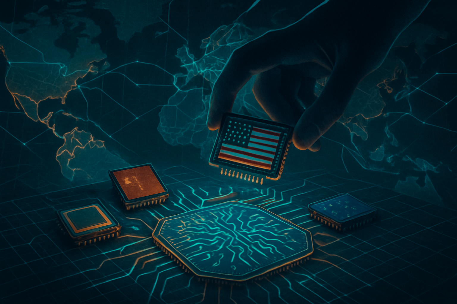
Tag: AI News

  • CVD Equipment Soars as Strategic Order Ignites Silicon Carbide Market, Fueling AI’s Power Demands

    CVD Equipment Soars as Strategic Order Ignites Silicon Carbide Market, Fueling AI’s Power Demands

    Central Islip, NY – October 15, 2025 – CVD Equipment Corporation (NASDAQ: CVV) witnessed a significant surge in its stock price today, jumping 7.6% in premarket trading, following yesterday's announcement of a crucial order for its advanced semiconductor systems. The company secured a deal to supply two PVT150 Physical Vapor Transport Systems to Stony Brook University (SBU) for its newly established "onsemi Silicon Carbide Crystal Growth Center." This strategic move underscores the escalating global demand for high-performance, energy-efficient power semiconductors, particularly silicon carbide (SiC) and other wide band gap (WBG) materials, which are becoming indispensable for the foundational infrastructure of artificial intelligence and the accelerating electrification trend.

    The order, placed by SBU with support from onsemi (NASDAQ: ON), signals a critical investment in research and development that directly impacts the future of AI hardware. As AI models grow in complexity and data centers consume ever-increasing amounts of power, the efficiency of underlying semiconductor components becomes paramount. Silicon carbide offers superior thermal management and power handling capabilities compared to traditional silicon, making it a cornerstone technology for advanced power electronics required by AI accelerators, electric vehicles, and renewable energy systems. This latest development from CVD Equipment not only boosts the company's market standing but also highlights the intense innovation driving the semiconductor manufacturing equipment sector to meet the insatiable appetite for AI-ready chips.

    Unpacking the Technological Leap: Silicon Carbide's Rise in AI Infrastructure

    The core of CVD Equipment's recent success lies in its PVT150 Physical Vapor Transport Systems, specialized machines designed for the intricate process of growing silicon carbide crystals. These systems are critical for creating the high-quality SiC boules that are then sliced into wafers, forming the basis of SiC power semiconductors. The collaboration with Stony Brook University's onsemi Silicon Carbide Crystal Growth Center emphasizes a forward-looking approach, aiming to advance the science of SiC crystal growth and explore other wide band gap materials. Initially, these PVT systems will be installed at CVD Equipment’s headquarters, allowing SBU students hands-on experience and accelerating research while the university’s dedicated facility is completed.

    Silicon carbide distinguishes itself from conventional silicon by offering higher breakdown voltage, faster switching speeds, and superior thermal conductivity. These properties are not merely incremental improvements; they represent a step-change in efficiency and performance crucial for applications where power loss and heat generation are significant concerns. For AI, this translates into more efficient power delivery to GPUs and specialized AI accelerators, reducing operational costs and enabling denser computing environments. Unlike previous generations of power semiconductors, SiC can operate at higher temperatures and frequencies, making it ideal for the demanding environments of AI data centers, 5G infrastructure, and electric vehicle powertrains. The industry's positive reaction to CVD Equipment's order reflects a clear recognition of SiC's pivotal role, despite the company's current financial metrics showing operating challenges, analysts remain optimistic about the long-term growth trajectory in this specialized market. CVD Equipment is also actively developing 200 mm SiC crystal growth processes with its PVT200 systems, anticipating even greater demand from the high-power electronics industry.

    Reshaping the AI Hardware Ecosystem: Beneficiaries and Competitive Dynamics

    This significant order for CVD Equipment reverberates across the entire AI hardware ecosystem. Companies heavily invested in AI development and deployment stand to benefit immensely from the enhanced availability and performance of silicon carbide semiconductors. Chip designers like NVIDIA (NASDAQ: NVDA) and AMD (NASDAQ: AMD), whose GPUs and AI accelerators power the vast majority of AI workloads, will find more robust and efficient power delivery solutions for their next-generation products. This directly impacts the ability of tech giants such as Amazon (NASDAQ: AMZN), Microsoft (NASDAQ: MSFT), and Google (NASDAQ: GOOGL) to scale their cloud AI services with greater energy efficiency and reduced operational costs in their massive data centers.

    The competitive landscape among semiconductor equipment manufacturers is also heating up. While CVD Equipment secures a niche in SiC crystal growth, larger players like Applied Materials (NASDAQ: AMAT) and Lam Research (NASDAQ: LRCX) are also investing heavily in advanced materials and deposition technologies. This order helps CVD Equipment solidify its position as a key enabler for SiC technology. For startups developing AI hardware or specialized power management solutions, the advancements in SiC manufacturing mean access to more powerful and compact components, potentially disrupting existing product lines that rely on less efficient silicon-based power electronics. The strategic advantage lies with companies that can leverage these advanced materials to deliver superior performance and energy efficiency, a critical differentiator in the increasingly competitive AI market.

    Wider Significance: A Bellwether for AI's Foundational Shift

    CVD Equipment's order is more than just a win for a single company; it serves as a powerful indicator of the broader trends shaping the semiconductor industry and, by extension, the future of AI. The escalating demand for advanced semiconductor devices in 5G infrastructure, the Internet of Things (IoT), and particularly artificial intelligence, is driving unprecedented growth in the manufacturing equipment sector. Silicon carbide and other wide band gap materials are at the forefront of this revolution, addressing the fundamental power and efficiency challenges that traditional silicon is increasingly unable to meet.

    This development fits perfectly into the narrative of AI's relentless pursuit of computational power and energy efficiency. As AI models become larger and more complex, requiring immense computational resources, the underlying hardware must evolve in lockstep. SiC power semiconductors are a crucial part of this evolution, enabling the efficient power conversion and management necessary for high-performance computing clusters. The semiconductor CVD equipment market is projected to reach USD 24.07 billion by 2030, growing at a Compound Annual Growth Rate (CAGR) of 5.95% from 2025, underscoring the long-term significance of this sector. While potential concerns regarding future oversupply or geopolitical impacts on supply chains always loom, the current trajectory suggests a robust and sustained demand, reminiscent of previous semiconductor booms driven by personal computing and mobile revolutions, but now fueled by AI.

    The Road Ahead: Scaling Innovation for AI's Future

    Looking ahead, the momentum generated by orders like CVD Equipment's is expected to drive further innovation and expansion in the silicon carbide and wider semiconductor manufacturing equipment markets. Near-term developments will likely focus on scaling production capabilities for SiC wafers, improving crystal growth yields, and reducing manufacturing costs to make these advanced materials more accessible. The collaboration between industry and academia, as exemplified by the Stony Brook-onsemi partnership, will be vital for accelerating fundamental research and training the next generation of engineers.

    Long-term, the applications of SiC and WBG materials are poised to expand beyond power electronics into areas like high-frequency communications and even quantum computing components, where their unique properties can offer significant advantages. However, challenges remain, including the high capital expenditure required for R&D and manufacturing facilities, and the need for a skilled workforce capable of operating and maintaining these sophisticated systems. Experts predict a sustained period of growth for the semiconductor equipment sector, with AI acting as a primary catalyst, continually pushing the boundaries of what's possible in chip design and material science. The focus will increasingly shift towards integrated solutions that optimize power, performance, and thermal management for AI-specific workloads.

    A New Era for AI's Foundational Hardware

    CVD Equipment's stock jump, triggered by a strategic order for its silicon carbide systems, marks a significant moment in the ongoing evolution of AI's foundational hardware. The key takeaway is clear: the demand for highly efficient, high-performance power semiconductors, particularly those made from silicon carbide and other wide band gap materials, is not merely a trend but a fundamental requirement for the continued advancement and scalability of artificial intelligence. This development underscores the critical role that specialized equipment manufacturers play in enabling the next generation of AI-powered technologies.

    This event solidifies the importance of material science innovation in the AI era, highlighting how breakthroughs in seemingly niche areas can have profound impacts across the entire technology landscape. As AI continues its rapid expansion, the focus will increasingly be on the efficiency and sustainability of its underlying infrastructure. We should watch for further investments in SiC and WBG technologies, new partnerships between equipment manufacturers, chipmakers, and research institutions, and the overall financial performance of companies like CVD Equipment as they navigate this exciting, yet challenging, growth phase. The future of AI is not just in algorithms and software; it is deeply intertwined with the physical limits and capabilities of the chips that power it.


    This content is intended for informational purposes only and represents analysis of current AI developments.

    TokenRing AI delivers enterprise-grade solutions for multi-agent AI workflow orchestration, AI-powered development tools, and seamless remote collaboration platforms.
    For more information, visit https://www.tokenring.ai/.

  • GigaDevice and Navitas Forge Joint Lab to Electrify the Future of High-Efficiency AI and EV Power Management

    GigaDevice and Navitas Forge Joint Lab to Electrify the Future of High-Efficiency AI and EV Power Management

    Shanghai, China – October 15, 2025 – In a significant move poised to redefine power management across critical sectors, GigaDevice (SSE: 603986), a global leader in microcontrollers and flash memory, and Navitas Semiconductor (NASDAQ: NVTS), a pioneer in Gallium Nitride (GaN) power integrated circuits, officially launched their joint lab initiative on April 9, 2025. This strategic collaboration, formally announced following a signing ceremony in Shanghai on April 8, 2025, is dedicated to accelerating the deployment of high-efficiency power management solutions, with a keen focus on integrating GaNFast™ ICs and advanced microcontrollers (MCUs) for applications ranging from AI data centers to electric vehicles (EVs) and renewable energy systems. The partnership marks a pivotal step towards a greener, more intelligent era of digital power.

    The primary objective of this joint venture is to overcome the inherent complexities of designing with next-generation power semiconductors like GaN and Silicon Carbide (SiC). By combining Navitas’ cutting-edge wide-bandgap (WBG) power devices with GigaDevice’s sophisticated control capabilities, the lab aims to deliver optimized, system-level solutions that maximize energy efficiency, reduce form factors, and enhance overall performance. This initiative is particularly timely, given the escalating power demands of artificial intelligence infrastructure and the global push for sustainable energy solutions, positioning both companies at the forefront of the high-efficiency power revolution.

    Technical Synergy: Unlocking the Full Potential of GaN and Advanced MCUs

    The technical foundation of the GigaDevice-Navitas joint lab rests on the symbiotic integration of two distinct yet complementary semiconductor technologies. Navitas brings its renowned GaNFast™ power ICs, which boast superior switching speeds and efficiency compared to traditional silicon. These GaN solutions integrate GaN FETs, gate drivers, logic, and protection circuits onto a single chip, drastically reducing parasitic effects and enabling power conversion at much higher frequencies. This translates into power supplies that are up to three times smaller and lighter, with faster charging capabilities, a critical advantage for compact, high-power-density applications. The partnership also extends to SiC technology, another wide-bandgap material offering similar performance enhancements.

    Complementing Navitas' power prowess are GigaDevice's advanced GD32 series microcontrollers, built on the high-performance ARM Cortex-M7 core. These MCUs are vital for providing the precise, high-speed control algorithms necessary to fully leverage the rapid switching characteristics of GaN and SiC devices. Traditional silicon-based power systems operate at lower frequencies, making control relatively simpler. However, the high-frequency operation of GaN demands a sophisticated, real-time control system that can respond instantaneously to optimize performance, manage thermals, and ensure stability. The joint lab will co-develop hardware and firmware, addressing critical design challenges such as EMI reduction, thermal management, and robust protection algorithms, which are often complex hurdles in wide-bandgap power design.

    This integrated approach represents a significant departure from previous methodologies, where power device and control system development often occurred in silos, leading to suboptimal performance and prolonged design cycles. By fostering direct collaboration, the joint lab ensures a seamless handshake between the power stage and the control intelligence, paving the way for unprecedented levels of system integration, energy efficiency, and power density. While specific initial reactions from the broader AI research community were not immediately detailed, the industry's consistent demand for more efficient power solutions for AI workloads suggests a highly positive reception for this strategic convergence of expertise.

    Market Implications: A Competitive Edge in High-Growth Sectors

    The establishment of the GigaDevice-Navitas joint lab carries substantial implications for companies across the technology landscape, particularly those operating in power-intensive domains. Companies poised to benefit immediately include manufacturers of AI servers and data center infrastructure, electric vehicle OEMs, and developers of solar inverters and energy storage systems. The enhanced efficiency and power density offered by the co-developed solutions will allow these industries to reduce operational costs, improve product performance, and accelerate their transition to sustainable technologies.

    For Navitas Semiconductor (NASDAQ: NVTS), this partnership strengthens its foothold in the rapidly expanding Chinese industrial and automotive markets, leveraging GigaDevice's established presence and customer base. It solidifies Navitas' position as a leading innovator in GaN and SiC power solutions by providing a direct pathway for its technology to be integrated into complete, optimized systems. Similarly, GigaDevice (SSE: 603986) gains a significant strategic advantage by enhancing its GD32 MCU offerings with advanced digital power capabilities, a core strategic market for the company. This allows GigaDevice to offer more comprehensive, intelligent system solutions in high-growth areas like EVs and AI, potentially disrupting existing product lines that rely on less integrated or less efficient power management architectures.

    The competitive landscape for major AI labs and tech giants is also subtly influenced. As AI models grow in complexity and size, their energy consumption becomes a critical bottleneck. Solutions that can deliver more power with less waste and in smaller footprints will be highly sought after. This partnership positions both GigaDevice and Navitas to become key enablers for the next generation of AI infrastructure, offering a competitive edge to companies that adopt their integrated solutions. Market positioning is further bolstered by the focus on system-level reference designs, which will significantly reduce time-to-market for new products, making it easier for manufacturers to adopt advanced GaN and SiC technologies.

    Wider Significance: Powering the "Smart + Green" Future

    This joint lab initiative fits perfectly within the broader AI landscape and the accelerating trend towards more sustainable and efficient computing. As AI models become more sophisticated and ubiquitous, their energy footprint grows exponentially. The development of high-efficiency power management is not just an incremental improvement; it is a fundamental necessity for the continued advancement and environmental viability of AI. The "Smart + Green" strategic vision underpinning this collaboration directly addresses these concerns, aiming to make AI infrastructure and other power-hungry applications more intelligent and environmentally friendly.

    The impacts are far-reaching. By enabling smaller, lighter, and more efficient power electronics, the partnership contributes to the reduction of global carbon emissions, particularly in data centers and electric vehicles. It facilitates the creation of more compact devices, freeing up valuable space in crowded server racks and enabling longer ranges or faster charging times for EVs. This development continues the trajectory of wide-bandgap semiconductors, like GaN and SiC, gradually displacing traditional silicon in high-power, high-frequency applications, a trend that has been gaining momentum over the past decade.

    While the research did not highlight specific concerns, the primary challenge for any new technology adoption often lies in cost-effectiveness and mass-market scalability. However, the focus on providing comprehensive system-level designs and reducing time-to-market aims to mitigate these concerns by simplifying the integration process and accelerating volume production. This collaboration represents a significant milestone, comparable to previous breakthroughs in semiconductor integration that have driven successive waves of technological innovation, by directly addressing the power efficiency bottleneck that is becoming increasingly critical for modern AI and other advanced technologies.

    Future Developments and Expert Predictions

    Looking ahead, the GigaDevice-Navitas joint lab is expected to rapidly roll out a suite of comprehensive reference designs and application-specific solutions. In the near term, we can anticipate seeing optimized power modules and control boards specifically tailored for AI server power supplies, EV charging infrastructure, and high-density industrial power systems. These reference designs will serve as blueprints, significantly shortening development cycles for manufacturers and accelerating the commercialization of GaN and SiC in these higher-power markets.

    Longer-term developments could include even tighter integration, potentially leading to highly sophisticated, single-chip solutions that combine power delivery and intelligent control. Potential applications on the horizon include advanced robotics, next-generation renewable energy microgrids, and highly integrated power solutions for edge AI devices. The primary challenges that will need to be addressed include further cost optimization to enable broader market penetration, continuous improvement in thermal management for ultra-high power density, and the development of robust supply chains to support increased demand for GaN and SiC devices.

    Experts predict that this type of deep collaboration between power semiconductor specialists and microcontroller providers will become increasingly common as the industry pushes the boundaries of efficiency and integration. The synergy between high-speed power switching and intelligent digital control is seen as essential for unlocking the full potential of wide-bandbandgap technologies. It is anticipated that the joint lab will not only accelerate the adoption of GaN and SiC but also drive further innovation in related fields such as advanced sensing, protection, and communication within power systems.

    A Crucial Step Towards Sustainable High-Performance Electronics

    In summary, the joint lab initiative by GigaDevice and Navitas Semiconductor represents a strategic and timely convergence of expertise, poised to significantly advance the field of high-efficiency power management. The synergy between Navitas’ cutting-edge GaNFast™ power ICs and GigaDevice’s advanced GD32 series microcontrollers promises to deliver unprecedented levels of energy efficiency, power density, and system integration. This collaboration is a critical enabler for the burgeoning demands of AI data centers, the rapid expansion of electric vehicles, and the global transition to renewable energy sources.

    This development holds profound significance in the history of AI and broader electronics, as it directly addresses one of the most pressing challenges facing modern technology: the escalating need for efficient power. By simplifying the design process and accelerating the deployment of advanced wide-bandgap solutions, the joint lab is not just optimizing power; it's empowering the next generation of intelligent, sustainable technologies.

    As we move forward, the industry will be closely watching for the tangible outputs of this collaboration – the release of new reference designs, the adoption of their integrated solutions by leading manufacturers, and the measurable impact on energy efficiency across various sectors. The GigaDevice-Navitas partnership is a powerful testament to the collaborative spirit driving innovation, and a clear signal that the future of high-performance electronics will be both smart and green.


    This content is intended for informational purposes only and represents analysis of current AI developments.

    TokenRing AI delivers enterprise-grade solutions for multi-agent AI workflow orchestration, AI-powered development tools, and seamless remote collaboration platforms.
    For more information, visit https://www.tokenring.ai/.

  • Geopolitical Fault Lines Reshape Global Chip Industry: Nexperia Case Highlights Tangible Impact of US Regulatory Clampdown

    Geopolitical Fault Lines Reshape Global Chip Industry: Nexperia Case Highlights Tangible Impact of US Regulatory Clampdown

    The global semiconductor industry finds itself at the epicenter of an escalating geopolitical rivalry, with the United States increasingly leveraging regulatory powers to safeguard national security and technological supremacy. This intricate web of export controls, investment screenings, and strategic incentives is creating a challenging operational environment for semiconductor companies worldwide. A prime example of these tangible effects is the unfolding saga of Nexperia, a Dutch-incorporated chipmaker ultimately owned by China's Wingtech Technology, whose recent trajectory illustrates the profound influence of US policy, even when applied indirectly or through allied nations.

    The Nexperia case, culminating in its parent company's addition to the US Entity List in December 2024 and the Dutch government's unprecedented move to take control of Nexperia in late September 2025, serves as a stark warning to companies navigating the treacherous waters of international technology trade. These actions underscore a determined effort by Western nations to decouple critical supply chains from perceived adversaries, forcing semiconductor firms to re-evaluate their global strategies, supply chain resilience, and corporate governance in an era defined by technological nationalism.

    Regulatory Mechanisms and Their Far-Reaching Consequences

    The US approach to securing its semiconductor interests is multi-faceted, employing a combination of direct export controls, inbound investment screening, and outbound investment restrictions. These mechanisms, while often aimed at specific entities or technologies, cast a wide net, impacting the entire global semiconductor value chain.

    The Committee on Foreign Investment in the United States (CFIUS) has long been a gatekeeper for foreign investments into US businesses deemed critical for national security. While CFIUS did not directly review Nexperia's acquisition of the UK's Newport Wafer Fab (NWF), its consistent blocking of Chinese acquisitions of US semiconductor firms (e.g., Lattice Semiconductor in 2017, Magnachip Semiconductor in 2021) established a clear precedent. This US stance significantly influenced the UK government's decision to intervene in the NWF deal. Nexperia's acquisition of NWF in July 2021, the UK's largest chip plant, quickly drew scrutiny. By April 2022, the US House of Representatives' China Task Force formally urged President Joe Biden to pressure the UK to block the deal, citing Wingtech's Chinese ownership and the strategic importance of semiconductors. This pressure culminated in the UK government, under its National Security and Investment Act 2021, ordering Nexperia to divest 86% of its stake in NWF on November 18, 2022. Subsequently, in November 2023, Nexperia sold NWF to US-based Vishay Intertechnology (NYSE: VSH) for $177 million, effectively reversing the controversial acquisition.

    Beyond investment screening, direct US export controls have become a powerful tool. The US Department of Commerce's Bureau of Industry and Security (BIS) added Nexperia's parent company, Wingtech, to its "Entity List" in December 2024. This designation prohibits US companies from exporting or transferring US-origin goods, software, or technology to Wingtech and its subsidiaries, including Nexperia, without a special license, which is often denied. The rationale cited was Wingtech's alleged role in "aiding China's government's efforts to acquire entities with sensitive semiconductor manufacturing capability." This move significantly restricts Nexperia's access to crucial US technology and equipment, forcing the company to seek alternative suppliers and re-engineer its processes, incurring substantial costs and operational delays. The US has further expanded these restrictions, notably through rules introduced in October 2022 and October 2023, which tighten controls on high-end chips (including AI chips), semiconductor manufacturing equipment (SME), and "US persons" supporting Chinese chip production, with explicit measures to target circumvention.

    Adding another layer of complexity, the US CHIPS and Science Act, enacted in August 2022, provides billions in federal funding for domestic semiconductor manufacturing but comes with "guardrails." Companies receiving these funds are prohibited for 10 years from engaging in "significant transactions" involving the material expansion of semiconductor manufacturing capacity in "foreign countries of concern" like China. This effectively creates an outbound investment screening mechanism, aligning global investment strategies with US national security priorities. The latest development, publicly announced on October 12, 2025, saw the Dutch government invoke its Cold War-era "Goods Availability Act" on September 30, 2025, to take control of Nexperia. This "highly exceptional" move, influenced by the broader geopolitical climate and US pressures, cited "recent and acute signals of serious governance shortcomings" at Nexperia, aiming to safeguard crucial technological knowledge and ensure the availability of essential chips for European industries. The Dutch court suspended Nexperia's Chinese CEO and transferred Wingtech's 99% stake to an independent trustee, marking an unprecedented level of government intervention in a private company due to geopolitical concerns.

    Competitive Implications and Market Realignments

    The intensified regulatory environment and the Nexperia case send clear signals across the semiconductor landscape, prompting a re-evaluation of strategies for tech giants, startups, and national economies alike.

    US-based semiconductor companies such as Intel (NASDAQ: INTC), Qualcomm (NASDAQ: QCOM), and NVIDIA (NASDAQ: NVDA) stand to benefit from the CHIPS Act's incentives for domestic manufacturing, bolstering their capabilities within US borders. However, they also face the challenge of navigating export controls, which can limit their market access in China, a significant consumer of chips. NVIDIA, for instance, has had to design specific chips to comply with restrictions on advanced AI accelerators for the Chinese market. Companies like Vishay Intertechnology (NYSE: VSH), by acquiring assets like Newport Wafer Fab, demonstrate how US regulatory actions can facilitate the strategic acquisition of critical manufacturing capabilities by Western firms.

    For major non-US chip manufacturers like Taiwan Semiconductor Manufacturing Company (TSMC) (NYSE: TSM) and Samsung (KRX: 005930), the competitive implications are complex. While they may gain from increased demand from Western customers seeking diversified supply chains, they also face immense pressure to establish manufacturing facilities in the US and Europe to qualify for subsidies and mitigate geopolitical risks. This necessitates massive capital expenditures and operational adjustments, potentially impacting their profitability and global market share in the short term. Meanwhile, Chinese semiconductor companies, including Nexperia's parent Wingtech, face significant disruption. The Entity List designation severely curtails their access to advanced US-origin technology, equipment, and software, hindering their ability to innovate and compete at the leading edge. Wingtech announced in March 2025 a spin-off of a major part of its operations to focus on semiconductors, explicitly citing the "geopolitical environment" as a driving factor, highlighting the strategic shifts forced upon companies caught in the crossfire.

    The potential disruption to existing products and services is substantial. Companies relying on a globally integrated supply chain, particularly those with significant exposure to Chinese manufacturing or R&D, must now invest heavily in diversification and localization. This could lead to higher production costs, slower innovation cycles due to restricted access to best-in-class tools, and potential delays in product launches. Market positioning is increasingly influenced by geopolitical alignment, with "trusted" supply chains becoming a key strategic advantage. Companies perceived as aligned with Western national security interests may gain preferential access to markets and government contracts, while those with ties to "countries of concern" face increasing barriers and scrutiny. This trend is compelling startups to consider their ownership structures and funding sources more carefully, as venture capital from certain regions may become a liability rather than an asset in critical technology sectors.

    The Broader AI Landscape and Geopolitical Realities

    The Nexperia case and the broader US regulatory actions are not isolated incidents but rather integral components of a larger geopolitical struggle for technological supremacy, particularly in artificial intelligence. Semiconductors are the foundational bedrock of AI, powering everything from advanced data centers to edge devices. Control over chip design, manufacturing, and supply chains is therefore synonymous with control over the future of AI.

    These actions fit into a broader trend of "de-risking" or "decoupling" critical technology supply chains, driven by national security concerns and a desire to reduce dependency on geopolitical rivals. The impacts extend beyond individual companies to reshape global trade flows, investment patterns, and technological collaboration. The push for domestic manufacturing, exemplified by the CHIPS Act in the US and similar initiatives like the EU Chips Act, aims to create resilient regional ecosystems, but at the cost of global efficiency and potentially fostering a more fragmented, less innovative global AI landscape.

    Potential concerns include the risk of economic nationalism spiraling into retaliatory measures, where countries impose their own restrictions on technology exports or investments, further disrupting global markets. China's export restrictions on critical minerals like gallium and germanium in July 2023 serve as a stark reminder of this potential. Such actions could lead to a balkanization of the tech world, with distinct technology stacks and standards emerging in different geopolitical blocs, hindering global interoperability and the free flow of innovation. This compares to previous AI milestones where the focus was primarily on technological breakthroughs and ethical considerations; now, the geopolitical dimension has become equally, if not more, dominant. The race for AI leadership is no longer just about who has the best algorithms but who controls the underlying hardware infrastructure and the rules governing its development and deployment.

    Charting Future Developments in a Fractured World

    The trajectory of US regulatory actions and their impact on semiconductor companies like Nexperia indicates a future marked by continued strategic competition and a deepening divide in global technology ecosystems.

    In the near term, we can expect further tightening of export controls, particularly concerning advanced AI chips and sophisticated semiconductor manufacturing equipment. The US Department of Commerce is likely to expand its Entity List to include more companies perceived as supporting rival nations' military or technological ambitions. Allied nations, influenced by US policy and their own national security assessments, will likely enhance their investment screening mechanisms and potentially implement similar export controls, as seen with the Dutch government's recent intervention in Nexperia. The "guardrails" of the CHIPS Act will become more rigidly enforced, compelling companies to make definitive choices about where they expand their manufacturing capabilities.

    Long-term developments will likely involve the emergence of parallel, less interdependent semiconductor supply chains. This "friend-shoring" or "ally-shoring" will see increased investment in manufacturing and R&D within politically aligned blocs, even if it comes at a higher cost. We may also see an acceleration in the development of "non-US origin" alternatives for critical semiconductor tools and materials, particularly in China, as a direct response to export restrictions. This could lead to a divergence in technological standards and architectures over time. Potential applications and use cases on the horizon will increasingly be influenced by these geopolitical considerations; for instance, the development of AI for defense applications will be heavily scrutinized for supply chain integrity.

    The primary challenges that need to be addressed include maintaining global innovation in a fragmented environment, managing the increased costs associated with diversified and localized supply chains, and preventing a full-scale technological cold war that stifles progress for all. Experts predict that companies will continue to face immense pressure to choose sides, even implicitly, through their investment decisions, supply chain partners, and market focus. The ability to navigate these complex geopolitical currents, rather than just technological prowess, will become a critical determinant of success in the semiconductor and AI industries. What experts predict is a sustained period of strategic competition, where national security concerns will continue to override purely economic considerations in critical technology sectors.

    A New Era of Geopolitical Tech Warfare

    The Nexperia case stands as a powerful testament to the tangible and far-reaching effects of US regulatory actions on the global semiconductor industry. From the forced divestment of Newport Wafer Fab to the placement of its parent company, Wingtech, on the Entity List, and most recently, the Dutch government's unprecedented move to take control of Nexperia, the narrative highlights a profound shift in how technology, particularly semiconductors, is viewed and controlled in the 21st century.

    This development marks a significant inflection point in AI history, underscoring that the race for artificial intelligence leadership is inextricably linked to the geopolitical control of its foundational hardware. The era of purely economic globalization in critical technologies is giving way to one dominated by national security imperatives and strategic competition. Key takeaways include the increasing extraterritorial reach of US regulations, the heightened scrutiny on foreign investments in critical tech, and the immense pressure on companies to align their operations with national security objectives, often at the expense of market efficiency.

    The long-term impact will likely be a more resilient but also more fragmented global semiconductor ecosystem, characterized by regional blocs and diversified supply chains. While this may reduce dependencies on specific geopolitical rivals, it also risks slowing innovation and increasing costs across the board. What to watch for in the coming weeks and months includes further expansions of export controls, potential retaliatory measures from targeted nations, and how other allied governments respond to similar cases of foreign ownership in their critical technology sectors. The Nexperia saga is not an anomaly but a blueprint for the challenges that will define the future of the global tech industry.


    This content is intended for informational purposes only and represents analysis of current AI developments.

    TokenRing AI delivers enterprise-grade solutions for multi-agent AI workflow orchestration, AI-powered development tools, and seamless remote collaboration platforms.
    For more information, visit https://www.tokenring.ai/.

  • SEALSQ and Trusted Semiconductor Solutions Forge Quantum-Secure Future for U.S. Defense

    SEALSQ and Trusted Semiconductor Solutions Forge Quantum-Secure Future for U.S. Defense

    NEW YORK, NY – October 9, 2025 – In a landmark announcement poised to redefine national data security, SEALSQ Corp (NASDAQ: LAES) and Trusted Semiconductor Solutions (TSS) today unveiled a strategic partnership aimed at developing "Made in US" Post-Quantum Cryptography (PQC)-enabled semiconductor solutions. This collaboration, critically timed with the accelerating advancements in quantum computing, targets U.S. defense and government agencies, promising an impenetrable shield against future quantum threats and marking a pivotal moment in the race for quantum resilience.

    The alliance is set to deliver hardware with the highest level of security certifications, designed to withstand the unprecedented cryptographic challenges posed by cryptographically relevant quantum computers (CRQCs). This initiative is not merely about upgrading existing security but about fundamentally rebuilding the digital trust infrastructure from the ground up, ensuring the confidentiality and integrity of the nation's most sensitive data for decades to come.

    A New Era of Hardware-Level Quantum Security

    The partnership leverages SEALSQ's pioneering expertise in quantum-resistant technology, including its secure microcontrollers and NIST-standardized PQC solutions, with TSS's unparalleled capabilities in high-reliability semiconductor design and its Category 1A Trusted accreditation for classified microelectronics. This synergy is critical for embedding quantum-safe algorithms directly into hardware, offering a robust "root of trust" that software-only solutions cannot guarantee.

    At the heart of this development is SEALSQ's Quantum Shield QS7001 secure element, a chip meticulously engineered to embed NIST-standardized quantum-resistant algorithms (ML-KEM and ML-DSA) at the hardware level. This revolutionary component, slated for launch in mid-November 2025 with commercial development kits available the same month, will provide robust protection for critical applications ranging from defense systems to vital infrastructure. The collaboration also anticipates the release of a QVault Trusted Platform Module (TPM) version in the first half of 2026, further extending hardware-based quantum security.

    This approach differs significantly from previous cryptographic transitions, which often relied on software patches or protocol updates. By integrating PQC directly into the semiconductor architecture, the partnership aims to create tamper-resistant, immutable security foundations. This hardware-centric strategy is essential for secure key storage and management, true random number generation (TRNG) crucial for strong cryptography, and protection against sophisticated supply chain and side-channel attacks. Initial reactions from cybersecurity experts underscore the urgency and foresight of this hardware-first approach, recognizing it as a necessary step to future-proof critical systems against the looming "Q-Day."

    Reshaping the Tech Landscape: Benefits and Competitive Edge

    This strategic alliance between SEALSQ (NASDAQ: LAES) and Trusted Semiconductor Solutions is set to profoundly impact various sectors of the tech industry, particularly those with stringent security requirements. The primary beneficiaries will be U.S. defense and government agencies, which face an immediate and critical need to protect classified information and critical infrastructure from state-sponsored quantum attacks. The "Made in US" aspect, combined with TSS's Category 1A Trusted accreditation, provides an unparalleled level of assurance and compliance with Department of Defense (DoD) and federal requirements, offering a sovereign solution to a global threat.

    For tech giants like Alphabet (NASDAQ: GOOGL), Microsoft (NASDAQ: MSFT), and International Business Machines (NYSE: IBM), who are already heavily invested in quantum computing research and quantum-safe cryptography, this partnership reinforces the industry's direction towards hardware-level security. While these companies are developing their own PQC solutions for cloud services and enterprise products, the SEALSQ-TSS collaboration highlights a specialized, high-assurance pathway for government and defense applications, potentially setting a benchmark for future secure hardware design. Semiconductor manufacturers like NXP Semiconductors (NASDAQ: NXPI) and Taiwan Semiconductor Manufacturing (NYSE: TSM) are also poised to benefit from the growing demand for PQC-enabled chips.

    The competitive implications are significant. Companies that proactively adopt and integrate these quantum-secure chips will gain a substantial strategic advantage, particularly in sectors where data integrity and national security are paramount. This development could disrupt existing cybersecurity product lines that rely solely on classical encryption, forcing a rapid migration to quantum-resistant alternatives. Startups specializing in quantum cryptography, quantum key distribution (QKD), and quantum random number generation (QRNG), such as KETS and Quantum Numbers Corp, will find an expanding market for their complementary technologies as the ecosystem for quantum security matures. SEALSQ itself, through its "Quantum Corridor" initiative and investments in pioneering startups, is actively fostering this burgeoning quantum-resilient world.

    Broader Significance: Securing the Digital Frontier

    The partnership between SEALSQ and Trusted Semiconductor Solutions is a critical milestone in the broader AI and cybersecurity landscape, directly addressing one of the most significant threats to modern digital infrastructure: the advent of cryptographically relevant quantum computers (CRQCs). These powerful machines, though still in development, possess the theoretical capability to break widely used public-key encryption algorithms like RSA and ECC, which form the bedrock of secure communications, financial transactions, and data protection globally. This initiative squarely tackles the "harvest now, decrypt later" threat, where adversaries could collect encrypted data today and decrypt it in the future once CRQCs become available.

    The impacts of this development extend far beyond defense. In the financial sector, where billions of transactions rely on vulnerable encryption, quantum-secure chips promise impenetrable data encryption for banking, digital signatures, and customer data, preventing catastrophic fraud and identity theft. Healthcare, handling highly sensitive patient records, will benefit from robust protection for telemedicine platforms and data sharing. Critical infrastructure, including energy grids, transportation, and telecommunications, will gain enhanced resilience against cyber-sabotage. The integration of PQC into hardware provides a foundational layer of security that will safeguard these vital systems against the most advanced future threats.

    Potential concerns include the complexity and cost of migrating existing systems to quantum-safe hardware, the ongoing evolution of quantum algorithms, and the need for continuous standardization. However, the proactive nature of this partnership, aligning with NIST's PQC standardization process, mitigates some of these risks. This collaboration stands as a testament to the industry's commitment to staying ahead of the quantum curve, drawing comparisons to previous cryptographic milestones that secured the internet in its nascent stages.

    The Road Ahead: Future-Proofing Our Digital World

    Looking ahead, the partnership outlines a clear three-phase development roadmap. The immediate focus is on integrating SEALSQ's QS7001 secure element into TSS's trusted semiconductor platforms, with the chip's launch anticipated in mid-November 2025. This will be followed by the co-development of "Made in US" PQC-embedded Integrated Circuits (ICs) aiming for stringent FIPS 140-3, Common Criteria, and specific agency certifications. The long-term vision includes the development of next-generation secure architectures, such as Chiplet-based Hardware Security Modules (CHSMs) with advanced embedded secure elements, promising a future where digital assets are protected by an unassailable hardware-rooted trust.

    The potential applications and use cases on the horizon are vast. Beyond defense, these quantum-secure chips could find their way into critical infrastructure, IoT devices, automotive systems, and financial networks, providing a new standard of security for data in transit and at rest. Experts predict a rapid acceleration in the adoption of hardware-based PQC solutions, driven by regulatory mandates and the escalating threat landscape. The ongoing challenge will be to ensure seamless integration into existing ecosystems and to maintain agility in the face of evolving quantum computing capabilities.

    What experts predict will happen next is a surge in demand for quantum-resistant components and a race among nations and corporations to secure their digital supply chains. This partnership positions the U.S. at the forefront of this crucial technological arms race, providing sovereign capabilities in quantum-secure microelectronics.

    A Quantum Leap for Cybersecurity

    The partnership between SEALSQ and Trusted Semiconductor Solutions represents a monumental leap forward in cybersecurity. By combining SEALSQ's innovative quantum-resistant technology with TSS's trusted manufacturing and accreditation, the alliance is delivering a tangible, hardware-based solution to the existential threat posed by quantum computing. The immediate significance lies in its direct application to U.S. defense and government agencies, providing an uncompromised level of security for national assets.

    This development will undoubtedly be remembered as a critical juncture in AI and cybersecurity history, marking the transition from theoretical quantum threat mitigation to practical, deployable quantum-secure hardware. It underscores the urgent need for proactive measures and collaborative innovation to safeguard our increasingly digital world.

    In the coming weeks and months, the tech community will be closely watching the launch of the QS7001 chip and the subsequent phases of this partnership. Its success will not only secure critical U.S. infrastructure but also set a precedent for global quantum resilience efforts, ushering in a new era of trust and security in the digital age.


    This content is intended for informational purposes only and represents analysis of current AI developments.
    TokenRing AI delivers enterprise-grade solutions for multi-agent AI workflow orchestration, AI-powered development tools, and seamless remote collaboration platforms. For more information, visit https://www.tokenring.ai/.

  • India’s Silicon Dream: Modi’s ‘Make in India’ Propels Nation Towards Semiconductor and Electronics Self-Reliance

    India’s Silicon Dream: Modi’s ‘Make in India’ Propels Nation Towards Semiconductor and Electronics Self-Reliance

    India is on the cusp of a technological revolution, driven by Prime Minister Narendra Modi's ambitious "Make in India" initiative, which has strategically pivoted towards establishing the nation as a formidable global hub for semiconductor and electronics manufacturing. With a keen eye on reducing import dependency and fostering technological sovereignty, the government has unleashed a torrent of policies and incentives designed to attract significant domestic and foreign investment. As of October 2025, India is witnessing the tangible fruits of these efforts, with the first domestically produced semiconductor chips poised to roll out, marking a pivotal moment in the country's journey to become a self-reliant powerhouse in the digital age. This concerted push aims to integrate India more deeply into the global technology supply chain, moving beyond its traditional role as a design and software services provider to a key player in hardware production.

    Unprecedented Policy Push and Manufacturing Milestones

    The "Make in India" initiative, launched in September 2014, has evolved significantly, with its technological arm now laser-focused on an aggressive timeline to achieve self-sufficiency in electronics and semiconductor production. The goals are starkly ambitious: achieve a domestic electronics production target of USD 300 billion by 2026, escalating to USD 500 billion by 2030-31, and increasing domestic value addition to 30-35%. In the semiconductor realm, the aim is to expand India's market from approximately $15 billion in 2021 to over $100 billion by 2026, ultimately targeting a valuation of $100-110 billion by 2030.

    Central to this push is a robust framework of government policies, spearheaded by the Production Linked Incentive (PLI) scheme, launched in 2020. This scheme offers financial incentives ranging from 3% to 6% on incremental sales of goods manufactured in India, proving particularly attractive to the electronics sector. The impact has been profound, with local mobile phone production skyrocketing from 26% in 2014-15 to an astounding 99.2% by December 2024. Further bolstering this ecosystem is the India Semiconductor Mission (ISM), launched in December 2021 with an initial outlay of ₹76,000 crore (approximately $9.2 billion), specifically designed to foster a comprehensive semiconductor and display manufacturing ecosystem. The Electronics Components Manufacturing Scheme (ECMS), notified in April 2025 with an outlay of ₹22,919 crore (US$2.7 billion), further targets reducing import dependency for electronic components.

    Significant strides have been made under the ISM. Notably, in June 2023, the Indian cabinet approved a substantial US$2.7 billion investment plan by Micron Technology (NASDAQ: MU) to establish a semiconductor Assembly, Testing, Marking, and Packaging (ATMP) unit in Gujarat. Following this, February 2024 saw the government greenlight Tata Electronics' (NSE: TATAEL) proposal to build a mega semiconductor fabrication facility in Dholera, Gujarat, in partnership with Taiwan's Powerchip Semiconductor Manufacturing Corporation (PSMC), with an investment of ₹91,000 crore (approximately $11 billion). As of October 2025, test chips from companies like Micron and Tata Electronics are already in production, with Tata Electronics and PSMC anticipated to launch India's first commercially produced "Made-in-India" chip from their Dholera plant between September and October 2025. This rapid progression marks a significant departure from previous approaches, which primarily focused on design rather than end-to-end manufacturing, positioning India as a serious contender in the global chip fabrication landscape. The recent inauguration of CG Power's (NSE: CGPOWER) end-to-end Semiconductor OSAT Pilot Line Facility in Sanand, Gujarat, in August 2025, further cements India's growing capabilities in advanced packaging.

    Shifting Tides: Impact on Global and Domestic Players

    The aggressive "Make in India" push in semiconductors and electronics is reshaping the competitive landscape for both domestic and international companies. Global giants like Micron Technology (NASDAQ: MU) are among the first to directly benefit, leveraging government incentives and India's burgeoning market to establish critical manufacturing footholds. Their ATMP unit in Gujarat is not just an investment but a strategic move to diversify global supply chains and tap into India's growing talent pool, potentially leading to significant operational efficiencies and market access.

    Domestically, the initiative is catalyzing the emergence of new players and empowering established conglomerates. Tata Electronics (NSE: TATAEL), a subsidiary of the Tata Group (NSE: TATAMOTORS), is making a monumental entry into chip fabrication, signaling a strategic pivot towards high-tech manufacturing. Its partnership with PSMC brings invaluable expertise, allowing Tata to leapfrog years of development. Similarly, the joint venture between HCL (NSE: HCLTECH) and Foxconn (TWSE: 2354) for a semiconductor plant near Jewar Airport highlights a collaborative model designed to accelerate production and technology transfer. Companies like CG Power (NSE: CGPOWER) and Kaynes SemiCon (NSE: KAYNES), establishing OSAT facilities, are crucial for creating an integrated ecosystem, reducing reliance on foreign packaging services.

    This surge in domestic production capability poses both opportunities and challenges. While it promises to reduce India's import bill and create millions of jobs, it also intensifies competition in the global market. Existing technology giants that have traditionally viewed India primarily as a consumption market or a software development hub are now being compelled to consider deeper manufacturing investments to maintain relevance and competitive advantage. The initiative has the potential to disrupt existing supply chain dynamics, offering an alternative manufacturing base outside of traditional Asian powerhouses and potentially leading to a more resilient global electronics industry.

    Broader Implications: Geopolitics, Self-Reliance, and Global Trends

    India's "Make in India" initiative, particularly its laser focus on semiconductors and electronics, transcends mere economic ambition; it is a strategic play with profound geopolitical implications. In an era marked by increasing supply chain vulnerabilities and technological nationalism, India's quest for self-reliance in critical technologies positions it as a more resilient and influential player on the global stage. This move aligns with broader global trends where nations are scrambling to secure their semiconductor supply chains, as evidenced by similar initiatives in the US (CHIPS Act) and Europe.

    The impact of this initiative extends to national security, as domestic production of essential components reduces reliance on potentially hostile foreign sources. It also bolsters India's digital economy, which is increasingly dependent on advanced electronics. By fostering a robust manufacturing base, India aims to move up the technology value chain, transitioning from a consumer of technology to a producer and innovator. This is a significant shift from previous decades, where India primarily focused on software and IT services, often importing the hardware infrastructure.

    However, potential concerns remain. Building a world-class semiconductor ecosystem requires not only massive capital investment but also a highly skilled workforce, reliable infrastructure (power, water), and a robust R&D pipeline. While government policies are addressing capital, the long-term success will hinge on India's ability to rapidly scale its talent pool and create an environment conducive to cutting-edge research and innovation. Comparisons to previous AI milestones, such as the development of large language models, highlight the importance of sustained investment in foundational research and talent development to truly become a global leader. The initiative's success could also inspire other developing nations to pursue similar paths towards technological independence.

    The Road Ahead: Future Developments and Challenges

    The immediate future for India's semiconductor and electronics sectors looks incredibly promising. With the first indigenous chips expected to roll out commercially by the end of 2025, the focus will shift towards scaling production, attracting more advanced fabrication technologies, and expanding the ecosystem to include a wider array of components. The India Semiconductor Mission's initial funding of ₹76,000 crore is nearly fully committed, and plans for a second phase are already underway, indicating sustained government support. Maharashtra's goal to become India's semiconductor capital by 2030 underscores the competitive zeal among states to attract these high-value investments.

    In the near term, experts predict a continued influx of foreign direct investment, particularly in packaging, testing, and display manufacturing, as these are less capital-intensive than full-fledged fabrication plants and offer quicker returns. The Design Linked Incentive (DLI) Scheme, which supports 23 chip design projects, will be crucial for fostering indigenous intellectual property and moving beyond contract manufacturing. Long-term developments could see India becoming a significant exporter of not just finished electronic goods but also semiconductor components and even advanced logic chips, potentially serving global markets and diversifying the world's supply chain away from its current concentration in East Asia.

    However, significant challenges need to be addressed. The availability of highly skilled engineers and technicians, particularly in advanced manufacturing processes, remains a critical bottleneck. India will need to rapidly expand its educational and vocational training programs to meet this demand. Ensuring uninterrupted power supply, access to ultra-pure water, and a streamlined regulatory environment will also be paramount. What experts predict next is a period of intense capacity building and technological absorption, with India gradually moving towards more complex and smaller node manufacturing, potentially even venturing into cutting-edge research for next-generation materials and chip architectures.

    A New Era of Indian Manufacturing: Wrap-up

    Prime Minister Modi's "Make in India" initiative, with its sharpened focus on semiconductors and electronics, represents a monumental pivot in India's economic and technological trajectory. The journey from a nascent electronics assembly hub to a nation producing its own semiconductor chips in just over a decade is a testament to ambitious policy-making, strategic investments, and a growing confidence in India's manufacturing capabilities. The significant commitments from global players like Micron and domestic titans like Tata, coupled with robust government incentives, underscore the seriousness and potential of this endeavor.

    This development holds immense significance in AI history, as semiconductors are the bedrock of all AI advancements. By securing its own chip supply, India is not only ensuring its economic future but also laying the groundwork for indigenous AI development and innovation, free from external dependencies. The initiative is poised to create millions of jobs, foster a culture of high-tech manufacturing, and significantly contribute to India's GDP, cementing its position as a global economic power.

    In the coming weeks and months, the world will be watching closely as India's first commercially produced "Made-in-India" chips roll off the production lines. Further investment announcements, progress on talent development, and the performance of initial manufacturing units will be key indicators of the long-term success and sustainability of India's silicon dream. The "Make in India" campaign is no longer just an aspiration; it is rapidly becoming a tangible reality, reshaping global technology landscapes.

    This content is intended for informational purposes only and represents analysis of current AI developments.

    TokenRing AI delivers enterprise-grade solutions for multi-agent AI workflow orchestration, AI-powered development tools, and seamless remote collaboration platforms.
    For more information, visit https://www.tokenring.ai/.

  • The Dual Threat: How Taiwan’s Energy Insecurity and Geopolitical Risks Endanger TSMC and the World’s Tech Future

    The Dual Threat: How Taiwan’s Energy Insecurity and Geopolitical Risks Endanger TSMC and the World’s Tech Future

    Taiwan, the undisputed epicenter of advanced semiconductor manufacturing, finds its critical role in the global technology ecosystem increasingly imperiled by a potent combination of domestic energy insecurity and escalating geopolitical tensions. At the heart of this precarious situation lies Taiwan Semiconductor Manufacturing Company (TSMC) (NYSE: TSM), the world's leading contract chipmaker, whose uninterrupted operation is vital for industries ranging from artificial intelligence and consumer electronics to automotive and defense. The fragility of Taiwan's energy grid, coupled with the ever-present shadow of cross-strait conflict, poses a severe and immediate threat to TSMC's production capabilities, potentially unleashing catastrophic ripple effects across the global economy and significantly impacting the development and deployment of advanced AI technologies.

    The intricate dance between Taiwan's reliance on imported energy and its strategic geopolitical position creates a volatile environment for TSMC, a company that consumes a staggering and growing portion of the island's electricity. Any disruption, whether from a power outage or an external blockade, could cripple the sophisticated and continuous manufacturing processes essential for producing cutting-edge chips. As the world increasingly depends on these advanced semiconductors for everything from smartphones to the data centers powering generative AI, the vulnerabilities facing Taiwan and its silicon champion have become a paramount concern for governments, tech giants, and industries worldwide.

    A Precarious Balance: Energy Demands and Geopolitical Flashpoints

    The technical and operational challenges facing TSMC due to Taiwan's energy situation are profound. Semiconductor fabrication plants (fabs) are among the most energy-intensive industrial facilities globally, requiring a continuous, stable, and high-quality power supply. TSMC's electricity consumption is colossal, projected to reach 10-12% of Taiwan's total usage by 2030, a significant jump from 8% in 2023. This demand is driven by the increasing complexity and power requirements of advanced nodes; for instance, a single 3-nanometer wafer required 40.5 kilowatt-hours of electricity in 2023, more than double that of 10-nanometer chips. The island's energy infrastructure, however, is heavily reliant on imported fossil fuels, with 83% of its power derived from coal, natural gas, and oil, and 97% of its total energy supply being imported. This over-reliance creates a critical vulnerability to both supply chain disruptions and price volatility.

    Taiwan's grid stability has been a recurring concern, marked by significant blackouts in 2021 and 2022 that impacted millions, including TSMC. While TSMC has robust backup systems, even momentary power fluctuations or "brownouts" can damage sensitive equipment and compromise entire batches of wafers, leading to substantial financial losses and production delays. The decommissioning of Taiwan's last operational nuclear reactor in May 2025, a move intended to shift towards renewable energy, has exacerbated these issues, with subsequent power outages pushing the grid's reserve capacity below mandated thresholds. This scenario differs significantly from past energy challenges, where the primary concern was often cost or long-term supply. Today, the immediate threat is the sheer stability and resilience of the grid under rapidly increasing demand, particularly from the booming semiconductor sector, against a backdrop of declining baseload power from nuclear sources and slower-than-anticipated renewable energy deployment.

    Beyond domestic energy woes, the geopolitical landscape casts an even longer shadow. China's assertive stance on Taiwan, viewed as a renegade province, manifests in frequent military exercises in the Taiwan Strait, demonstrating a credible threat of blockade or even invasion. Such actions would immediately sever Taiwan's vital energy imports, especially liquefied natural gas (LNG), which would deplete within weeks, bringing the island's power grid and TSMC's fabs to a standstill. The Strait is also a critical global shipping lane, with 50% of the world's containerships passing through it; any disruption would have immediate and severe consequences for global trade far beyond semiconductors. This differs from previous geopolitical concerns, which might have focused on trade tariffs or intellectual property theft. The current threat involves the physical disruption of manufacturing and supply chains on an unprecedented scale, making the "silicon shield" a double-edged sword that protects Taiwan but also makes it a primary target.

    Initial reactions from the AI research community and industry experts highlight deep concern. Analysts from leading financial institutions have frequently downgraded economic growth forecasts citing potential Taiwan conflict scenarios. Industry leaders, including those from major tech firms, have voiced anxieties over the lack of viable alternatives to TSMC's advanced manufacturing capabilities in the short to medium term. The consensus is that while efforts to diversify chip production globally are underway, no single region or company can replicate TSMC's scale, expertise, and efficiency in producing cutting-edge chips like 3nm and 2nm within the next decade. This makes the current energy and geopolitical vulnerabilities a critical choke point for technological advancement worldwide, particularly for the compute-intensive demands of modern AI.

    Ripples Through the Tech Ecosystem: Who Stands to Lose (and Gain)?

    The potential disruption to TSMC's operations due to energy insecurity or geopolitical events would send shockwaves through the entire technology industry, impacting tech giants, AI companies, and startups alike. Companies that stand to lose the most are those heavily reliant on TSMC for their advanced chip designs. This includes virtually all major players in the high-performance computing and AI space: Apple (NASDAQ: AAPL), which sources the processors for its iPhones and Macs exclusively from TSMC; Nvidia (NASDAQ: NVDA), the dominant force in AI accelerators, whose GPUs are fabricated by TSMC; Qualcomm (NASDAQ: QCOM), a leader in mobile chipsets; and Advanced Micro Devices (NASDAQ: AMD), a key competitor in CPUs and GPUs. Any delay or reduction in TSMC's output would directly translate to product shortages, delayed launches, and significant revenue losses for these companies.

    The competitive implications for major AI labs and tech companies are severe. A prolonged disruption could stifle innovation, as access to the latest, most powerful chips—essential for training and deploying advanced AI models—would become severely restricted. Companies with less diversified supply chains or smaller cash reserves would be particularly vulnerable, potentially losing market share to those with more resilient strategies or alternative sourcing options, however limited. For startups, especially those developing AI hardware or specialized AI chips, such a crisis could be existential, as they often lack the leverage to secure priority allocation from alternative foundries or the resources to absorb significant delays.

    Potential disruption to existing products and services would be widespread. Consumers would face higher prices and limited availability of everything from new smartphones and laptops to gaming consoles and electric vehicles. Data centers, the backbone of cloud computing and AI services, would struggle to expand or even maintain operations without a steady supply of new server processors and AI accelerators. This could lead to a slowdown in AI development, increased costs for AI inference, and a general stagnation in technological progress.

    In terms of market positioning and strategic advantages, the crisis would underscore the urgent need for supply chain diversification. Companies like Intel (NASDAQ: INTC), which is actively expanding its foundry services (Intel Foundry) with significant government backing, might see an opportunity to gain market share, albeit over a longer timeline. However, the immediate impact would be overwhelmingly negative for the industry as a whole. Governments, particularly the U.S. and European Union, would likely accelerate their efforts to incentivize domestic chip manufacturing through initiatives like the CHIPS Act, further reshaping the global semiconductor landscape. This scenario highlights a critical vulnerability in the current globalized tech supply chain, forcing a re-evaluation of just-in-time manufacturing in favor of resilience and redundancy, even at a higher cost.

    The Broader Canvas: AI's Future and Global Stability

    The issues facing TSMC and Taiwan are not merely a supply chain hiccup; they represent a fundamental challenge to the broader AI landscape and global technological trends. Advanced semiconductors are the bedrock upon which modern AI is built. From the massive training runs of large language models to the efficient inference on edge devices, every AI application relies on the continuous availability of cutting-edge chips. A significant disruption would not only slow down the pace of AI innovation but could also create a chasm between the demand for AI capabilities and the hardware required to deliver them. This fits into a broader trend of increasing geopolitical competition over critical technologies, where control over semiconductor manufacturing has become a strategic imperative for nations.

    The impacts would be far-reaching. Economically, a major disruption could trigger a global recession, with estimates suggesting a potential $10 trillion loss to the global economy in the event of a full-scale conflict, or a 2.8% decline in global economic output from a Chinese blockade alone in the first year. Technologically, it could lead to a period of "AI stagnation," where progress slows due to hardware limitations, potentially undermining the anticipated benefits of AI across various sectors. Militarily, it could impact national security, as advanced chips are crucial for defense systems, intelligence gathering, and cyber warfare capabilities.

    Potential concerns extend beyond immediate economic fallout. The concentration of advanced chip manufacturing in Taiwan has long been recognized as a single point of failure. The current situation highlights the fragility of this model and the potential for a cascading failure across interdependent global systems. Comparisons to previous AI milestones and breakthroughs underscore the current predicament. Past advancements, from deep learning to transformer architectures, have been fueled by increasing computational power. A constraint on this power would be a stark contrast to the continuous exponential growth that has characterized AI's progress. While past crises might have involved specific component shortages (e.g., during the COVID-19 pandemic), the current threat to TSMC represents a systemic risk to the foundational technology itself, potentially leading to a more profound and sustained impact.

    The situation also raises ethical and societal questions about technological dependency and resilience. How should nations balance the efficiency of globalized supply chains with the imperative of national security and technological sovereignty? The implications for developing nations, which often lack the resources to build their own semiconductor industries, are particularly stark, as they would be disproportionately affected by a global chip shortage. The crisis underscores the interconnectedness of geopolitics, energy policy, and technological advancement, revealing how vulnerabilities in one area can quickly cascade into global challenges.

    The Road Ahead: Navigating a Turbulent Future

    Looking ahead, the trajectory of Taiwan's energy security and geopolitical stability will dictate the future of TSMC and, by extension, the global chip supply chain. Near-term developments will likely focus on Taiwan's efforts to bolster its energy infrastructure, including accelerating renewable energy projects and potentially re-evaluating its nuclear phase-out policy. However, these are long-term solutions that offer little immediate relief. Geopolitically, the coming months and years will be marked by continued vigilance in the Taiwan Strait, with international diplomacy playing a crucial role in de-escalating tensions. The U.S. and its allies will likely continue to strengthen their military presence and support for Taiwan, while also pushing for greater dialogue with Beijing.

    Potential applications and use cases on the horizon for chip diversification include increased investment in "chiplet" technology, which allows different components of a chip to be manufactured in separate locations and then integrated, potentially reducing reliance on a single fab for an entire complex chip. Regional chip manufacturing hubs, such as those being developed in the U.S., Japan, and Europe, will slowly come online, offering some degree of redundancy. TSMC itself is expanding its manufacturing footprint with new fabs in Arizona, Kumamoto, and Dresden, though it has committed to keeping 80-90% of its production and all its cutting-edge R&D in Taiwan.

    Challenges that need to be addressed are numerous. Taiwan must rapidly diversify its energy mix and significantly upgrade its grid infrastructure to ensure stable power for its industrial base. Geopolitically, a sustainable framework for cross-strait relations that mitigates the risk of conflict is paramount, though this remains an intractable problem. For the global tech industry, the challenge lies in balancing the economic efficiencies of concentrated production with the strategic imperative of supply chain resilience. This will require significant capital investment, technological transfer, and international cooperation.

    Experts predict a bifurcated future. In the optimistic scenario, Taiwan successfully navigates its energy transition, and geopolitical tensions remain contained, allowing TSMC to continue its vital role. In the pessimistic scenario, an energy crisis or military escalation leads to a severe disruption, forcing a rapid, costly, and inefficient restructuring of the global chip supply chain, with profound economic and technological consequences. Many analysts believe that while a full-scale invasion is a low-probability, high-impact event, the risk of a blockade or sustained power outages is a more immediate and tangible threat that demands urgent attention.

    A Critical Juncture for Global Tech

    In summary, the confluence of Taiwan's energy security challenges and heightened geopolitical risks presents an unprecedented threat to TSMC and the global chip supply chain. The island's fragile, import-dependent energy grid struggles to meet the insatiable demands of advanced semiconductor manufacturing, making it vulnerable to both internal instability and external pressure. Simultaneously, the ever-present shadow of cross-strait conflict threatens to physically disrupt or blockade the very heart of advanced chip production. The immediate significance lies in the potential for catastrophic disruptions to the supply of essential semiconductors, which would cripple industries worldwide and severely impede the progress of artificial intelligence.

    This development marks a critical juncture in AI history and global technology. Unlike past supply chain issues, this threat targets the foundational hardware layer upon which all modern technological advancement, especially in AI, is built. It underscores the fragility of a highly concentrated, globally interdependent technological ecosystem. The long-term impact could be a fundamental reshaping of global supply chains, a re-prioritization of national security over pure economic efficiency, and a potentially slower, more costly path for AI innovation if resilience is not rapidly built into the system.

    What to watch for in the coming weeks and months includes any further developments in Taiwan's energy policy, particularly regarding nuclear power and renewable energy deployment. Monitoring the frequency and scale of military exercises in the Taiwan Strait will be crucial indicators of escalating or de-escalating geopolitical tensions. Furthermore, observing the progress of TSMC's diversification efforts and the effectiveness of government initiatives like the CHIPS Act in establishing alternative fabrication capabilities will provide insights into the industry's long-term resilience strategies. The world's technological future, and indeed the future of AI, hangs precariously on the stability of this small, strategically vital island.

    This content is intended for informational purposes only and represents analysis of current AI developments.

    TokenRing AI delivers enterprise-grade solutions for multi-agent AI workflow orchestration, AI-powered development tools, and seamless remote collaboration platforms.
    For more information, visit https://www.tokenring.ai/.

  • U.S. Semiconductor Independence Bolstered as DAS Environmental Experts Unveils Phoenix Innovation Hub

    U.S. Semiconductor Independence Bolstered as DAS Environmental Experts Unveils Phoenix Innovation Hub

    Glendale, Arizona – October 7, 2025 – In a significant stride towards fortifying the nation's semiconductor manufacturing capabilities, DAS Environmental Experts, a global leader in environmental technologies, today officially inaugurated its new Innovation & Support Center (ISC) in Glendale, Arizona. This strategic expansion, celebrated on the very day of its opening, marks a pivotal moment in the ongoing national effort to re-shore critical chip production and enhance supply chain resilience, directly supporting the burgeoning U.S. semiconductor industry.

    The Glendale facility is more than just an office; it's a comprehensive hub designed to accelerate the domestic production of advanced semiconductors. Its establishment underscores a concerted push to reduce reliance on overseas manufacturing, particularly from Asia, a move deemed essential for both national security and economic stability. By bringing crucial support infrastructure closer to American chipmakers, DAS Environmental Experts is playing an instrumental role in shaping a more independent and robust semiconductor future for the United States.

    A New Era of Sustainable Chip Production Support Takes Root in Arizona

    The new Innovation & Support Center in Glendale expands upon DAS Environmental Experts' existing Phoenix presence, which first opened its doors in 2022. Spanning 5,800 square feet of interior office space and featuring an additional 6,000 square feet of versatile outdoor mixed-use area, the ISC is meticulously designed to serve as a central nexus for innovation, training, and direct customer support. It houses state-of-the-art training facilities, including a dedicated ISC Training Area and "The Klassenzimmer," providing both employees and customers with hands-on experience and advanced education in environmental technologies critical for chip manufacturing.

    The primary purpose of this substantial investment is to enhance DAS Environmental Experts' proximity to its rapidly expanding U.S. customer base. This translates into faster access to essential spare parts, significantly improved service response times, and direct exposure to the company's latest technological advancements. As a recognized "Technology Challenger" in the burn-wet gas abatement system market, DAS differentiates itself through a specialized environmental focus and innovative emission control interfaces. Their solutions are vital for treating process waste gases and industrial wastewater generated during chip production, helping facilities adhere to stringent environmental regulations and optimize resource utilization in an industry known for its resource-intensive processes.

    This local presence is particularly crucial for advancing sustainability within the rapidly expanding semiconductor market. Chip production, while essential for modern technology, carries significant environmental concerns related to water consumption, energy use, and the disposal of hazardous chemicals. By providing critical solutions for waste gas abatement, wastewater treatment, and recycling, DAS Environmental Experts enables semiconductor manufacturers to operate more responsibly, contributing directly to a more resilient and environmentally sound U.S. semiconductor supply chain. The center's integrated training capabilities will also ensure a pipeline of skilled professionals capable of operating and maintaining these sophisticated environmental systems.

    Reshaping the Competitive Landscape for Tech Giants and Innovators

    The establishment of DAS Environmental Experts' Innovation & Support Center in Phoenix stands to significantly benefit a wide array of companies within the U.S. semiconductor ecosystem. Major semiconductor fabrication plants establishing or expanding their operations in the region, such as Intel (NASDAQ: INTC) in Chandler and Taiwan Semiconductor Manufacturing Company (NYSE: TSM) in Phoenix, will gain immediate advantages from localized, enhanced support for their environmental technology needs. This closer partnership with a critical supplier like DAS can streamline operations, improve compliance, and accelerate the adoption of sustainable manufacturing practices.

    For DAS Environmental Experts, this expansion solidifies its market positioning as a crucial enabler for sustainable chip production in the United States. By providing essential environmental technologies directly on American soil, the company strengthens its competitive edge and becomes an even more attractive partner for chipmakers committed to both efficiency and environmental responsibility. Companies that rely on DAS's specialized environmental solutions will benefit from a more reliable, responsive, and innovative partner, which can translate into operational efficiencies and a reduced environmental footprint.

    The broader competitive implications extend to the entire U.S. semiconductor industry. Arizona has rapidly emerged as a leading hub for advanced semiconductor manufacturing, attracting over $205 billion in announced capital investments and creating more than 16,000 new jobs in the sector since 2020. This influx of investment, significantly bolstered by government incentives, creates a robust ecosystem where specialized suppliers like DAS Environmental Experts are indispensable. The presence of such crucial support infrastructure helps to de-risk investments for major players and encourages further growth, potentially disrupting previous supply chain models that relied heavily on overseas environmental technology support.

    National Security and Sustainability: Pillars of a New Industrial Revolution

    DAS Environmental Experts' investment fits seamlessly into the broader U.S. strategy to reclaim leadership in semiconductor manufacturing, a movement largely spearheaded by the CHIPS and Science Act, enacted in August 2022. This landmark legislation allocates approximately $53 billion to boost domestic semiconductor production, foster research, and develop the necessary workforce. With $39 billion in subsidies for chip manufacturing, a 25% investment tax credit for equipment, and $13 billion for research and workforce development, the CHIPS Act aims to triple U.S. chipmaking capacity by 2032 and generate over 500,000 new American jobs.

    The significance of this expansion extends beyond economic benefits; it is a critical component of national security. Reducing reliance on foreign semiconductor supply chains mitigates geopolitical risks and ensures access to essential components for defense, technology, and critical infrastructure. The localized support provided by DAS Environmental Experts directly contributes to this resilience, ensuring that environmental abatement systems—a non-negotiable part of modern chip production—are readily available and serviced domestically. This move is reminiscent of historical industrial build-ups, but with a crucial modern twist: an integrated focus on environmental sustainability from the outset.

    However, this rapid industrial expansion is not without its challenges. Concerns persist regarding the environmental impact of large-scale manufacturing facilities, particularly concerning water usage, energy consumption, and the disposal of hazardous chemicals like PFAS. Groups such as CHIPS Communities United are actively advocating for more thorough environmental reviews and sustainable practices. Additionally, worker shortages remain a critical challenge, prompting companies and government entities to invest heavily in education and training partnerships to cultivate a skilled talent pipeline. These concerns highlight the need for a balanced approach that prioritizes both economic growth and environmental stewardship.

    The Horizon: A Resilient, Domestic Semiconductor Ecosystem

    Looking ahead, the momentum generated by initiatives like the CHIPS Act and investments from companies like DAS Environmental Experts is expected to continue accelerating. As of October 2025, funding from the CHIPS Act continues to flow, actively stimulating industry growth. More than 100 semiconductor projects are currently underway across 28 states, with four new major fabrication plant construction projects anticipated to break ground before the end of the year. This sustained activity points towards a vibrant period of expansion and innovation in the domestic semiconductor landscape.

    Expected near-term developments include the continued maturation of these new facilities, leading to increased domestic chip output across various technology nodes. In the long term, experts predict a significant re-shoring of advanced chip manufacturing, fundamentally altering global supply chains. Potential applications and use cases on the horizon include enhanced capabilities for AI, high-performance computing, advanced telecommunications (5G/6G), and critical defense systems, all powered by more secure and reliable U.S.-made semiconductors.

    However, challenges such as environmental impact mitigation and worker shortages will remain central to the industry's success. Addressing these issues through ongoing technological innovation, robust regulatory frameworks, and comprehensive workforce development programs will be paramount. Experts predict that the coming years will see continued policy evolution and scrutiny of the CHIPS Act's effectiveness, particularly regarding budget allocation and the long-term sustainability of the incentives. The focus will increasingly shift from groundbreaking to sustained, efficient, and environmentally responsible operation.

    Forging a New Path in AI's Foundation

    The opening of DAS Environmental Experts' Innovation & Support Center in Glendale is a powerful symbol of the United States' unwavering commitment to establishing a resilient and independent semiconductor manufacturing ecosystem. This development is not merely an isolated investment; it is a critical piece of a much larger puzzle, providing essential environmental infrastructure that enables the sustainable production of the advanced chips powering the next generation of artificial intelligence and other transformative technologies.

    The key takeaway is clear: the U.S. is not just building fabs; it's building a comprehensive support system that ensures these fabs can operate efficiently, sustainably, and securely. This investment marks a significant milestone in AI history, as it lays foundational infrastructure that directly supports the hardware advancements necessary for future AI breakthroughs. Without the underlying chip manufacturing capabilities, and the environmental technologies that make them viable, the progress of AI would be severely hampered.

    In the coming weeks and months, industry watchers will be keenly observing the progress of CHIPS Act-funded projects, the effectiveness of environmental impact mitigation strategies, and the success of workforce development initiatives. The long-term impact of these collective efforts will be a more robust, secure, and environmentally responsible domestic semiconductor industry, capable of driving innovation across all sectors, including the rapidly evolving field of AI. This content is intended for informational purposes only and represents analysis of current AI developments.

    TokenRing AI delivers enterprise-grade solutions for multi-agent AI workflow orchestration, AI-powered development tools, and seamless remote collaboration platforms. For more information, visit https://www.tokenring.ai/.

  • Hyundai Mobis Drives South Korea’s Automotive Chip Revolution: A New Era for AI-Powered Vehicles

    As the global automotive industry races towards a future dominated by autonomous driving and intelligent in-car AI, the development of a robust and localized semiconductor ecosystem has become paramount. South Korea, a powerhouse in both automotive manufacturing and semiconductor technology, is making significant strides in this critical area, with Hyundai Mobis (KRX: 012330) emerging as a pivotal leader. The company's strategic initiatives, substantial investments, and collaborative efforts are not only bolstering South Korea's self-reliance in automotive chips but also laying the groundwork for the next generation of smart vehicles powered by advanced AI.

    The drive for dedicated automotive-grade chips is more crucial than ever. Modern electric vehicles (EVs) can house around 1,000 semiconductors, while fully autonomous cars are projected to require over 2,000. These aren't just any chips; they demand stringent reliability, safety, and performance standards that consumer electronics chips often cannot meet. Hyundai Mobis's aggressive push to design and manufacture these specialized components domestically represents a significant leap towards securing the future of AI-driven mobility and reducing the current 95-97% reliance on foreign suppliers for South Korea's automotive sector.

    Forging a Domestic Semiconductor Powerhouse: The Technical Blueprint

    Huyndai Mobis's strategy is multifaceted, anchored by the recently launched Auto Semicon Korea (ASK) forum in September 2025. This pioneering private-sector-led alliance unites 23 prominent companies and research institutions, including semiconductor giants like Samsung Electronics (KRX: 005930), LX Semicon (KOSDAQ: 108320), SK keyfoundry, and DB HiTek (KRX: 000990), alongside international partners such as GlobalFoundries (NASDAQ: GFS). The ASK forum's core mission is to construct a comprehensive domestic supply chain for automotive-grade chips, aiming to localize core production and accelerate South Korea's technological sovereignty in this vital domain. Hyundai Mobis plans to expand this forum annually, inviting startups and technology providers to further enrich the ecosystem.

    Technically, Hyundai Mobis is committed to independently designing and manufacturing over 10 types of crucial automotive chips, including Electronic Control Units (ECUs) and Microcontroller Units (MCUs), with mass production slated to commence by 2026. This ambitious timeline reflects the urgency of establishing domestic capabilities. The company is already mass-producing 16 types of in-house designed semiconductors—covering power, data processing, communication, and sensor chips—through external foundries, with an annual output reaching 20 million units. Furthermore, Hyundai Mobis has secured ISO 26262 certification for its semiconductor R&D processes, a testament to its rigorous safety and quality management, and a crucial enabler for partners transitioning into the automotive sector.

    This approach differs significantly from previous strategies that heavily relied on a few global semiconductor giants. By fostering a collaborative domestic ecosystem, Hyundai Mobis aims to provide a "technical safety net" for companies, particularly those from consumer electronics, to enter the high-stakes automotive market. The focus on defining controller-specific specifications and supporting real-vehicle-based validation is projected to drastically shorten development cycles for automotive semiconductors, potentially cutting R&D timelines by up to two years for integrated power semiconductors and other core components. This localized, integrated development is critical for the rapid iteration and deployment required by advanced autonomous driving and in-car AI systems.

    Reshaping the AI and Tech Landscape: Corporate Implications

    Hyundai Mobis's leadership in this endeavor carries profound implications for AI companies, tech giants, and startups alike. Domestically, companies like Samsung Electronics, LX Semicon, SK keyfoundry, and DB HiTek stand to benefit immensely from guaranteed demand and collaborative development opportunities within the ASK forum. These partnerships could catalyze their expansion into the high-growth automotive sector, leveraging their existing semiconductor expertise. Internationally, Hyundai Mobis's November 2024 investment of $15 million in US-based fabless semiconductor company Elevation Microsystems highlights a strategic focus on high-voltage power management solutions for EVs and autonomous driving, including advanced power semiconductors like silicon carbide (SiC) and gallium nitride (GaN) FETs. This signals a selective engagement with global innovators to acquire niche, high-performance technologies.

    The competitive landscape is poised for disruption. By increasing the domestic semiconductor adoption rate from the current 5% to 10% by 2030, Hyundai Mobis and Hyundai Motor Group are directly challenging the market dominance of established foreign automotive chip suppliers. This strategic shift enhances South Korea's global competitiveness in automotive technology and reduces supply chain vulnerabilities, a lesson painfully learned during recent global chip shortages. Hyundai Mobis, as a Tier 1 supplier and now a significant chip designer, is strategically positioning itself as a central figure in the automotive value chain, capable of managing the entire supply chain from chip design to vehicle integration.

    This integrated approach offers a distinct strategic advantage. By having direct control over semiconductor design and development, Hyundai Mobis can tailor chips precisely to the needs of its autonomous driving and in-car AI systems, optimizing performance, power efficiency, and security. This vertical integration reduces reliance on external roadmaps and allows for faster innovation cycles, potentially giving Hyundai Motor Group a significant edge in bringing advanced AI-powered vehicles to market.

    Wider Significance: A Pillar of AI-Driven Mobility

    Huyndai Mobis's initiatives fit squarely into the broader AI landscape and the accelerating trend towards software-defined vehicles (SDVs). The increasing sophistication of AI algorithms for perception, decision-making, and control in autonomous systems demands purpose-built hardware capable of high-speed, low-latency processing. Dedicated automotive semiconductors are the bedrock upon which these advanced AI capabilities are built, enabling everything from real-time object recognition to predictive analytics for vehicle behavior. The company is actively developing a standardized platform for software-based control across various vehicle types, targeting commercialization after 2028, further underscoring its commitment to the SDV paradigm.

    The impacts of this development are far-reaching. Beyond economic growth and job creation within South Korea, it represents a crucial step towards technological sovereignty in a sector vital for national security and economic prosperity. Supply chain resilience, a major concern in recent years, is significantly enhanced by localizing such critical components. This move also empowers Korean startups and research institutions by providing a clear pathway to market and a collaborative environment for innovation.

    While the benefits are substantial, potential concerns include the immense capital investment required, the challenge of attracting and retaining top-tier semiconductor talent, and the intense global competition from established chipmakers. However, this strategic pivot is comparable to previous national efforts in critical technologies, recognizing that control over foundational hardware is essential for leading the next wave of technological innovation. It signifies a mature understanding that true leadership in AI-driven mobility requires mastery of the underlying silicon.

    The Road Ahead: Future Developments and Expert Predictions

    Looking ahead, the near-term will see Hyundai Mobis pushing towards its 2026 target for mass production of domestically developed automotive semiconductors. The ASK forum is expected to expand, fostering more partnerships and bringing new companies into the fold, thereby diversifying the ecosystem. The ongoing development of 11 next-generation chips, including battery management systems and communication chips, over a three-year timeline, will be critical for future EV and autonomous vehicle platforms.

    In the long term, the focus will shift towards the full realization of software-defined vehicles, with Hyundai Mobis targeting commercialization after 2028. This will involve the development of highly integrated System-on-Chips (SoCs) that can efficiently run complex AI models for advanced autonomous driving features, enhanced in-car AI experiences, and seamless vehicle-to-everything (V2X) communication. The investment in Elevation Microsystems, specifically for SiC and GaN FETs, also points to a future where power efficiency and performance in EVs are significantly boosted by advanced materials science in semiconductors.

    Experts predict that this localized, collaborative approach will not only increase South Korea's domestic adoption rate of automotive semiconductors but also position the country as a global leader in specialized automotive chip design and manufacturing. The primary challenges will involve scaling production efficiently while maintaining the rigorous quality and safety standards demanded by the automotive industry, and continuously innovating to stay ahead of rapidly evolving AI and autonomous driving technologies.

    A New Horizon for AI in Automotive: Comprehensive Wrap-Up

    Huyndai Mobis's strategic leadership in cultivating South Korea's automotive semiconductor ecosystem marks a pivotal moment in the convergence of AI, automotive technology, and semiconductor manufacturing. The establishment of the ASK forum, coupled with significant investments and a clear roadmap for domestic chip production, underscores the critical role of specialized silicon in enabling the next generation of AI-powered vehicles. This initiative is not merely about manufacturing chips; it's about building a foundation for technological self-sufficiency, fostering innovation, and securing a competitive edge in the global race for autonomous and intelligent mobility.

    The significance of this development in AI history cannot be overstated. By taking control of the hardware layer, South Korea is ensuring that its AI advancements in automotive are built on a robust, secure, and optimized platform. This move will undoubtedly accelerate the development and deployment of more sophisticated AI algorithms for autonomous driving, advanced driver-assistance systems (ADAS), and personalized in-car experiences.

    In the coming weeks and months, industry watchers should closely monitor the progress of the ASK forum, the first prototypes and production milestones of domestically developed chips in 2026, and any new partnerships or investment announcements from Hyundai Mobis. This bold strategy has the potential to transform South Korea into a global hub for automotive AI and semiconductor innovation, profoundly impacting the future of transportation and the broader AI landscape.

    This content is intended for informational purposes only and represents analysis of current AI developments.

    TokenRing AI delivers enterprise-grade solutions for multi-agent AI workflow orchestration, AI-powered development tools, and seamless remote collaboration platforms.
    For more information, visit https://www.tokenring.ai/.

  • Green AI’s Dawn: Organic Semiconductors Unleash a New Era of Sustainable Energy for Computing

    Green AI’s Dawn: Organic Semiconductors Unleash a New Era of Sustainable Energy for Computing

    October 7, 2025 – A quiet revolution is brewing at the intersection of materials science and artificial intelligence, promising to fundamentally alter how the world's most demanding computational tasks are powered. Recent breakthroughs in organic semiconductors, particularly in novel directed co-catalyst deposition for photocatalytic hydrogen production, are poised to offer a viable pathway toward truly sustainable AI. This development arrives at a critical juncture, as the energy demands of AI models and data centers escalate, making the pursuit of green AI not just an environmental imperative but an economic necessity.

    The most significant advancement, reported by the Chinese Academy of Sciences (CAS) and announced today, demonstrates an unprecedented leap in efficiency for generating hydrogen fuel using only sunlight and organic materials. This innovation, coupled with other pioneering efforts in bio-inspired energy systems, signals a profound shift from energy-intensive AI to an era where intelligence can thrive sustainably, potentially transforming the entire tech industry's approach to power.

    Technical Marvels: Precision Engineering for Green Hydrogen

    The breakthrough from the Chinese Academy of Sciences (CAS), led by Yuwu Zhong's team at the Institute of Chemistry in collaboration with the University of Science and Technology of China, centers on a sophisticated method for directed co-catalyst deposition on organic semiconductor heterojunctions. Published in CCS Chem. in August 2025, their technique involves using a bifunctional organic small molecule, 1,3,6,8-tetrakis(di(p-pyridin-4-phenyl)amino)pyrene (TAPyr), to form stable heterojunctions with graphitic carbon nitride (CN). Crucially, the polypyridine terminal groups of TAPyr act as molecular anchoring sites, enabling the uniform and precise deposition of platinum (Pt) nanoparticles. This precision is paramount, as it optimizes the catalytic activity by ensuring ideal integration between the co-catalyst and the semiconductor.

    This novel approach has yielded remarkable results, demonstrating a maximum hydrogen evolution rate of 6.6 mmol·h⁻¹·gcat⁻¹ under visible light, translating to an apparent rate of 660 mmol·h⁻¹·gPt⁻¹ when normalized to the added Pt precursor. This represents an efficiency more than 30 times higher than that of a single-component CN system, along with excellent stability for nearly 90 hours. This method directly addresses long-standing challenges in organic semiconductors, such as limited exciton diffusion lengths and high Frenkel exciton binding energies, which have historically hindered efficient charge separation and transfer. By facilitating better integration and enhancing charge dynamics, this directed deposition strategy unlocks new levels of performance for organic photocatalysts.

    Complementing this, researchers at the University of Liverpool, led by Professor Luning Liu and Professor Andy Cooper, unveiled a light-powered hybrid nanoreactor in December 2024. This innovative system combines recombinant α-carboxysome shells (natural microcompartments from bacteria) with a microporous organic semiconductor. The carboxysome shells elegantly protect sensitive hydrogenase enzymes—highly efficient hydrogen producers that are typically vulnerable to oxygen deactivation. The microporous organic semiconductor acts as a light-harvesting antenna, absorbing visible light and transferring excitons to the biocatalyst to drive hydrogen production. This bio-inspired design mimics natural photosynthesis, offering a cost-effective alternative to traditional synthetic photocatalysts by reducing or eliminating the reliance on expensive precious metals, while achieving comparable efficiency.

    Reshaping the AI Industry: A Sustainable Competitive Edge

    These advancements in organic semiconductors and photocatalytic hydrogen production carry profound implications for AI companies, tech giants, and startups alike. Companies heavily invested in AI infrastructure, such as cloud providers Amazon (NASDAQ: AMZN) AWS, Microsoft (NASDAQ: MSFT) Azure, and Alphabet (NASDAQ: GOOGL) Google Cloud, stand to gain significantly. The ability to generate clean, on-site hydrogen could drastically reduce their operational expenditures associated with powering massive data centers, which are projected to triple their power consumption by 2030, with AI workloads consuming 10 to 30 times more electricity than traditional computing tasks.

    For AI hardware manufacturers like NVIDIA (NASDAQ: NVDA), Intel (NASDAQ: INTC), and AMD (NASDAQ: AMD), the availability of sustainable energy sources could accelerate the development of more powerful, yet environmentally responsible, processors and accelerators. A "greener silicon" paradigm, supported by clean energy, could become a key differentiator. Startups focused on green tech, energy management, and advanced materials could find fertile ground for innovation, developing new solutions to integrate hydrogen production and fuel cell technology directly into AI infrastructure.

    The competitive landscape will undoubtedly shift. Companies that proactively invest in and adopt these sustainable energy solutions will not only bolster their environmental, social, and governance (ESG) credentials but also secure a strategic advantage through reduced energy costs and increased energy independence. This development has the potential to disrupt existing energy supply chains for data centers, fostering a move towards more localized and renewable power generation, thereby enhancing resilience and sustainability across the entire AI ecosystem.

    A New Pillar in the Broader AI Landscape

    These breakthroughs fit seamlessly into the broader AI landscape, addressing one of its most pressing challenges: the escalating environmental footprint. As AI models become larger and more complex, their energy consumption grows proportionally, raising concerns about their long-term sustainability. Efficient photocatalytic hydrogen production offers a tangible solution, providing a clean fuel source that can power the next generation of AI systems without exacerbating climate change. This moves beyond mere energy efficiency optimizations within algorithms or hardware, offering a fundamental shift in the energy supply itself.

    The impacts are far-reaching. Beyond reducing carbon emissions, widespread adoption of green hydrogen for AI could stimulate significant investment in renewable energy infrastructure, create new green jobs, and reduce reliance on fossil fuels. While the promise is immense, potential concerns include the scalability of these technologies to meet the colossal demands of global AI infrastructure, the long-term stability of organic materials under continuous operation, and the safe and efficient storage and distribution of hydrogen. Nevertheless, this milestone stands alongside other significant AI advancements, such as the development of energy-efficient large language models and neuromorphic computing, as a critical step towards a more environmentally responsible technological future.

    The Horizon: Integrated Sustainable AI Ecosystems

    Looking ahead, the near-term developments will likely focus on optimizing the efficiency and durability of these organic semiconductor systems, as well as scaling up production processes. Pilot projects integrating green hydrogen production directly into data center operations are expected to emerge, providing real-world validation of the technology's viability. Researchers will continue to explore novel organic materials and co-catalyst strategies, pushing the boundaries of hydrogen evolution rates and stability.

    In the long term, experts predict the commercialization of modular, decentralized hydrogen production units powered by organic photocatalysts, enabling AI facilities to generate their own clean energy. This could lead to the development of fully integrated AI-powered energy management systems, where AI itself optimizes hydrogen production, storage, and consumption for its own operational needs. Challenges remain, particularly in achieving cost parity with traditional energy sources at scale, ensuring long-term material stability, and developing robust hydrogen storage and transportation infrastructure. However, the trajectory is clear: a future where AI is powered by its own sustainably generated fuel.

    A Defining Moment for Green AI

    The recent breakthroughs in organic semiconductors and directed co-catalyst deposition for photocatalytic hydrogen production mark a defining moment in the quest for green AI. The work by the Chinese Academy of Sciences, complemented by innovations like the University of Liverpool's hybrid nanoreactor, provides concrete, high-efficiency pathways to generate clean hydrogen fuel from sunlight using cost-effective and scalable organic materials. This is not merely an incremental improvement; it is a foundational shift that promises to decouple AI's growth from its environmental impact.

    The significance of this development in AI history cannot be overstated. It represents a critical step towards mitigating the escalating energy demands of artificial intelligence, offering a vision of AI that is not only powerful and transformative but also inherently sustainable. As the tech industry continues its relentless pursuit of advanced intelligence, the ability to power this intelligence responsibly will be paramount. In the coming weeks and months, the world will be watching for further efficiency gains, the first large-scale pilot deployments, and the policy frameworks that will support the integration of these groundbreaking energy solutions into the global AI infrastructure. The era of truly green AI is dawning.

    This content is intended for informational purposes only and represents analysis of current AI developments.

    TokenRing AI delivers enterprise-grade solutions for multi-agent AI workflow orchestration, AI-powered development tools, and seamless remote collaboration platforms. For more information, visit https://www.tokenring.ai/.

  • GS Microelectronics US Acquires Muse Semiconductor, Reshaping AI Chip Landscape

    GS Microelectronics US Acquires Muse Semiconductor, Reshaping AI Chip Landscape

    In a significant move poised to redefine the semiconductor and artificial intelligence industries, GS Microelectronics US (NASDAQ: GSME) officially announced its acquisition of Muse Semiconductor on October 1, 2025. This strategic consolidation marks a pivotal moment in the ongoing "AI supercycle," as industry giants scramble to secure and enhance the foundational hardware critical for advanced AI development. The acquisition is not merely a corporate merger; it represents a calculated maneuver to streamline the notoriously complex path from silicon prototype to mass production, particularly for the specialized chips powering the next generation of AI.

    The immediate implications of this merger are profound, promising to accelerate innovation across the AI ecosystem. By integrating Muse Semiconductor's agile, low-volume fabrication services—renowned for their multi-project wafer (MPW) capabilities built on TSMC technology—with GS Microelectronics US's expansive global reach and comprehensive design-to-production platform, the combined entity aims to create a single, trusted conduit for innovators. This consolidation is expected to empower a diverse range of players, from university researchers pushing the boundaries of AI algorithms to Fortune 500 companies developing cutting-edge AI infrastructure, by offering an unprecedentedly seamless transition from ideation to high-volume manufacturing.

    Technical Synergy: A New Era for AI Chip Prototyping and Production

    The acquisition of Muse Semiconductor by GS Microelectronics US is rooted in a compelling technical synergy designed to address critical bottlenecks in semiconductor development, especially pertinent to the demands of AI. Muse Semiconductor has carved out a niche as a market leader in providing agile fabrication services, leveraging TSMC's advanced process technologies for multi-project wafers (MPW). This capability is crucial for rapid prototyping and iterative design, allowing multiple chip designs to be fabricated on a single wafer, significantly reducing costs and turnaround times for early-stage development. This approach is particularly valuable for AI startups and research institutions that require quick iterations on novel AI accelerator architectures and specialized neural network processors.

    GS Microelectronics US, on the other hand, brings to the table its vast scale, extensive global customer base, and a robust, end-to-end design-to-production platform. This encompasses everything from advanced intellectual property (IP) blocks and design tools to sophisticated manufacturing processes and supply chain management. The integration of Muse's MPW expertise with GSME's high-volume production capabilities creates a streamlined "prototype-to-production" pathway that was previously fragmented. Innovators can now theoretically move from initial concept validation on Muse's agile services directly into GSME's mass production pipelines without the logistical and technical hurdles often associated with switching foundries or service providers. This unified approach is a significant departure from previous models, where developers often had to navigate multiple vendors, each with their own processes and requirements, leading to delays and increased costs.

    Initial reactions from the AI research community and industry experts have been largely positive. Many see this as a strategic move to democratize access to advanced silicon, especially for AI-specific hardware. The ability to rapidly prototype and then seamlessly scale production is considered a game-changer for AI chip development, where the pace of innovation demands constant experimentation and quick market deployment. Experts highlight that this consolidation could significantly reduce the barrier to entry for new AI hardware companies, fostering a more dynamic and competitive landscape for AI acceleration. Furthermore, it strengthens the TSMC ecosystem, which is foundational for many leading-edge AI chips, by offering a more integrated service layer.

    Market Dynamics: Reshaping Competition and Strategic Advantage in AI

    This acquisition by GS Microelectronics US (NASDAQ: GSME) is set to significantly reshape competitive dynamics within the AI and semiconductor industries. Companies poised to benefit most are those developing cutting-edge AI applications that require custom or highly optimized silicon. Startups and mid-sized AI firms, which previously struggled with the high costs and logistical complexities of moving from proof-of-concept to scalable hardware, will find a more accessible and integrated pathway to market. This could lead to an explosion of new AI hardware innovations, as the friction associated with silicon realization is substantially reduced.

    For major AI labs and tech giants like Alphabet (NASDAQ: GOOGL), Microsoft (NASDAQ: MSFT), and Amazon (NASDAQ: AMZN) that are heavily investing in custom AI chips (e.g., Google's TPUs, Amazon's Inferentia), this consolidation offers a more robust and streamlined supply chain option. While these giants often have their own internal design teams, access to an integrated service provider that can handle both agile prototyping and high-volume production, particularly within the TSMC ecosystem, provides greater flexibility and potentially faster iteration cycles for their specialized AI hardware. This could accelerate their ability to deploy more efficient and powerful AI models, further solidifying their competitive advantage in cloud AI services and autonomous systems.

    The competitive implications extend to existing foundry services and other semiconductor providers. By offering a "one-stop shop" from prototype to production, GS Microelectronics US positions itself as a formidable competitor, potentially disrupting established relationships between AI developers and disparate fabrication houses. This strategic advantage could lead to increased market share for GSME in the lucrative AI chip manufacturing segment. Moreover, the acquisition underscores a broader trend of vertical integration and consolidation within the semiconductor industry, as companies seek to control more aspects of the value chain to meet the escalating demands of the AI era. This could put pressure on smaller, specialized firms that cannot offer the same breadth of services or scale, potentially leading to further consolidation or strategic partnerships in the future.

    Broader AI Landscape: Fueling the Supercycle and Addressing Concerns

    The acquisition of Muse Semiconductor by GS Microelectronics US fits perfectly into the broader narrative of the "AI supercycle," a period characterized by unprecedented investment and innovation in artificial intelligence. This consolidation is a direct response to the escalating demand for specialized AI hardware, which is now recognized as the critical physical infrastructure underpinning all advanced AI applications. The move highlights a fundamental shift in semiconductor demand drivers, moving away from traditional consumer electronics towards data centers and AI infrastructure. In this "new epoch" of AI, the physical silicon is as crucial as the algorithms and data it processes, making strategic acquisitions like this essential for maintaining technological leadership.

    The impacts are multi-faceted. On the one hand, it promises to accelerate the development of AI technologies by making advanced chip design and production more accessible and efficient. This could lead to breakthroughs in areas like generative AI, autonomous systems, and scientific computing, as researchers and developers gain better tools to bring their ideas to fruition. On the other hand, such consolidations raise potential concerns about market concentration. As fewer, larger entities control more of the critical semiconductor supply chain, there could be implications for pricing, innovation diversity, and even national security, especially given the intensifying global competition for technological dominance in AI. Regulators will undoubtedly be watching closely to ensure that such mergers do not stifle competition or innovation.

    Comparing this to previous AI milestones, this acquisition represents a different kind of breakthrough. While past milestones often focused on algorithmic advancements (e.g., deep learning, transformer architectures), this event underscores the growing importance of the underlying hardware. It echoes the historical periods when advancements in general-purpose computing hardware (CPUs, GPUs) fueled subsequent software revolutions. This acquisition signals that the AI industry is maturing to a point where the optimization and efficient production of specialized hardware are becoming as critical as the software itself, marking a significant step towards fully realizing the potential of AI.

    Future Horizons: Enabling Next-Gen AI and Overcoming Challenges

    Looking ahead, the acquisition of Muse Semiconductor by GS Microelectronics US is expected to catalyze several near-term and long-term developments in the AI hardware landscape. In the near term, we can anticipate a surge in the number of AI-specific chip designs reaching market. The streamlined prototype-to-production pathway will likely encourage more startups and academic institutions to experiment with novel AI architectures, leading to a more diverse array of specialized accelerators for various AI workloads, from edge computing to massive cloud-based training. This could accelerate the development of more energy-efficient and powerful AI systems.

    Potential applications and use cases on the horizon are vast. We could see more sophisticated AI chips embedded in autonomous vehicles, enabling real-time decision-making with unprecedented accuracy. In healthcare, specialized AI hardware could power faster and more precise diagnostic tools. For large language models and generative AI, the enhanced ability to produce custom silicon will lead to chips optimized for specific model sizes and inference patterns, drastically improving performance and reducing operational costs. Experts predict that this integration will foster an environment where AI hardware innovation can keep pace with, or even drive, algorithmic advancements, leading to a virtuous cycle of progress.

    However, challenges remain. The semiconductor industry is inherently complex, with continuous demands for smaller process nodes, higher performance, and improved power efficiency. Integrating two distinct corporate cultures and operational methodologies will require careful execution from GSME. Furthermore, maintaining access to cutting-edge TSMC technology for all innovators, while managing increased demand, will be a critical balancing act. Geopolitical tensions and supply chain vulnerabilities also pose ongoing challenges that the combined entity will need to navigate. What experts predict will happen next is a continued race for specialization and integration, as companies strive to offer comprehensive solutions that span the entire chip development lifecycle, from concept to deployment.

    A New Blueprint for AI Hardware Innovation

    The acquisition of Muse Semiconductor by GS Microelectronics US represents a significant and timely development in the ever-evolving artificial intelligence landscape. The key takeaway is the creation of a more integrated and efficient pathway for AI chip development, bridging the gap between agile prototyping and high-volume production. This strategic consolidation underscores the semiconductor industry's critical role in fueling the "AI supercycle" and highlights the growing importance of specialized hardware in unlocking the full potential of AI. It signifies a maturation of the AI industry, where the foundational infrastructure is receiving as much strategic attention as the software and algorithms themselves.

    This development's significance in AI history is profound. It's not just another corporate merger; it's a structural shift aimed at accelerating the pace of AI innovation by streamlining access to advanced silicon. By making it easier and faster for innovators to bring new AI chip designs to fruition, GSME is effectively laying down a new blueprint for how AI hardware will be developed and deployed in the coming years. This move could be seen as a foundational step towards democratizing access to cutting-edge AI silicon, fostering a more vibrant and competitive ecosystem.

    In the long term, this acquisition could lead to a proliferation of specialized AI hardware, driving unprecedented advancements across various sectors. The focus on integrating agile development with scalable manufacturing promises a future where AI systems are not only more powerful but also more tailored to specific tasks, leading to greater efficiency and broader adoption. In the coming weeks and months, we should watch for initial announcements regarding new services or integrated offerings from the combined entity, as well as reactions from competitors and the broader AI community. The success of this integration will undoubtedly serve as a bellwether for future consolidations in the critical AI hardware domain.

    This content is intended for informational purposes only and represents analysis of current AI developments.

    TokenRing AI delivers enterprise-grade solutions for multi-agent AI workflow orchestration, AI-powered development tools, and seamless remote collaboration platforms.
    For more information, visit https://www.tokenring.ai/.