As the first week of 2026 comes to a close, Apple (NASDAQ: AAPL) has officially entered a new era of personal computing. The tech giant has begun the wide-scale rollout of the latest iteration of its AI ecosystem, integrated into the newly rebranded iOS 26. Moving away from its traditional numbering to align with the calendar year, Apple is positioning this release as the "full vision" of Apple Intelligence, transforming the iPhone from a collection of apps into a proactive, agentic assistant.
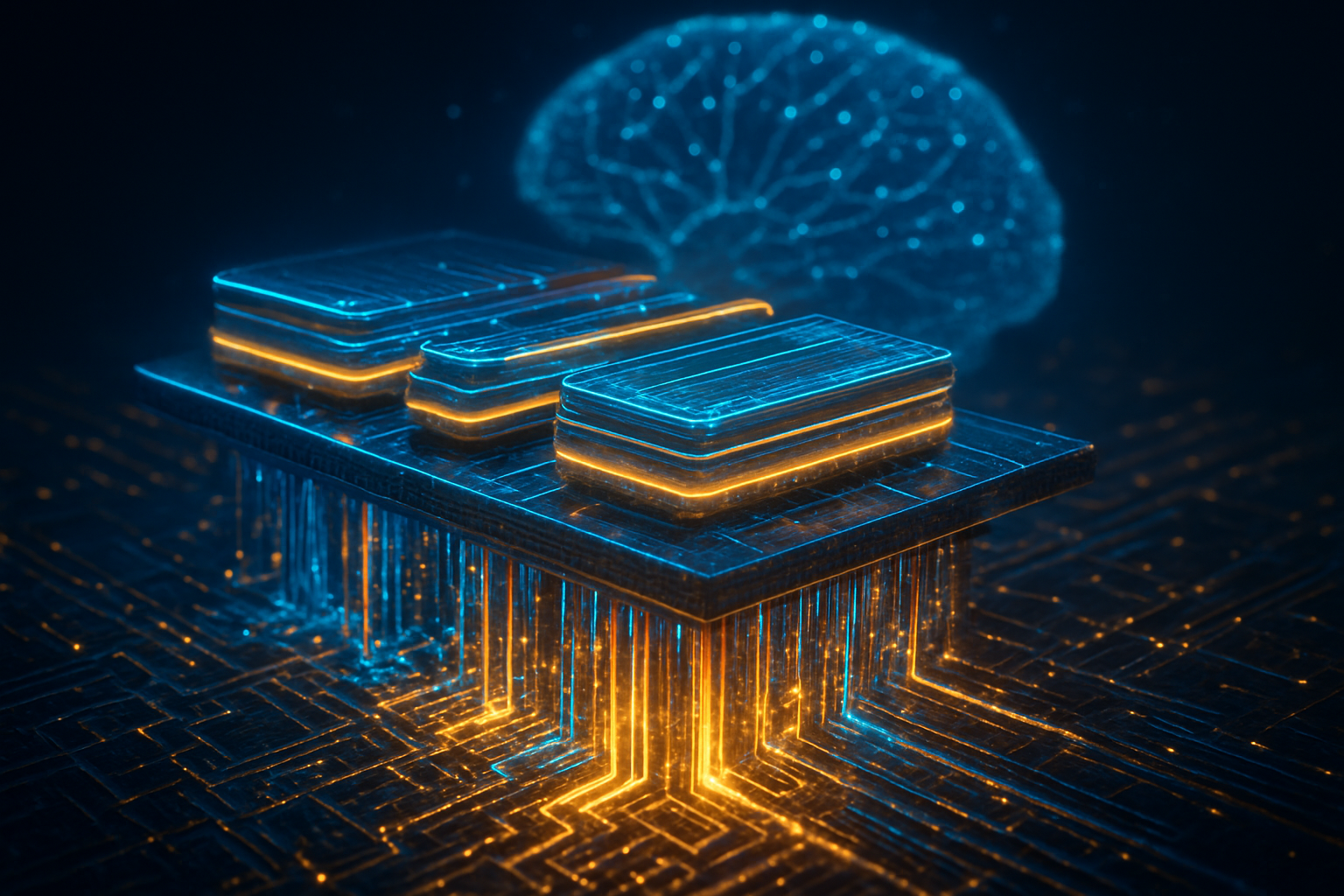
The significance of this release cannot be overstated. While 2024 and 2025 were characterized by experimental AI features and "beta" tags, the early 2026 update—internally codenamed "Luck E"—represents a stabilized, privacy-first AI platform that operates almost entirely on-device. With a focus on seamless communication and deep semantic understanding, Apple is attempting to solidify its lead in the "Edge AI" market, challenging the cloud-centric models of its primary rivals.
The Technical Core: On-Device Intelligence and Semantic Mastery
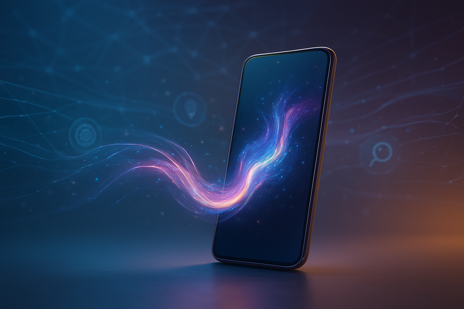
The centerpiece of the iOS 26 rollout is the introduction of Live Translation for calls, a feature that the industry has anticipated since the first Neural Engines were introduced. Unlike previous translation tools that required third-party apps or cloud processing, iOS 26 provides two-way, real-time spoken translation directly within the native Phone app. Utilizing a specialized version of Apple’s Large Language Models (LLMs) optimized for the A19 and A20 chips, the system translates the user’s voice into the recipient’s language and vice-versa, with a latency of less than 200 milliseconds. This "Real-Time Interpreter" also extends to FaceTime, providing live, translated captions that appear as an overlay during video calls.
Beyond verbal communication, Apple has overhauled the Messages app with AI-powered semantic search. Moving past simple keyword matching, the new search engine understands intent and context. A user can now ask, "Where did Sarah say she wanted to go for lunch next Tuesday?" and the system will cross-reference message history, calendar availability, and even shared links to provide a direct answer. This is powered by a local index that maps "personal context" without ever sending the data to a central server, a technical feat that Apple claims is unique to its hardware-software integration.
The creative suite has also seen a dramatic upgrade. Image Playground has shed its earlier "cartoonish" aesthetic for a more sophisticated, photorealistic engine. Users can now generate images in advanced artistic styles—including high-fidelity oil paintings and hyper-realistic digital renders—leveraging a deeper partnership with OpenAI for certain cloud-based creative tasks. Furthermore, Genmoji has evolved to include "Emoji Mixing," allowing users to merge existing Unicode emojis or create custom avatars from their Photos library that mirror specific facial expressions and hairstyles with uncanny accuracy.
The Competitive Landscape: The Battle for the AI Edge
The rollout of iOS 26 has sent ripples through the valuation of the world’s largest tech companies. As of early January 2026, Apple remains in a fierce battle with Alphabet (NASDAQ: GOOGL) and Nvidia (NASDAQ: NVDA) for market dominance. By prioritizing "Edge AI"—processing data on the device rather than the cloud—Apple has successfully differentiated itself from Google’s Gemini and Microsoft’s (NASDAQ: MSFT) Copilot, which still rely heavily on data center throughput.
This strategic pivot has significant implications for the broader industry:
- Hardware as a Moat: The advanced features of iOS 26 require the massive NPU (Neural Processing Unit) overhead found in the iPhone 17 and iPhone 15 Pro or later. This is expected to trigger what analysts call the "Siri Surge," a massive upgrade cycle as users on older hardware are left behind by the AI revolution.
- Disruption of Translation Services: Dedicated translation hardware and standalone apps are facing an existential threat as Apple integrates high-quality, offline translation into the core of the operating system.
- New Revenue Models: Apple has used this rollout to scale Apple Intelligence Pro, a $9.99 monthly subscription that offers priority access to Private Cloud Compute for complex tasks and high-volume image generation. This move signals a shift from a hardware-only revenue model to an "AI-as-a-Service" ecosystem.
Privacy, Ethics, and the Broader AI Landscape
As Apple Intelligence becomes more deeply woven into the fabric of daily life, the broader AI landscape is shifting toward "Personal Context Awareness." Apple’s approach stands in contrast to the "World Knowledge" models of 2024. While competitors focused on knowing everything about the internet, Apple has focused on knowing everything about you—while keeping that knowledge locked in a "black box" of on-device security.
However, this level of integration is not without concerns. Privacy advocates have raised questions about "On-Screen Awareness," a feature where Siri can "see" what is on a user's screen to provide context-aware help. Although Apple utilizes Private Cloud Compute (PCC)—a breakthrough in verifiable server-side security—to handle tasks that exceed on-device capabilities, the psychological barrier of an "all-seeing" AI remains a hurdle for mainstream adoption.
Comparatively, this milestone is being viewed as the "iPhone 4 moment" for AI. Just as the iPhone 4 solidified the smartphone as an essential tool for the modern era, iOS 26 is seen as the moment generative AI transitioned from a novelty into an invisible, essential utility.
The Horizon: From Personal Assistants to Autonomous Agents
Looking ahead, the early 2026 rollout is merely the foundation for Apple's long-term "Agentic" roadmap. Experts predict that the next phase will involve "cross-app autonomy," where Siri will not only find information but execute multi-step tasks—such as booking a flight, reserving a hotel, and notifying family members—all from a single prompt.
The challenges remain significant. Scaling these models to work across the entire ecosystem, including the Apple Watch and Vision Pro, requires further breakthroughs in power efficiency and model compression. Furthermore, as AI begins to handle more personal communications, the industry must grapple with the potential for "AI hallucination" in critical contexts like legal or medical translations.
A New Chapter in the Silicon Valley Narrative
The launch of iOS 26 and the expanded Apple Intelligence suite marks a definitive turning point in the AI arms race. By successfully integrating live translation, semantic search, and advanced generative tools into a privacy-first framework, Apple has proven that the future of AI may not live in massive, energy-hungry data centers, but in the pockets of billions of users.
The key takeaways from this rollout are clear: AI is no longer a standalone product; it is a layer of the operating system. As we move through the first quarter of 2026, the tech world will be watching closely to see how consumers respond to the "Apple Intelligence Pro" subscription and whether the "Siri Surge" translates into the record-breaking hardware sales that investors are banking on. For now, the iPhone has officially become more than a phone—it is a sentient, or at least highly intelligent, digital companion.
This content is intended for informational purposes only and represents analysis of current AI developments.
TokenRing AI delivers enterprise-grade solutions for multi-agent AI workflow orchestration, AI-powered development tools, and seamless remote collaboration platforms.
For more information, visit https://www.tokenring.ai/.