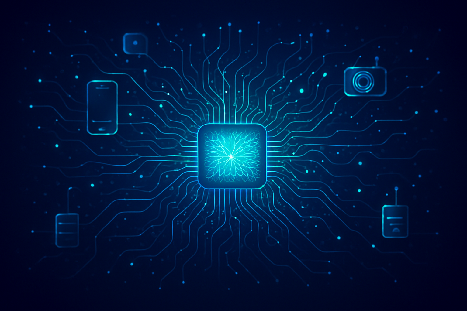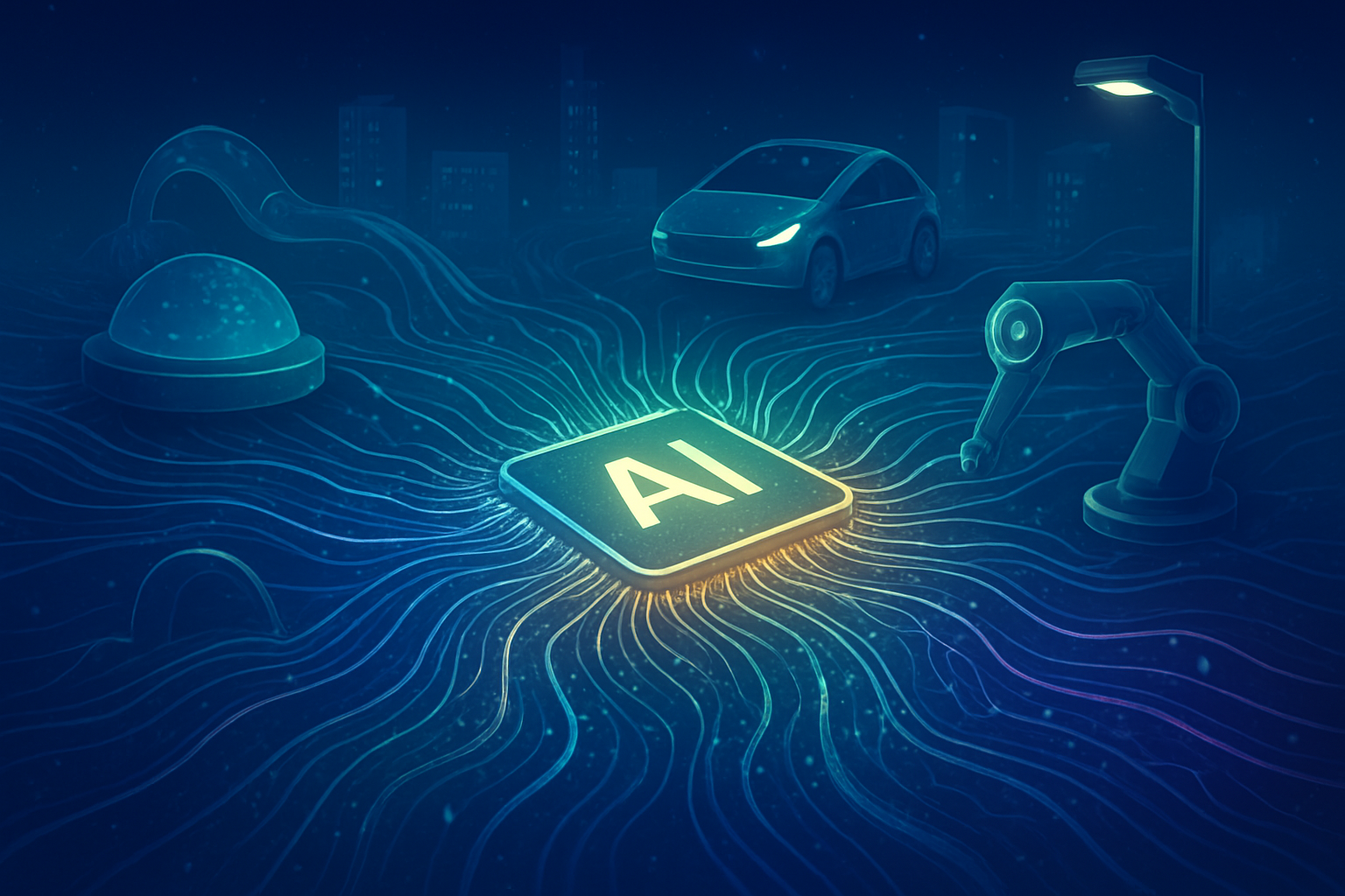
In a significant paradigm shift, Artificial Intelligence is moving out of the centralized cloud and into the devices that generate data, thanks to the rapid advancement of Edge AI processors. These specialized computing units are designed to execute AI algorithms and models directly on local "edge" devices—from smartphones and cameras to industrial machinery and autonomous vehicles. This decentralization of intelligence is not merely an incremental upgrade but a fundamental transformation, promising to unlock unprecedented levels of real-time responsiveness, data privacy, and operational efficiency across virtually every industry.
The immediate significance of Edge AI lies in its ability to process data at its source, dramatically reducing latency and enabling instantaneous decision-making critical for mission-critical applications. By minimizing data transmission to distant cloud servers, Edge AI also bolsters data privacy and security, reduces bandwidth requirements and associated costs, and enhances system reliability even in environments with intermittent connectivity. This evolution marks a pivotal moment, addressing the limitations of purely cloud-dependent AI and paving the way for a truly ubiquitous and intelligent ecosystem.
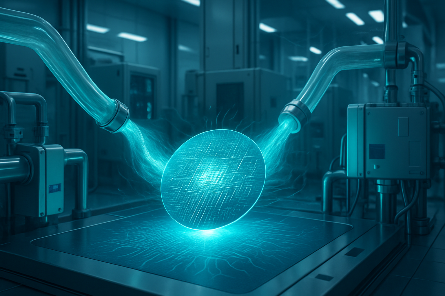
Technical Prowess: The Engine Behind On-Device Intelligence
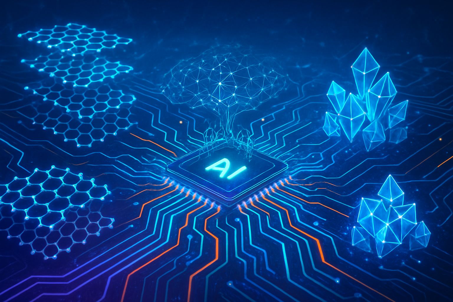
Edge AI processors are characterized by their specialized architectures, meticulously engineered for efficiency and performance within strict power and thermal constraints. At their core are dedicated AI accelerators, including Neural Processing Units (NPUs), Graphics Processing Units (GPUs), Digital Signal Processors (DSPs), Field-Programmable Gate Arrays (FPGAs), and Application-Specific Integrated Circuits (ASICs). NPUs, for instance, are purpose-built for neural network computations, accelerating tasks like matrix multiplication and convolution operations with high energy efficiency, offering more AI operations per watt than traditional CPUs or general-purpose GPUs. Companies like Intel (NASDAQ: INTC) with its AI Boost and AMD (NASDAQ: AMD) with its XDNA are integrating these units directly into their mainstream processors, while specialized players like Google (NASDAQ: GOOGL) with its Coral TPU and EdgeCortix with its SAKURA-I chips offer highly optimized ASICs for specific inference tasks.
These processors leverage significant advancements in AI model optimization, such as quantization (reducing numerical precision) and pruning (removing redundant nodes), which dramatically shrink the memory footprint and computational overhead of complex neural networks like MobileNet or TinyML models. This allows sophisticated AI to run effectively on resource-constrained devices, often operating within strict Thermal Design Power (TDP) limits, typically between 1W and 75W, far less than data center GPUs. Power efficiency is paramount, with metrics like TOPS/Watt (Tera Operations Per Second per Watt) becoming a key differentiator. The architectural trend is towards heterogeneous computing environments, combining various processor types within a single chip to optimize for performance, power, and cost, ensuring responsiveness for time-sensitive applications while maintaining flexibility for updates.
The fundamental difference from traditional cloud-based AI lies in the processing location. Cloud AI relies on remote, centralized data centers, incurring latency and requiring extensive data transmission. Edge AI processes data locally, eliminating these bottlenecks and enabling real-time decision-making crucial for applications like autonomous vehicles, where milliseconds matter. This localized processing also inherently enhances data privacy by minimizing the transmission of sensitive information to third-party cloud services and ensures offline capability, making devices resilient to network outages. While cloud AI still offers immense computational power for training large, complex models, Edge AI excels at efficient, low-latency inference, bringing AI's practical benefits directly to the point of action. The AI research community and industry experts widely acknowledge Edge AI as an "operational necessity," particularly for mission-critical applications, though they also point to challenges in resource constraints, development tools, and power management.
A New Battleground: Corporate Impact and Market Dynamics
The rise of Edge AI processors is creating a dynamic and intensely competitive landscape, reshaping strategic priorities for tech giants and opening new avenues for startups. Companies providing the foundational silicon stand to benefit immensely. NVIDIA (NASDAQ: NVDA), a leader in cloud AI GPUs, is aggressively expanding its edge presence with platforms like Jetson for robotics and embedded AI, and investing in AI-RAN products for next-generation networks. Intel (NASDAQ: INTC) is making a strong push with its Core Ultra processors and Tiber Edge Platform, aiming to integrate AI processing with high-performance computing at the edge, while AMD (NASDAQ: AMD) is also intensifying its efforts in AI computing with competitive GPUs and processors.
Qualcomm (NASDAQ: QCOM), a powerhouse in mobile, IoT, and automotive, is exceptionally well-positioned in the Edge AI semiconductor market. Its Snapdragon processors provide AI acceleration across numerous devices, and its Edge AI Box solutions target smart cities and factories, leveraging its mobile DNA for power-efficient, cost-effective inference at scale. Google (NASDAQ: GOOGL), through its custom Edge TPU and ML Kit platform, is optimizing its AI for on-device processing, as are other hyperscalers developing custom silicon to reduce dependency and optimize performance. Apple (NASDAQ: AAPL), with its Neural Engine Unit and Core ML, has been a pioneer in on-device AI for its vast ecosystem. Beyond these giants, companies like Samsung (KRX: 005930), MediaTek (TPE: 2454), and Arm Holdings (NASDAQ: ARM) are crucial players, alongside specialized startups like Hailo, Mythic, and Ambarella (NASDAQ: AMBA), which are developing ultra-efficient AI silicon tailored for specific edge applications.
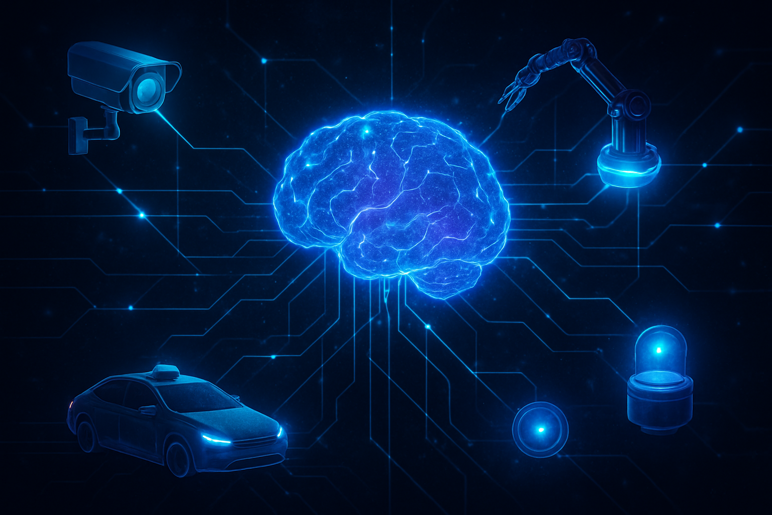
Edge AI is poised to disrupt numerous sectors by shifting from a cloud-centric "data transmission -> decision -> command" model to "on-site perception -> real-time decision -> intelligent service." This will fundamentally restructure device forms, business models, and value distribution in areas like AIoT, autonomous driving, and industrial automation. For instance, in healthcare, Edge AI enables real-time patient monitoring and diagnostics on wearables, protecting sensitive data locally. In manufacturing, it facilitates predictive maintenance and quality control directly on the factory floor. This decentralization also impacts business models, potentially shifting profitability towards "smart service subscriptions" that offer continuous, scenario-defined intelligent services. Strategic advantages are being forged through specialized hardware development, robust software ecosystems (like NVIDIA's CUDA or Intel's OpenVINO), vertical integration, strategic partnerships, and a strong focus on energy efficiency and privacy-centric AI.
Wider Significance: A New Era of Ubiquitous Intelligence
The wider significance of Edge AI processors cannot be overstated; they represent a crucial evolutionary step in the broader AI landscape. While cloud AI was instrumental in the initial training of complex models and generative AI, Edge AI addresses its inherent limitations, fostering a hybrid landscape where cloud AI handles large-scale training and analytics, and edge AI manages real-time inference and immediate actions. This decentralization of AI is akin to the shift from mainframe to client-server computing or the rise of cloud computing itself, bringing intelligence closer to the end-user and data source.
The impacts are far-reaching. On data privacy, Edge AI offers a robust solution by processing sensitive information locally, minimizing its exposure during network transmission and simplifying compliance with regulations like GDPR. Techniques such as federated learning allow collaborative model training without sharing raw data, further enhancing privacy. From a sustainability perspective, Edge AI contributes to a "Green AI" approach by reducing the energy consumption associated with transmitting and processing vast amounts of data in energy-intensive cloud data centers, lowering bandwidth usage and greenhouse gas emissions. It also enables energy optimization in smart factories, homes, and medical devices. Furthermore, Edge AI is a catalyst for new business models, enabling cost reduction through optimized infrastructure, real-time insights for ultra-fast decision-making (e.g., instant fraud detection), and new service-based models that offer personalized, intelligent services.
However, Edge AI also introduces potential concerns. Security is a primary challenge, as decentralized edge devices are often physically accessible and resource-constrained, making them vulnerable to tampering, unauthorized access, and adversarial attacks. Robust encryption, secure boot processes, and tamper-detection mechanisms are essential. Complexity is another hurdle; deploying sophisticated AI models on devices with limited computational power, memory, and battery life requires aggressive optimization, which can sometimes degrade accuracy. Managing and updating models across thousands of geographically dispersed devices, coupled with the lack of standardized tools and diverse hardware capabilities, adds significant layers of complexity to development and deployment. Despite these challenges, Edge AI marks a pivotal moment, transitioning AI from a predominantly centralized paradigm to a more distributed, ubiquitous, and real-time intelligent ecosystem.
The Horizon: Future Developments and Expert Predictions
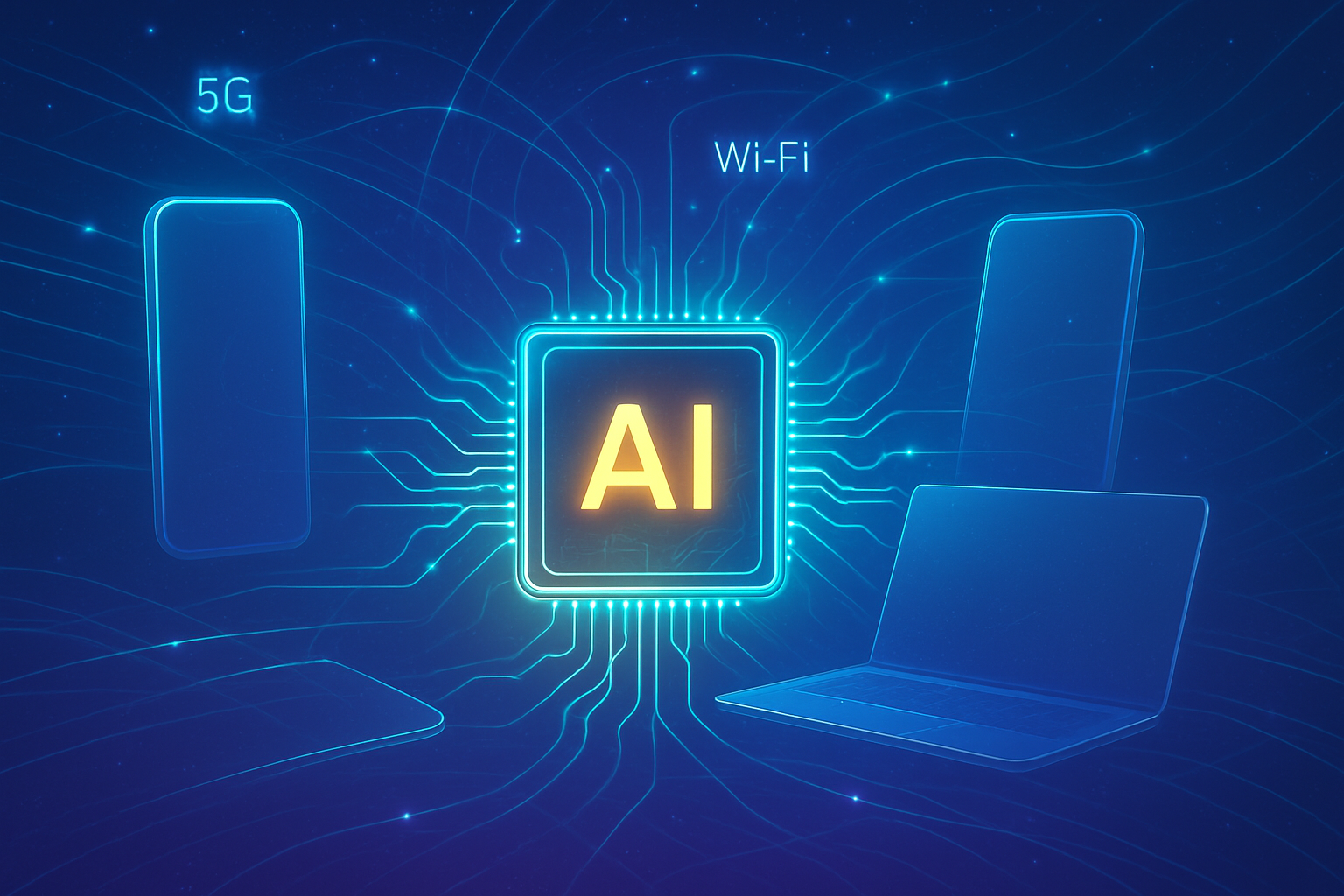
The future of Edge AI processors promises continuous innovation, driven by the insatiable demand for more powerful, efficient, and autonomous AI. In the near term (1-3 years), expect to see a relentless focus on increasing performance and energy efficiency, with chips capable of hundreds of TOPS at low power consumption. Specialized architectures—more powerful TPUs, NPUs, and ASICs—will continue to evolve, tailored for specific AI workloads. The widespread rollout of 5G networks will further accelerate Edge AI capabilities, providing the necessary high-speed, low-latency connectivity for large-scale, real-time deployments. Compute density and miniaturization will remain key, enabling complex AI models to run on even smaller, more resource-constrained devices, often integrated into hybrid edge-to-cloud processing systems.
Looking to the long term (3+ years and beyond), the landscape becomes even more revolutionary. Neuromorphic computing, with its brain-inspired architectures that integrate memory and processing, is poised to offer unparalleled energy efficiency and real-time learning capabilities directly at the edge. This will enable continuous adaptation and intelligence in autonomous systems, robotics, and decentralized medical AI. The integration of neuromorphic AI with future 6G networks and even quantum computing holds the promise of ultra-low-latency, massively parallel processing at the edge. Federated learning will become increasingly dominant, allowing AI systems to learn dynamically across vast networks of devices without centralizing sensitive data. Advanced chip architectures like RISC-V processors optimized for AI inference, in-memory compute, and 3D chip stacking will push the boundaries of performance and power delivery.
These advancements will unlock a myriad of new applications: truly autonomous vehicles making instant decisions, intelligent robots performing complex tasks independently, smart cities optimizing traffic and public safety in real-time, and pervasive AI in healthcare for remote diagnostics and personalized monitoring. However, challenges remain. Hardware limitations, power consumption, scalability, security, and the complexity of model optimization and deployment across diverse devices are critical hurdles. Experts predict that Edge AI will become the primary driver of real-time, autonomous intelligence, with hybrid AI architectures combining cloud training with edge inference becoming the norm. The global market for Edge AI chips is forecast for significant growth, with consumer electronics, industrial, and automotive sectors leading the charge, as major tech companies and governments heavily invest in this transformative technology.
The Dawn of Distributed Intelligence: A Concluding Perspective
The journey of Edge AI processors from a niche concept to a mainstream technological imperative marks a profound moment in AI history. We are witnessing a fundamental shift from centralized, cloud-dependent intelligence to a more distributed, ubiquitous, and real-time intelligent ecosystem. The key takeaways underscore its ability to deliver unparalleled speed, enhanced privacy, reduced costs, and improved reliability, making AI practical and pervasive across an ever-expanding array of real-world applications.
This development is not merely an incremental improvement; it is a strategic evolution that addresses the inherent limitations of purely cloud-based AI, particularly in an era dominated by the exponential growth of IoT devices and the demand for instantaneous, secure decision-making. Its long-term impact promises to be transformative, revolutionizing industries from healthcare and automotive to manufacturing and smart cities, while enhancing data privacy and fostering new economic models driven by intelligent services.
In the coming weeks and months, watch closely for new hardware releases from industry giants like NVIDIA (NASDAQ: NVDA), AMD (NASDAQ: AMD), Intel (NASDAQ: INTC), and Qualcomm (NASDAQ: QCOM), as well as innovative startups. Pay attention to the maturation of software ecosystems, open-source frameworks, and the seamless integration of 5G connectivity. Emerging trends like "thick edge" training, micro and thin edge intelligence, TinyML, federated learning, and neuromorphic computing will define the next wave of innovation. Edge AI is not just a technological trend; it is the dawn of distributed intelligence, promising a future where AI operates at the source, powering industries, cities, and everyday life with unprecedented efficiency and autonomy.
This content is intended for informational purposes only and represents analysis of current AI developments.
TokenRing AI delivers enterprise-grade solutions for multi-agent AI workflow orchestration, AI-powered development tools, and seamless remote collaboration platforms.
For more information, visit https://www.tokenring.ai/.