Tag: AI Silicon

  • The Bespoke Billion: How Broadcom Is Architecting the Post-Nvidia AI Era Through Custom Silicon and Light

    The Bespoke Billion: How Broadcom Is Architecting the Post-Nvidia AI Era Through Custom Silicon and Light

    As of February 6, 2026, the artificial intelligence landscape is witnessing a monumental shift in power. While the initial wave of the AI revolution was defined by general-purpose GPUs, the current era belongs to "bespoke compute." Broadcom Inc. (NASDAQ: AVGO) has emerged as the primary architect of this new world, solidifying its leadership in custom AI Application-Specific Integrated Circuits (ASICs) and revolutionary silicon photonics. Analysts across Wall Street have responded with a wave of "Overweight" ratings, signaling that Broadcom’s role as the indispensable backbone of the hyperscale data center is no longer a projection—it is a reality.

    The significance of Broadcom’s ascent lies in its ability to help the world’s largest tech companies bypass the high costs and supply constraints of general-purpose chips. By delivering specialized accelerators (XPUs) tailored to specific AI models, Broadcom is enabling a transition toward more efficient, cost-effective, and scalable infrastructure. With AI-related revenue projected to reach nearly $50 billion this year, the company is no longer just a networking player; it is the central engine for the custom-built AI future.

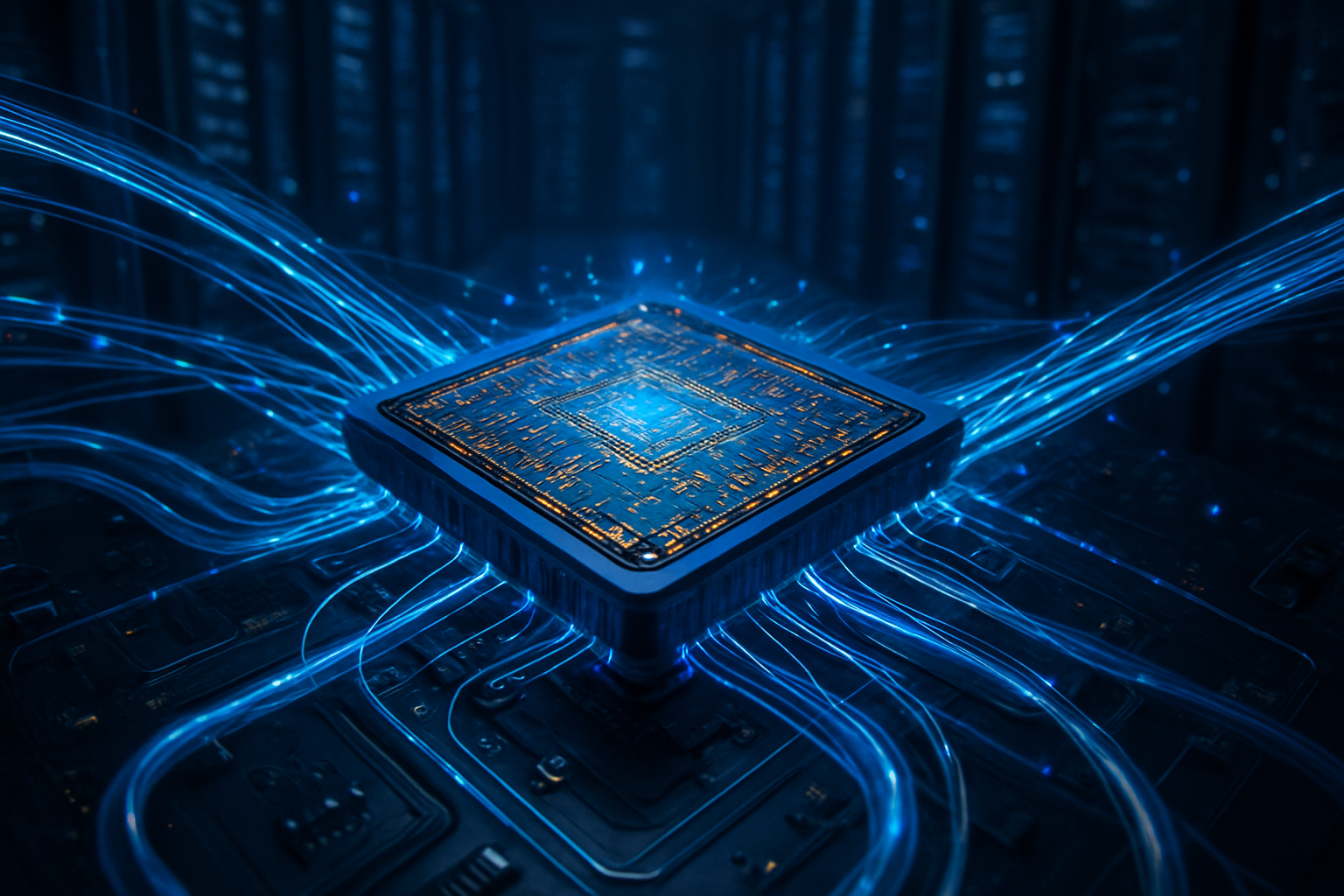
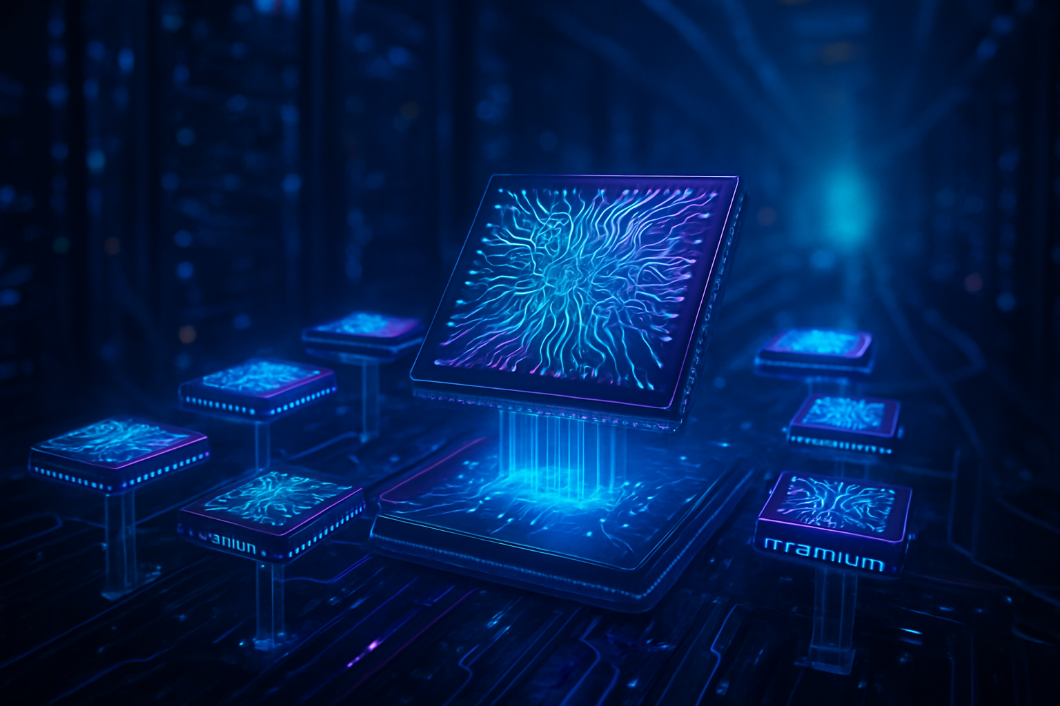
    At the heart of Broadcom’s technical dominance is the shipping of the Tomahawk 6 series, the world’s first 102.4 Terabits per second (Tbps) switching silicon. Announced in late 2025 and seeing massive volume deployment in early 2026, the Tomahawk 6 doubles the bandwidth of its predecessor, facilitating the interconnection of million-node XPU clusters. Unlike previous generations, the Tomahawk 6 is built specifically for the "Scale-Out" requirements of Generative AI, utilizing 200G SerDes (Serializer/Deserializer) technology to handle the unprecedented data throughput required for training trillion-parameter models.

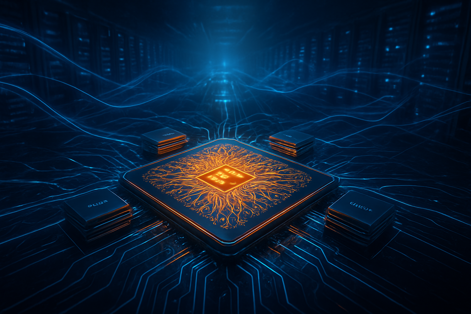
    Broadcom is also pioneering the use of Co-Packaged Optics (CPO) through its "Davisson" platform. In traditional data centers, electrical signals are converted to light using pluggable transceivers at the edge of the switch. Broadcom’s CPO technology integrates the optical engines directly onto the ASIC package, reducing power consumption by 3.5x and lowering the cost per bit by 40%. This breakthrough addresses the "power wall"—the physical limit of how much electricity a data center can consume—by eliminating energy-intensive copper components. Furthermore, the newly released Jericho 4 router chip introduces "Cognitive Routing," a feature that uses hardware-level intelligence to manage congestion and prevent "packet stalls," which can otherwise derail multi-week AI training jobs.

    This technological leap has major implications for tech giants like Google (NASDAQ: GOOGL), Meta (NASDAQ: META), and OpenAI. Analysts from firms like Wells Fargo and Bank of America note that Broadcom is the primary beneficiary of the "Nvidia tax" avoidance strategy. Hyperscalers are increasingly moving away from Nvidia (NASDAQ: NVDA) proprietary stacks in favor of custom XPUs. For instance, Broadcom is the lead partner for Google’s TPU v7 and Meta’s MTIA v4. These custom chips are optimized for the companies' specific workloads—such as Llama-4 or Gemini—offering performance-per-watt metrics that general-purpose GPUs cannot match.

    The market positioning is further bolstered by a landmark partnership with OpenAI. Broadcom is reportedly providing the silicon architecture for OpenAI’s massive 10-gigawatt data center initiative, an endeavor estimated to have a lifetime value exceeding $100 billion. By providing a vertically integrated solution that includes the compute ASIC, the high-speed Ethernet NIC (Thor Ultra), and the back-end switching fabric, Broadcom offers a "turnkey" custom silicon service. This puts pressure on traditional chipmakers and provides a strategic advantage to AI labs that want to control their own hardware destiny without the overhead of building an entire chip division from scratch.

    Broadcom’s success reflects a broader trend in the AI industry: the triumph of open standards over proprietary ecosystems. While Nvidia’s InfiniBand was once the gold standard for AI networking, the industry has shifted back toward Ethernet, largely due to Broadcom’s innovations. The Ultra Ethernet Consortium (UEC), of which Broadcom is a founding member, has standardized the protocols that allow Ethernet to match or exceed InfiniBand’s latency and reliability. This shift ensures that the AI infrastructure of the future remains interoperable, preventing any single vendor from maintaining a permanent monopoly on the data center fabric.

    However, this transition is not without concerns. The extreme concentration of Broadcom’s revenue among a handful of hyperscale customers—Google, Meta, and OpenAI—creates a dependency that analysts watch closely. Furthermore, as AI models become more specialized, the "bespoke" nature of these chips means they lack the versatility of GPUs. If the industry were to pivot toward a fundamentally different neural architecture, custom ASICs could face faster obsolescence. Despite these risks, the current trajectory suggests that the efficiency gains of custom silicon are too significant for the world's largest compute spenders to ignore.

    Looking ahead to the remainder of 2026 and into 2027, Broadcom is already laying the groundwork for Gen 4 Co-Packaged Optics. This next generation aims to achieve 400G per lane capability, effectively doubling networking speeds again within the next 24 months. Experts predict that as the industry moves toward 200-terabit switches, the integration of silicon photonics will move from a competitive advantage to a mandatory requirement. We also expect to see "edge-to-cloud" custom silicon initiatives, where Broadcom-designed chips power both the massive training clusters in the cloud and the localized inference engines in high-end consumer devices.

    The next major milestone to watch will be the full-scale deployment of "optical interconnects" between individual XPUs, effectively turning a whole data center rack into a single, giant, light-speed computer. While challenges remain in the yield and manufacturing complexity of these advanced packages, Broadcom’s partnership with leading foundries suggests they are on track to overcome these hurdles. The goal is clear: to reach a point where networking and compute are indistinguishable, linked by a seamless fabric of silicon and light.

    In summary, Broadcom has successfully transformed itself from a diversified component supplier into the vital architect of the AI infrastructure era. By dominating the two most critical bottlenecks in AI—bespoke compute and high-speed networking—the company has secured a massive backlog of orders that analysts believe will drive $100 billion in AI revenue by 2027. The move to an "Overweight" rating by major financial institutions is a recognition that Broadcom’s silicon photonics and ASIC leadership provide a "moat" that is becoming increasingly difficult for competitors to cross.

    As we move further into 2026, the industry should watch for the first real-world performance benchmarks of the OpenAI custom clusters and the broader adoption of the Tomahawk 6. These milestones will likely confirm whether the shift toward custom, Ethernet-based AI fabrics is the permanent blueprint for the next decade of computing. For now, Broadcom stands as the quiet giant of the AI revolution, proving that in the race for artificial intelligence, the one who controls the flow of data—and the light that carries it—ultimately wins.


    This content is intended for informational purposes only and represents analysis of current AI developments.

    TokenRing AI delivers enterprise-grade solutions for multi-agent AI workflow orchestration, AI-powered development tools, and seamless remote collaboration platforms.
    For more information, visit https://www.tokenring.ai/.

  • The Bespoke Silicon Revolution: Broadcom’s $50 Billion Surge Redefines the AI Hardware Landscape

    The Bespoke Silicon Revolution: Broadcom’s $50 Billion Surge Redefines the AI Hardware Landscape

    As of early 2026, the artificial intelligence industry has reached a critical inflection point where generic hardware is no longer enough to satisfy the hunger of multi-trillion parameter models. Leading this fundamental shift is Broadcom Inc. (NASDAQ: AVGO), which has successfully transitioned from a diversified networking giant into the primary architect of the custom AI silicon era. By positioning itself as the indispensable partner for hyperscalers like Google and Meta, and now the primary engine behind OpenAI’s hardware ambitions, Broadcom is witnessing a historic surge in revenue that is reshaping the semiconductor market.

    The numbers tell a story of rapid, unprecedented dominance. After closing a blockbuster fiscal year 2025 with $20 billion in AI-related revenue, Broadcom is now on track to more than double that figure in 2026, with projections soaring toward the $50 billion mark. With an AI order backlog currently sitting at a staggering $73 billion, the company has effectively bifurcated the AI chip market: while Nvidia Corp. (NASDAQ: NVDA) remains the king of general-purpose training, Broadcom has become the undisputed sovereign of custom Application-Specific Integrated Circuits (ASICs), providing the "bespoke compute" that allows the world’s largest tech companies to bypass the "Nvidia tax" and build more efficient, specialized data centers.

    Engineering the Architecture of Sovereign AI

    The core of Broadcom’s technical advantage lies in its ability to co-design chips that strip away the silicon "cruft" found in general-purpose GPUs. While Nvidia’s Blackwell and newly released Rubin platforms must support a vast array of legacy applications and diverse workloads, Broadcom’s ASICs—such as Google’s (NASDAQ: GOOGL) TPU v7 and Meta Platforms' (NASDAQ: META) MTIA v4—are laser-focused on the specific mathematical operations required for Large Language Models (LLMs). This specialization allows for a 30% to 50% improvement in performance-per-watt compared to off-the-shelf GPUs. In an era where data center power limits have become the primary bottleneck for AI scaling, this energy efficiency is not just a cost-saving measure; it is a strategic necessity.

    The technical specifications of these new accelerators are formidable. The Google TPU v7 (codenamed "Ironwood"), built on a 3nm process, is optimized specifically for the latest Gemini 2.0 and 3.0 models. Meanwhile, the Meta MTIA v4 (Santa Barbara), currently deploying across Meta’s massive fleet of servers, features liquid-cooled rack integration and advanced 3D Torus networking topologies. This architecture allows companies to cluster over 9,000 chips into a single unified "Superpod" with minimal latency, far exceeding the scale of traditional GPU clusters. Broadcom provides the critical intellectual property—including high-speed SerDes, HBM controllers, and networking interconnects—while leveraging its deep partnership with Taiwan Semiconductor Manufacturing Co. (NYSE: TSM) for advanced packaging.

    Shifting the Competitive Power Balance

    This surge in custom silicon is fundamentally altering the power dynamics among tech giants. By developing their own chips through Broadcom, companies like Meta and Google are achieving a level of vertical integration that provides a significant competitive moat. For these hyperscalers, the shift to ASICs represents a "decoupling" from the supply chain volatility and high margins associated with third-party GPU vendors. It allows them to optimize their entire stack—from the underlying silicon and networking to the AI models themselves—resulting in a lower Total Cost of Ownership (TCO) that startups and smaller labs simply cannot match.

    The market is also witnessing the emergence of a "second tier" of custom silicon providers, most notably Marvell Technology Inc. (NASDAQ: MRVL), which has secured its own landmark deals with Amazon and Microsoft. However, Broadcom remains the dominant force, controlling roughly 65% of the custom AI ASIC market. This positioning has made Broadcom a "proxy" for the overall health of the AI infrastructure sector. As OpenAI officially joins Broadcom’s customer roster with a multi-billion dollar project to build its own "sovereignty" chip, the company’s role has evolved from a supplier to a strategic kingmaker. OpenAI’s move to internal silicon, specifically designed to run its high-intensity "reasoning" models like the o1-series, signals that the industry's heaviest hitters are no longer content with being customers—they want to be architects.

    The Broader Implications for the AI Landscape

    Broadcom’s success reflects a broader trend toward the fragmentation of the AI hardware landscape. We are moving away from a world of "one size fits all" compute and toward a heterogeneous environment where different chips are tuned for specific tasks: training, inference, or reasoning. This shift mimics the evolution of the mobile industry, where Apple’s move to internal silicon eventually redefined the performance benchmarks for the entire smartphone market. By enabling Google, Meta, and OpenAI to do the same for AI, Broadcom is accelerating a future where the most advanced AI capabilities are tied directly to proprietary hardware.

    However, this trend toward custom silicon also raises concerns about market consolidation. As the barrier to entry for high-end AI moves from "buying GPUs" to "designing multi-billion dollar custom chips," the gap between the "Big Five" hyperscalers and the rest of the industry may become an unbridgeable chasm. Furthermore, the reliance on a few key players—specifically Broadcom for design and TSMC for fabrication—creates new points of failure in the global AI supply chain. The environmental impact is also a double-edged sword; while ASICs are more efficient per operation, the sheer scale of the new data centers being built to house them is driving global energy demand to unprecedented heights.

    The Horizon: 2nm Nodes and Reasoning-Specific Silicon

    Looking toward 2027 and beyond, the roadmap for custom silicon is focused on the transition to 2nm-class nodes and the integration of even more advanced "Chip-on-Wafer-on-Substrate" (CoWoS) packaging. Broadcom is already in the early stages of development for the TPU v8, which is expected to begin mass production in the second half of 2026. These next-generation chips will likely incorporate on-chip optical interconnects, further reducing the latency and energy costs associated with moving data between processors and memory—a critical requirement for the next generation of "Agentic AI" that must process information in real-time.

    Experts predict that the next major frontier will be the development of silicon specifically optimized for "reasoning-heavy" inference. Current chips are largely designed for the "next-token prediction" paradigm of GPT-4. However, as models move toward more complex chain-of-thought processing, the demand for chips with significantly higher local memory bandwidth and specialized logic for logic-gate simulation will grow. Broadcom’s partnership with OpenAI is widely believed to be the first major step in this direction, potentially creating a new category of "Reasoning Units" that differ fundamentally from current NPUs and GPUs.

    Conclusion: A Legacy Defined by Customization

    Broadcom’s transformation into an AI silicon powerhouse is one of the most significant developments in the history of the semiconductor industry. By 2026, the company has proven that the path to AI supremacy is paved with customization, not just raw power. Its $50 billion revenue surge is a testament to the fact that for the world’s most advanced AI labs, the "off-the-shelf" era is effectively over. Broadcom’s ability to turn the complex requirements of companies like Google, Meta, and OpenAI into physical, high-performance silicon has placed it at the center of the AI ecosystem.

    In the coming months, the industry will be watching closely as the first "live silicon" from the OpenAI-Broadcom partnership begins to ship. This event will likely serve as a litmus test for whether internal silicon can truly provide the "sovereignty" that AI labs crave. For investors and technologists alike, Broadcom is no longer just a networking company; it is the master builder of the infrastructure that will define the next decade of artificial intelligence.


    This content is intended for informational purposes only and represents analysis of current AI developments.

    TokenRing AI delivers enterprise-grade solutions for multi-agent AI workflow orchestration, AI-powered development tools, and seamless remote collaboration platforms.
    For more information, visit https://www.tokenring.ai/.

  • Broadcom’s Custom AI Silicon Boom: Beyond the Google TPU

    Broadcom’s Custom AI Silicon Boom: Beyond the Google TPU

    As of early 2026, the artificial intelligence landscape is witnessing a seismic shift in how the world’s most powerful models are powered. While the industry spent years in the shadow of general-purpose GPUs, a new era of "bespoke compute" has arrived, spearheaded by Broadcom Inc. (NASDAQ: AVGO). Once synonymous primarily with Google’s (NASDAQ: GOOGL) Tensor Processing Units (TPUs), Broadcom has successfully diversified its custom AI Application-Specific Integrated Circuit (ASIC) business into a multi-customer powerhouse, securing landmark deals with Meta (NASDAQ: META), OpenAI, and Anthropic.

    This transition marks a pivotal moment in the "Compute Wars." By co-designing specialized silicon and high-speed networking fabrics, Broadcom is enabling hyperscalers to break free from the supply constraints and high premiums associated with off-the-shelf hardware. With AI-related revenue projected to hit a staggering $46 billion in 2026—a 134% year-over-year increase—Broadcom has effectively positioned itself as the structural architect of the next generation of AI infrastructure.

    The Technical Edge: TPU v7, MTIA v4, and the 1.6T Networking Revolution

    The technical foundation of Broadcom’s dominance lies in its ability to integrate high-performance compute with industry-leading networking. In late 2025, Broadcom and Google debuted the TPU v7 (Ironwood), a 3nm marvel designed specifically for large-scale inference and reasoning. Featuring 192GB of HBM3e memory and a massive 9.6 Tbps Inter-Chip Interconnect (ICI) bandwidth, Ironwood is optimized for the multi-trillion parameter models that define the current AGI-frontier. Similarly, the partnership with Meta has moved into its next phase with the MTIA v4 (Santa Barbara), which introduces liquid-cooled rack integration to handle the unprecedented thermal demands of 180kW+ AI clusters.

    Perhaps most significant is Broadcom’s advancements in networking, which serve as the "connective tissue" for these custom chips. The Tomahawk 6 (TH6) switch ASIC, shipping in volume as of early 2026, is the world’s first 102.4 Tbps switch, enabling the transition to 1.6T Ethernet. This allows for the creation of clusters containing over one million XPUs (accelerated processing units) with minimal latency. By championing the Ethernet for Scale-Up Networking (ESUN) workstream, Broadcom is providing a viable, open-standard alternative to NVIDIA’s (NASDAQ: NVDA) proprietary NVLink, allowing customers to build "scale-up" fabrics within the rack using standard Ethernet protocols.

    Industry experts note that this "end-to-end" approach—where the AI chip and the network switch are co-designed—solves the "IO bottleneck" that has long plagued large-scale AI training. Initial reactions from the research community suggest that Broadcom’s custom silicon-plus-Ethernet strategy provides up to 50% better throughput for distributed training tasks compared to traditional InfiniBand-based setups.

    Reducing the "NVIDIA Tax" and Empowering the Hyperscale Elite

    The strategic implications of Broadcom’s custom silicon boom are profound. For years, the "NVIDIA tax"—the high margin paid for H100 and Blackwell GPUs—was the cost of doing business in AI. However, companies like Meta and Google have realized that at their scale, even a 10% efficiency gain in silicon can save billions in capital expenditure and energy costs. By partnering with Broadcom, these giants gain total control over the instruction set architecture (ISA), memory configurations, and power envelopes of their hardware, tailoring them specifically to their proprietary algorithms.

    The recent entry of OpenAI and Anthropic into Broadcom’s custom silicon stable has sent shockwaves through the industry. OpenAI’s landmark collaboration to co-develop custom accelerators for its 10-gigawatt data center projects signifies a long-term pivot toward hardware sovereignty. Anthropic, similarly, has committed to a $10 billion+ deal for custom silicon, aiming to optimize its Claude models on hardware that prioritizes safety-aligned "constitutional AI" features at the silicon level. This shift significantly dilutes NVIDIA’s market dominance, as the most valuable AI workloads move from general-purpose GPUs to specialized ASICs.

    For Broadcom, this diversification creates a "structural moat." Unlike competitors who may offer only the chip or only the switch, Broadcom’s portfolio includes the SerDes, the HBM controllers, the optical interconnects, and the networking silicon. This vertical integration makes them the indispensable partner for any company large enough to design its own chip but too small to manage the entire semiconductor manufacturing and networking stack alone.

    A New Global Standard: The Rise of Sovereign AI Compute

    Broadcom’s success fits into a broader trend of "Sovereign AI," where both corporations and nations seek to control their own compute destiny. The move toward custom ASICs is not just about cost; it is about performance ceilings. As LLMs evolve into "Large World Models" that incorporate video, audio, and real-time physical simulation, the data movement requirements are exceeding what general-purpose hardware can provide. Broadcom’s introduction of the Jericho4 ASIC, which enables Data Center Interconnects (DCI) across distances of up to 100km with lossless performance, is a direct response to the power and space constraints of single-site mega-datacenters.

    There are, however, concerns regarding the concentration of power. With Broadcom holding a nearly 60% market share in the custom AI ASIC space, the industry has effectively traded one gatekeeper (NVIDIA) for another. Furthermore, the reliance on high-end 3nm and 2nm manufacturing nodes at TSMC (NYSE: TSM) remains a potential geopolitical bottleneck. Despite these concerns, the shift to custom silicon is viewed as a necessary evolution for the industry to reach the next milestone in AI capability without collapsing the global energy grid.

    The Horizon: 2nm Processes and Co-Packaged Optics

    Looking ahead to 2027 and beyond, Broadcom is already laying the groundwork for the next jump in performance. The transition to 2nm process technology is expected to yield another 30% improvement in energy efficiency, a critical metric as AI power consumption becomes a global regulatory concern. Furthermore, the adoption of Co-Packaged Optics (CPO) will likely become the standard for 3.2T and 6.4T networking, replacing traditional copper and pluggable transceivers with silicon photonics integrated directly onto the chip package.

    Predictive models suggest that by late 2026, the majority of "Frontier Model" training will occur on custom ASICs rather than general-purpose GPUs. We may also see Broadcom expand its "silicon-as-a-service" model, potentially offering modular chiplet designs that allow smaller tech companies to "mix and match" Broadcom’s networking IP with their own proprietary logic.

    Conclusion: Broadcom's Indispensable Role in the AI Era

    Broadcom’s transformation from a diversified semiconductor firm into the primary architect of the world’s AI infrastructure is one of the most significant business stories of the mid-2020s. By moving "beyond the Google TPU" and securing the top tier of AI labs—Meta, OpenAI, and Anthropic—Broadcom has proven that the future of AI is bespoke. Its dual-threat mastery of both custom compute and high-speed Ethernet networking has created a feedback loop that will be difficult for any competitor, even NVIDIA, to break.

    As we move through 2026, the key developments to watch will be the first live silicon deployments from the OpenAI-Broadcom partnership and the industry-wide adoption of 1.6T Ethernet. Broadcom is no longer just a component supplier; it is the platform upon which the age of AGI is being built.


    This content is intended for informational purposes only and represents analysis of current AI developments.

    TokenRing AI delivers enterprise-grade solutions for multi-agent AI workflow orchestration, AI-powered development tools, and seamless remote collaboration platforms.
    For more information, visit https://www.tokenring.ai/.

  • The Custom Silicon Gold Rush: How Broadcom and the ‘Cloud Titans’ are Challenging Nvidia’s AI Dominance

    The Custom Silicon Gold Rush: How Broadcom and the ‘Cloud Titans’ are Challenging Nvidia’s AI Dominance

    As of January 22, 2026, the artificial intelligence industry has reached a pivotal inflection point, shifting from a mad scramble for general-purpose hardware to a sophisticated era of architectural vertical integration. Broadcom (NASDAQ: AVGO), long the silent architect of the internet’s backbone, has emerged as the primary beneficiary of this transition. In its latest fiscal report, the company revealed a staggering $73 billion AI-specific order backlog, signaling that the world’s largest tech companies—Google (NASDAQ: GOOGL), Meta (NASDAQ: META), and now OpenAI—are increasingly bypassing traditional GPU vendors in favor of custom-tailored silicon.

    This surge in custom "XPUs" (AI accelerators) marks a fundamental change in the economics of the cloud. By partnering with Broadcom to design application-specific integrated circuits (ASICs), the "Cloud Titans" are achieving performance-per-dollar metrics that were previously unthinkable. This development not only threatens the absolute dominance of the general-purpose GPU but also suggests that the next phase of the AI race will be won by those who own their entire hardware and software stack.

    Custom XPUs: The Technical Blueprint of the Million-Accelerator Era

    The technical centerpiece of this shift is the arrival of seventh and eighth-generation custom accelerators. Google’s TPU v7, codenamed "Ironwood," which entered mass deployment in late 2025, has set a new benchmark for efficiency. By optimizing the silicon specifically for Google’s internal software frameworks like JAX and XLA, Broadcom and Google have achieved a 70% reduction in cost-per-token compared to the previous generation. This leap puts custom silicon at parity with, and in some specific training workloads, ahead of Nvidia’s (NASDAQ: NVDA) Blackwell architecture.

    Beyond the compute cores themselves, Broadcom is solving the "interconnect bottleneck" that has historically limited AI scaling. The introduction of the Tomahawk 6 (Davisson) switch—the industry’s first 102.4 Terabits per second (Tbps) single-chip Ethernet switch—allows for the creation of "flat" network topologies. This enables hyperscalers to link up to one million XPUs in a single, cohesive fabric. In early 2026, this "Million-XPU" cluster capability has become the new standard for training the next generation of Frontier Models, which now require compute power measured in gigawatts rather than megawatts.

    A critical technical differentiator for Broadcom is its 3rd-generation Co-Packaged Optics (CPO) technology. As AI power demands reach nearly 200kW per server rack, traditional pluggable optical modules have become a primary source of heat and energy waste. Broadcom’s CPO integrates optical interconnects directly onto the chip package, reducing power consumption for data movement by 30-40%. This integration is essential for the 3nm and upcoming 2nm production nodes, where thermal management is as much of a constraint as transistor density.

    Industry experts note that this move toward ASICs represents a "de-generalization" of AI hardware. While Nvidia’s H100 and B200 series are designed to run any model for any customer, custom silicon like Meta’s MTIA (Meta Training and Inference Accelerator) is stripped of unnecessary components. This leaner design allows for more area on the die to be dedicated to high-bandwidth memory (HBM3e and HBM4) and specialized matrix-math units, specifically tuned for the recommendation algorithms and Large Language Models (LLMs) that drive Meta’s core business.

    Market Shift: The Rise of the ASIC Alliances

    The financial implications of this shift are profound. Broadcom’s AI-related semiconductor revenue hit $6.5 billion in the final quarter of 2025, a 74% year-over-year increase, with guidance for Q1 2026 suggesting a jump to $8.2 billion. This trajectory has repositioned Broadcom not just as a component supplier, but as a strategic peer to the world's most valuable companies. The company’s shift toward selling complete "AI server racks"—inclusive of custom silicon, high-speed switches, and integrated optics—has increased the total dollar value of its customer engagements ten-fold.

    Meta has particularly leaned into this strategy through its "Project Santa Barbara" rollout in early 2026. By doubling its in-house chip capacity using Broadcom-designed silicon, Meta is significantly reducing its "Nvidia tax"—the premium paid for general-purpose flexibility. For Meta and Google, every dollar saved on hardware procurement is a dollar that can be reinvested into data acquisition and model training. This vertical integration provides a massive strategic advantage, allowing these giants to offer AI services at lower price points than competitors who rely solely on off-the-shelf components.

    Nvidia, while still the undisputed leader in the broader enterprise and startup markets due to its dominant CUDA software ecosystem, is facing a narrowing "moat" at the very top of the market. The "Big 5" hyperscalers, which account for a massive portion of Nvidia's revenue, are bifurcating their fleets: using Nvidia for third-party cloud customers who require the flexibility of CUDA, while shifting their own massive internal workloads to custom Broadcom-assisted silicon. This trend is further evidenced by Amazon (NASDAQ: AMZN), which continues to iterate on its Trainium and Inferentia lines, and Microsoft (NASDAQ: MSFT), which is now deploying its Maia 200 series across its Azure Copilot services.

    Perhaps the most disruptive announcement of the current cycle is the tripartite alliance between Broadcom, OpenAI, and various infrastructure partners to develop "Titan," a custom AI accelerator designed to power a 10-gigawatt computing initiative. This move by OpenAI signals that even the premier AI research labs now view custom silicon as a prerequisite for achieving Artificial General Intelligence (AGI). By moving away from general-purpose hardware, OpenAI aims to gain direct control over the hardware-software interface, optimizing for the unique inference requirements of its most advanced models.

    The Broader AI Landscape: Verticalization as the New Standard

    The boom in custom silicon reflects a broader trend in the AI landscape: the transition from the "exploration phase" to the "optimization phase." In 2023 and 2024, the goal was simply to acquire as much compute as possible, regardless of cost. In 2026, the focus has shifted to efficiency, sustainability, and total cost of ownership (TCO). This move toward verticalization mirrors the historical evolution of the smartphone industry, where Apple’s move to its own A-series and M-series silicon allowed it to outpace competitors who relied on generic chips.

    However, this trend also raises concerns about market fragmentation. As each tech giant develops its own proprietary hardware and optimized software stack (such as Google’s XLA or Meta’s PyTorch-on-MTIA), the AI ecosystem could become increasingly siloed. For developers, this means that a model optimized for AWS’s Trainium may not perform identically on Google’s TPU or Microsoft’s Maia, potentially complicating the landscape for multi-cloud AI deployments.

    Despite these concerns, the environmental impact of custom silicon cannot be overlooked. General-purpose GPUs are, by definition, less efficient than specialized ASICs for specific tasks. By stripping away the "dark silicon" that isn't used for AI training and inference, and by utilizing Broadcom's co-packaged optics, the industry is finding a path toward scaling AI without a linear increase in carbon footprint. The "performance-per-watt" metric has replaced raw TFLOPS as the most critical KPI for data center operators in 2026.

    This milestone also highlights the critical role of the semiconductor supply chain. While Broadcom designs the architecture, the entire ecosystem remains dependent on TSMC’s advanced nodes. The fierce competition for 3nm and 2nm capacity has turned the semiconductor foundry into the ultimate geopolitical and economic chokepoint. Broadcom’s success is largely due to its ability to secure massive capacity at TSMC, effectively acting as an aggregator of demand for the world’s largest tech companies.

    Future Horizons: The 2nm Era and Beyond

    Looking ahead, the roadmap for custom silicon is increasingly ambitious. Broadcom has already secured significant capacity for the 2nm production node, with initial designs for "TPU v9" and "Titan 2" expected to tape out in late 2026. These next-generation chips will likely integrate even more advanced memory technologies, such as HBM4, and move toward "chiplet" architectures that allow for even greater customization and yield efficiency.

    In the near term, we expect to see the "Million-XPU" clusters move from experimental projects to the backbone of global AI infrastructure. The challenge will shift from designing the chips to managing the staggering power and cooling requirements of these mega-facilities. Liquid cooling and on-chip thermal management will become standard features of any Broadcom-designed system by 2027. We may also see the rise of "Edge-ASICs," as companies like Meta and Google look to bring custom AI acceleration to consumer devices, further integrating Broadcom's IP into the daily lives of billions.

    Experts predict that the next major hurdle will be the "IO Wall"—the speed at which data can be moved between chips. While Tomahawk 6 and CPO have provided a temporary reprieve, the industry is already looking toward all-optical computing and neural-inspired architectures. Broadcom’s role as the intermediary between the hyperscalers and the foundries ensures it will remain at the center of these developments for the foreseeable future.

    Conclusion: The Era of the Silent Giant

    The current surge in Broadcom’s fortunes is more than just a successful earnings cycle; it is a testament to the company’s role as the indispensable architect of the AI age. By enabling Google, Meta, and OpenAI to build their own "digital brains," Broadcom has fundamentally altered the competitive dynamics of the technology sector. The company's $73 billion backlog serves as a leading indicator of a multi-year investment cycle that shows no signs of slowing.

    As we move through 2026, the key takeaway is that the AI revolution is moving "south" on the stack—away from the applications and toward the very atoms of the silicon itself. The success of this transition will determine which companies survive the high-cost "arms race" of AI and which are left behind. For now, the path to the future of AI is being paved by custom ASICs, with Broadcom holding the master blueprint.

    Watch for further announcements regarding the deployment of OpenAI’s "Titan" and the first production benchmarks of TPU v8 later this year. These milestones will likely confirm whether the ASIC-led strategy can truly displace the general-purpose GPU as the primary engine of intelligence.


    This content is intended for informational purposes only and represents analysis of current AI developments.

    TokenRing AI delivers enterprise-grade solutions for multi-agent AI workflow orchestration, AI-powered development tools, and seamless remote collaboration platforms.
    For more information, visit https://www.tokenring.ai/.

  • Silicon Dominance: TSMC Shatters Records as AI Gold Rush Fuels Unprecedented Q4 Surge

    Silicon Dominance: TSMC Shatters Records as AI Gold Rush Fuels Unprecedented Q4 Surge

    In a definitive signal that the artificial intelligence revolution is only accelerating, Taiwan Semiconductor Manufacturing Company (NYSE: TSM) reported staggering record-breaking financial results for the fourth quarter of 2025. On January 15, 2026, the world’s largest contract chipmaker revealed that its quarterly net income surged 35% year-over-year to NT$505.74 billion (approximately US$16.01 billion), far exceeding analyst expectations and cementing its role as the indispensable foundation of the global AI economy.

    The results highlight a historic shift in the semiconductor landscape: for the first time, High-Performance Computing (HPC) and AI applications accounted for 58% of the company's annual revenue, officially dethroning the smartphone segment as TSMC’s primary growth engine. This "AI megatrend," as described by TSMC leadership, has pushed the company to a record quarterly revenue of US$33.73 billion, as tech giants scramble to secure the advanced silicon necessary to power the next generation of large language models and autonomous systems.

    The Push for 2nm and Beyond

    The technical milestones achieved in Q4 2025 represent a significant leap forward in Moore’s Law. TSMC officially announced the commencement of high-volume manufacturing (HVM) for its 2-nanometer (N2) process node at its Hsinchu and Kaohsiung facilities. The N2 node marks a radical departure from previous generations, utilizing the company’s first-generation nanosheet (Gate-All-Around or GAA) transistor architecture. This transition away from the traditional FinFET structure allows for a 10–15% increase in speed or a 25–30% reduction in power consumption compared to the already industry-leading 3nm (N3E) process.

    Furthermore, advanced technologies—classified as 7nm and below—now account for a massive 77% of TSMC’s total wafer revenue. The 3nm node has reached full maturity, contributing 28% of the quarter’s revenue as it powers the latest flagship mobile devices and AI accelerators. Industry experts have lauded TSMC’s ability to maintain a 62.3% gross margin despite the immense complexity of ramping up GAA architecture, a feat that competitors have struggled to match. Initial reactions from the research community suggest that the successful 2nm ramp-up effectively grants the AI industry a two-year head start on realizing complex "agentic" AI systems that require extreme on-chip efficiency.

    Market Implications for Tech Giants

    The implications for the "Magnificent Seven" and the broader startup ecosystem are profound. NVIDIA (NASDAQ: NVDA), the primary architect of the AI boom, remains TSMC’s largest customer for high-end AI GPUs, but the Q4 results show a diversifying base. Apple (NASDAQ: AAPL) has secured the lion’s share of initial 2nm capacity for its upcoming silicon, while Advanced Micro Devices (NASDAQ: AMD) and various hyperscalers developing custom ASICs—including Google's parent Alphabet (NASDAQ: GOOGL) and Amazon (NASDAQ: AMZN)—are aggressively vying for space on TSMC's production lines.

    TSMC’s strategic advantage is further bolstered by its massive expansion of CoWoS (Chip on Wafer on Substrate) advanced packaging capacity. By resolving the "packaging crunch" that bottlenecked AI chip supply throughout 2024 and early 2025, TSMC has effectively shortened the lead times for enterprise-grade AI hardware. This development places immense pressure on rival foundries like Intel (NASDAQ: INTC) and Samsung, who must now race to prove their own GAA implementations can achieve comparable yields. For startups, the increased supply of AI silicon means more affordable compute credits and a faster path to training specialized vertical models.

    The Global AI Landscape and Strategic Concerns

    Looking at the broader landscape, TSMC’s performance serves as a powerful rebuttal to skeptics who predicted an "AI bubble" burst in late 2025. Instead, the data suggests a permanent structural shift in global computing. The demand is no longer just for "training" chips but is increasingly shifting toward "inference" at scale, necessitating the high-efficiency 2nm and 3nm chips TSMC is uniquely positioned to provide. This milestone marks the first time in history that a single foundry has held such a critical bottleneck over the most transformative technology of a generation.

    However, this dominance brings significant geopolitical and environmental scrutiny. To mitigate concentration risks, TSMC confirmed it is accelerating its Arizona footprint, applying for permits for a fourth factory and its first U.S.-based advanced packaging plant. This move aims to create a "manufacturing cluster" in North America, addressing concerns about supply chain resilience in the Taiwan Strait. Simultaneously, the energy requirements of these advanced fabs remain a point of contention, as the power-hungry EUV (Extreme Ultraviolet) lithography machines required for 2nm production continue to challenge global sustainability goals.

    Future Roadmaps and 1.6nm Ambitions

    The roadmap for 2026 and beyond looks even more aggressive. TSMC announced a record-shattering capital expenditure budget of US$52 billion to US$56 billion for the coming year, with up to 80% dedicated to advanced process technologies. This investment is geared toward the upcoming N2P node, an enhanced version of the 2nm process, and the even more ambitious A16 (1.6-nanometer) node, which is slated for volume production in the second half of 2026. The A16 process will introduce backside power delivery, a technical revolution that separates the power circuitry from the signal circuitry to further maximize performance.

    Experts predict that the focus will soon shift from pure transistor density to "system-level" scaling. This includes the integration of high-bandwidth memory (HBM4) and sophisticated liquid cooling solutions directly into the chip packaging. The challenge remains the physical limits of silicon; as transistors approach the atomic scale, the industry must solve unprecedented thermal and quantum tunneling issues. Nevertheless, TSMC’s guidance of nearly 30% revenue growth for 2026 suggests they are confident in their ability to overcome these hurdles.

    Summary of the Silicon Era

    In summary, TSMC’s Q4 2025 earnings report is more than just a financial statement; it is a confirmation that the AI era is still in its high-growth phase. By successfully transitioning to 2nm GAA technology and significantly expanding its advanced packaging capabilities, TSMC has cleared the path for more powerful, efficient, and accessible artificial intelligence. The company’s record-breaking $16 billion quarterly profit is a testament to its status as the gatekeeper of modern innovation.

    In the coming weeks and months, the market will closely monitor the yields of the new 2nm lines and the progress of the Arizona expansion. As the first 2nm-powered consumer and enterprise products hit the market later this year, the gap between those with access to TSMC’s "leading-edge" silicon and those without will likely widen. For now, the global tech industry remains tethered to a single island, waiting for the next batch of silicon that will define the future of intelligence.


    This content is intended for informational purposes only and represents analysis of current AI developments.

    TokenRing AI delivers enterprise-grade solutions for multi-agent AI workflow orchestration, AI-powered development tools, and seamless remote collaboration platforms.
    For more information, visit https://www.tokenring.ai/.

  • The Rubin Revolution: NVIDIA Unveils Vera Rubin Architecture at CES 2026, Cementing Annual Silicon Dominance

    The Rubin Revolution: NVIDIA Unveils Vera Rubin Architecture at CES 2026, Cementing Annual Silicon Dominance

    In a landmark keynote at the 2026 Consumer Electronics Show (CES) in Las Vegas, NVIDIA (NASDAQ: NVDA) CEO Jensen Huang officially introduced the "Vera Rubin" architecture, a comprehensive platform redesign that signals the most aggressive expansion of AI compute power in the company’s history. Named after the pioneering astronomer who confirmed the existence of dark matter, the Rubin platform is not merely a component upgrade but a full-stack architectural overhaul designed to power the next generation of "agentic AI" and trillion-parameter models.

    The announcement marks a historic shift for the semiconductor industry as NVIDIA formalizes its transition to a yearly release cadence. By moving from a multi-year cycle to an annual "Blackwell-to-Rubin" pace, NVIDIA is effectively challenging the rest of the industry to match its blistering speed of innovation. With the Vera Rubin platform slated for full production in the second half of 2026, the tech giant is positioning itself to remain the indispensable backbone of the global AI economy.

    Breaking the Memory Wall: Technical Specifications of the Rubin Platform

    The heart of the new architecture lies in the Rubin GPU, a massive 336-billion transistor processor built on a cutting-edge 3nm process from TSMC (NYSE: TSM). For the first time, NVIDIA is utilizing a dual-die "reticle-sized" package that functions as a single unified accelerator, delivering an astonishing 50 PFLOPS of inference performance at NVFP4 precision. This represents a five-fold increase over the Blackwell architecture released just two years prior. Central to this leap is the transition to HBM4 memory, with each Rubin GPU sporting up to 288GB of high-bandwidth memory. By utilizing a 2048-bit interface, Rubin achieves an aggregate bandwidth of 22 TB/s per GPU, a crucial advancement for overcoming the "memory wall" that has previously bottlenecked large-scale Mixture-of-Experts (MoE) models.

    Complementing the GPU is the newly unveiled Vera CPU, which replaces the previous Grace architecture with custom-designed "Olympus" Arm (NASDAQ: ARM) cores. The Vera CPU features 88 high-performance cores with Spatial Multi-Threading (SMT) support, doubling the L2 cache per core compared to its predecessor. This custom silicon is specifically optimized for data orchestration and managing the complex workflows required by autonomous AI agents. The connection between the Vera CPU and Rubin GPU is facilitated by the second-generation NVLink-C2C, providing a 1.8 TB/s coherent memory space that allows the two chips to function as a singular, highly efficient super-processor.

    The technical community has responded with a mixture of awe and strategic concern. Industry experts at the show highlighted the "token-to-power" efficiency of the Rubin platform, noting that the third-generation Transformer Engine's hardware-accelerated adaptive compression will be vital for making 100-trillion-parameter models economically viable. However, researchers also point out that the sheer density of the Rubin architecture necessitates a total move toward liquid-cooled data centers, as the power requirements per rack continue to climb into the hundreds of kilowatts.

    Strategic Disruption and the Annual Release Paradigm

    NVIDIA’s shift to a yearly release cadence—moving from Hopper (2022) to Blackwell (2024), Blackwell Ultra (2025), and now Rubin (2026)—is a strategic masterstroke that places immense pressure on competitors like AMD (NASDAQ: AMD) and Intel (NASDAQ: INTC). By shortening the lifecycle of its flagship products, NVIDIA is forcing cloud service providers (CSPs) and enterprise customers into a continuous upgrade cycle. This "perpetual innovation" strategy ensures that the latest frontier models are always developed on NVIDIA hardware, making it increasingly difficult for startups or rival labs to gain a foothold with alternative silicon.

    Major infrastructure partners, including Dell Technologies (NYSE: DELL) and Super Micro Computer (NASDAQ: SMCI), are already pivoting to support the Rubin NVL72 rack-scale systems. These 100% liquid-cooled racks are designed to be "cableless" and modular, with NVIDIA claiming that deployment times for a full cluster have dropped from several hours to just five minutes. This focus on "the rack as the unit of compute" allows NVIDIA to capture a larger share of the data center value chain, effectively selling entire supercomputers rather than just individual chips.

    The move also creates a supply chain "arms race." Memory giants such as SK Hynix (KRX: 000660) and Micron (NASDAQ: MU) are now operating on accelerated R&D schedules to meet NVIDIA’s annual demands for HBM4. While this benefits the semiconductor ecosystem's revenue, it raises concerns about "buyer's remorse" for enterprises that invested heavily in Blackwell systems only to see them surpassed within 12 months. Nevertheless, for major AI labs like OpenAI and Anthropic, the Rubin platform's ability to handle the next generation of reasoning-heavy AI agents is a competitive necessity that outweighs the rapid depreciation of older hardware.

    The Broader AI Landscape: From Chatbots to Autonomous Agents

    The Vera Rubin architecture arrives at a pivotal moment in the AI trajectory, as the industry moves away from simple generative chatbots toward "Agentic AI"—systems capable of multi-step reasoning, tool use, and autonomous problem-solving. These agents require massive amounts of "Inference Context Memory," a challenge NVIDIA is addressing with the BlueField-4 DPU. By offloading KV cache data and managing infrastructure tasks at the chip level, the Rubin platform enables agents to maintain much larger context windows, allowing them to remember and process complex project histories without a performance penalty.

    This development mirrors previous industry milestones, such as the introduction of the CUDA platform or the launch of the H100, but at a significantly larger scale. The Rubin platform is essentially the hardware manifestation of the "Scaling Laws," proving that NVIDIA believes more compute and more bandwidth remain the primary paths to Artificial General Intelligence (AGI). By integrating ConnectX-9 SuperNICs and Spectrum-6 Ethernet Switches into the platform, NVIDIA is also solving the "scale-out" problem, allowing thousands of Rubin GPUs to communicate with the low latency required for real-time collaborative AI.

    However, the wider significance of the Rubin launch also brings environmental and accessibility concerns to the forefront. The power density of the NVL72 racks means that only the most modern, liquid-cooled data centers can house these systems, potentially widening the gap between "compute-rich" tech giants and "compute-poor" academic institutions or smaller nations. As NVIDIA cements its role as the gatekeeper of high-end AI compute, the debate over the centralization of AI power is expected to intensify throughout 2026.

    Future Horizons: The Path Beyond Rubin

    Looking ahead, NVIDIA’s roadmap suggests that the Rubin architecture is just the beginning of a new era of "Physical AI." During the CES keynote, Huang teased future iterations, likely to be dubbed "Rubin Ultra," which will further refine the 3nm process and explore even more advanced packaging techniques. The long-term goal appears to be the creation of a "World Engine"—a computing platform capable of simulating the physical world in real-time to train autonomous robots and self-driving vehicles in high-fidelity digital twins.

    The challenges remaining are primarily physical and economic. As chips approach the limits of Moore’s Law, NVIDIA is increasingly relying on "system-level" scaling. This means the future of AI will depend as much on innovations in liquid cooling and power delivery as it does on transistor density. Experts predict that the next two years will see a massive surge in the construction of specialized "AI factories"—data centers built from the ground up specifically to house Rubin-class hardware—as enterprises move from experimental AI to full-scale autonomous operations.

    Conclusion: A New Standard for the AI Era

    The launch of the Vera Rubin architecture at CES 2026 represents a definitive moment in the history of computing. By delivering a 5x leap in inference performance and introducing the first true HBM4-powered platform, NVIDIA has not only raised the bar for technical excellence but has also redefined the speed at which the industry must operate. The transition to an annual release cadence ensures that NVIDIA remains at the center of the AI universe, providing the essential infrastructure for the transition from generative models to autonomous agents.

    Key takeaways from the announcement include the critical role of the Vera CPU in managing agentic workflows, the staggering 22 TB/s memory bandwidth of the Rubin GPU, and the shift toward liquid-cooled, rack-scale units as the standard for enterprise AI. As the first Rubin systems begin shipping later this year, the tech world will be watching closely to see how these advancements translate into real-world breakthroughs in scientific research, autonomous systems, and the quest for AGI. For now, one thing is clear: the Rubin era has arrived, and the pace of AI development is only getting faster.


    This content is intended for informational purposes only and represents analysis of current AI developments.

    TokenRing AI delivers enterprise-grade solutions for multi-agent AI workflow orchestration, AI-powered development tools, and seamless remote collaboration platforms.
    For more information, visit https://www.tokenring.ai/.

  • The Great Decoupling: Microsoft and Amazon Challenge the Nvidia Hegemony with Intel 18A Custom Silicon

    The Great Decoupling: Microsoft and Amazon Challenge the Nvidia Hegemony with Intel 18A Custom Silicon

    As 2025 draws to a close, the artificial intelligence industry is witnessing a tectonic shift in its underlying infrastructure. For years, the "Nvidia tax"—the massive premiums paid for high-end H100 and Blackwell GPUs—was an unavoidable cost of doing business in the AI era. However, a new alliance between hyperscale giants and a resurgent Intel (NASDAQ: INTC) is fundamentally rewriting the rules of the game. With the arrival of Microsoft (NASDAQ: MSFT) Maia 2 and Amazon (NASDAQ: AMZN) Trainium3, the era of "one-size-fits-all" hardware is ending, replaced by a sophisticated landscape of custom-tailored silicon designed for maximum efficiency and architectural sovereignty.

    The significance of this development cannot be overstated. By late 2025, Microsoft and Amazon have moved beyond experimental internal hardware to high-volume manufacturing of custom accelerators that rival the performance of the world’s most advanced GPUs. Central to this transition is Intel’s 18A (1.8nm-class) process node, which has officially entered high-volume manufacturing at facilities in Arizona and Ohio. This partnership marks the first time in a decade that a domestic foundry has challenged the dominance of TSMC (NYSE: TSM), providing hyperscalers with a "geographic escape valve" and a direct path to vertical integration.

    Technical Frontiers: The Power of 18A, Maia 2, and Trainium3

    The technical foundation of this shift lies in Intel’s 18A process node, which has introduced two breakthrough technologies: RibbonFET and PowerVia. RibbonFET, a Gate-All-Around (GAA) transistor architecture, allows for more precise control over electrical current, significantly reducing power leakage. Even more critical is PowerVia, the industry’s first backside power delivery system. By moving power routing to the back of the wafer and away from signal lines, Intel has successfully reduced voltage drop and increased transistor density. For Microsoft’s Maia 2, which is built on the enhanced 18A-P variant, these innovations translate to a staggering 20–30% increase in performance-per-watt over its predecessor, the Maia 100.

    Microsoft's Maia 2 is designed with a "systems-first" philosophy. Rather than being a standalone component, it is integrated into a custom liquid-cooled rack system and works in tandem with the Azure Boost DPU to optimize the entire data path. This vertical co-design is specifically optimized for large language models (LLMs) like GPT-5 and Microsoft’s internal "MAI" model family. While the chip maintains a massive, reticle-limited die size, it utilizes Intel’s EMIB (Embedded Multi-die Interconnect Bridge) and Foveros packaging to manage yields and interconnectivity, allowing Azure to scale its AI clusters more efficiently than ever before.

    Amazon Web Services (AWS) has taken a parallel but distinct path with its Trainium3 and AI Fabric chips. While Trainium2, built on a 5nm process, became generally available in late 2024 to power massive workloads for partners like Anthropic, the move to Intel 18A for Trainium3 represents a quantum leap. Trainium3 is projected to deliver 4.4x the compute performance of its predecessor, specifically targeting the exascale training requirements of trillion-parameter models. Furthermore, AWS is co-developing a next-generation "AI Fabric" chip with Intel on the 18A node, designed to provide high-speed, low-latency interconnects for "UltraClusters" containing upwards of 100,000 chips.

    Industry Disruption: The End of the GPU Monopoly

    This surge in custom silicon is creating a "Great Decoupling" in the semiconductor market. While Nvidia (NASDAQ: NVDA) remains the "training king," holding an estimated 80–86% share of the high-end GPU market with its Blackwell architecture, its dominance is being eroded in the high-volume inference sector. By late 2025, custom ASICs like Google (NASDAQ: GOOGL) TPU v7, Meta (NASDAQ: META) MTIA, and the new Microsoft and Amazon chips are capturing nearly 40% of all AI inference workloads. This shift is driven by the relentless pursuit of lower "cost-per-token," where specialized chips can offer a 50–70% lower total cost of ownership (TCO) compared to general-purpose GPUs.

    The competitive implications for major AI labs are profound. Companies that own their own silicon can offer proprietary performance boosts and pricing tiers that are unavailable on competing clouds. This creates a "vertical lock-in" effect, where an AI startup might find that its model runs significantly faster or cheaper on Azure's Maia 2 than on any other platform. Furthermore, the partnership with Intel Foundry has allowed Microsoft and Amazon to bypass the supply chain bottlenecks that have plagued the industry for years, giving them a strategic advantage in capacity planning and deployment speed.

    Intel itself is a primary beneficiary of this trend. By successfully executing its "five nodes in four years" roadmap and securing Microsoft and Amazon as anchor customers for 18A, Intel has re-established itself as a viable alternative to TSMC. This diversification is not just a business win for Intel; it is a stabilization of the global AI supply chain. With Marvell (NASDAQ: MRVL) providing design assistance for these custom chips, a new ecosystem is forming around domestic manufacturing that reduces the industry's reliance on the geopolitically sensitive Taiwan Strait.

    Wider Significance: Infrastructure Sovereignty and the Economic Shift

    The broader impact of the custom silicon wars is the emergence of "Infrastructure Sovereignty." In the early 2020s, AI development was limited by who could buy the most GPUs. In late 2025, the constraint is shifting to who can design the most efficient architecture. This move toward vertical integration—controlling everything from the transistor to the transformer model—allows hyperscalers to optimize their entire stack for energy efficiency, a critical factor as AI data centers consume an ever-increasing share of the global power grid.

    This trend also signals a move toward "Sovereign AI" for nations and large enterprises. By utilizing custom ASICs and domestic foundries, organizations can ensure their AI infrastructure is resilient to trade disputes and export controls. The success of the Intel 18A node has effectively ended the TSMC monopoly, creating a more competitive and resilient supply chain. Experts compare this milestone to the transition from general-purpose CPUs to specialized graphics hardware in the late 1990s, suggesting we are entering a phase where the hardware is finally catching up to the specific mathematical requirements of neural networks.

    However, this transition is not without its concerns. The concentration of custom hardware within a few "Big Tech" hands could stifle competition among smaller cloud providers who cannot afford the multi-billion-dollar R&D costs of developing their own silicon. There is also the risk of architectural fragmentation, where models optimized for AWS Trainium might perform poorly on Azure Maia, forcing developers to choose an ecosystem early in their lifecycle and potentially limiting the portability of AI advancements.

    Future Outlook: Scaling to the Exascale and Beyond

    Looking toward 2026 and 2027, the roadmap for custom silicon suggests even more aggressive scaling. Microsoft is already working on the successor to Maia 2, codenamed "Braga," which is expected to further refine the chiplet architecture and integrate even more advanced HBM4 memory. Meanwhile, AWS is expected to push the boundaries of networking with its 18A fabric chips, aiming to create "logical supercomputers" that span entire data center regions, allowing for the training of models with tens of trillions of parameters.

    The next major challenge for these hyperscalers will be software compatibility. While Nvidia's CUDA remains the gold standard for developer ease-of-use, the success of custom silicon depends on the maturation of open-source compilers like Triton and PyTorch. If Microsoft and Amazon can make the transition from Nvidia to custom silicon seamless for developers, the "Nvidia tax" may eventually become a relic of the past. Experts predict that by 2027, more than half of all AI compute in the cloud will run on non-Nvidia hardware.

    Conclusion: A New Era of AI Infrastructure

    The 2025 rollout of Microsoft’s Maia 2 and Amazon’s Trainium3 on Intel’s 18A node represents a watershed moment in the history of computing. It marks the successful execution of a multi-year strategy by hyperscalers to reclaim control over their hardware destiny. By partnering with Intel to build a domestic, high-performance manufacturing pipeline, these companies have not only reduced their dependence on third-party vendors but have also pioneered new technologies like backside power delivery and specialized AI fabrics.

    The key takeaway is that the AI revolution is no longer just about software and algorithms; it is a battle of atoms and energy. The significance of this development will be felt for decades as the industry moves toward a more fragmented, specialized, and efficient hardware landscape. In the coming months, the industry will be watching closely as these chips move into full-scale production, looking for the first real-world benchmarks that will determine which hyperscaler holds the ultimate advantage in the "Custom Silicon Wars."


    This content is intended for informational purposes only and represents analysis of current AI developments.

    TokenRing AI delivers enterprise-grade solutions for multi-agent AI workflow orchestration, AI-powered development tools, and seamless remote collaboration platforms.
    For more information, visit https://www.tokenring.ai/.

  • TSMC Commences 2nm Volume Production: The Next Frontier of AI Silicon

    TSMC Commences 2nm Volume Production: The Next Frontier of AI Silicon

    HSINCHU, Taiwan — In a move that solidifies its absolute dominance over the global semiconductor landscape, Taiwan Semiconductor Manufacturing Company (NYSE: TSM) has officially commenced high-volume manufacturing (HVM) of its 2-nanometer (N2) process node as of the fourth quarter of 2025. This milestone marks the industry's first successful transition to Gate-all-around Field-Effect Transistor (GAAFET) architecture at scale, providing the foundational hardware necessary to power the next generation of generative AI models and hyper-efficient mobile devices.

    The commencement of N2 production is not merely a generational shrink; it represents a fundamental re-engineering of the transistor itself. By moving away from the FinFET structure that has defined the industry for over a decade, TSMC is addressing the physical limitations of silicon at the atomic scale. As of late December 2025, the company’s facilities in Baoshan and Kaohsiung are operating at full tilt, signaling a new era of "AI Silicon" that promises to break the energy-efficiency bottlenecks currently stifling data center expansion and edge computing.

    Technical Mastery: GAAFET and the 70% Yield Milestone

    The technical leap from 3nm (N3P) to 2nm (N2) is defined by the implementation of "nanosheet" GAAFET technology. Unlike traditional FinFETs, where the gate covers three sides of the channel, the N2 architecture features a gate that completely surrounds the channel on all four sides. This provides superior electrostatic control, drastically reducing sub-threshold leakage—a critical issue as transistors approach the size of individual molecules. TSMC reports that this transition has yielded a 10–15% performance gain at the same power envelope, or a staggering 25–30% reduction in power consumption at the same clock speeds compared to its refined 3nm process.

    Perhaps the most significant technical achievement is the reported 70% yield rate for logic chips at the Baoshan (Hsinchu) and Kaohsiung facilities. For a brand-new node using a novel transistor architecture, a 70% yield is considered exceptionally high, far outstripping the early-stage yields of competitors. This success is attributed to TSMC's "NanoFlex" technology, which allows chip designers to mix and match different nanosheet widths within a single design, optimizing for either high performance or extreme power efficiency depending on the specific block’s requirements.

    Initial reactions from the AI research community and hardware engineers have been overwhelmingly positive. Experts note that the 25-30% power reduction is the "holy grail" for the next phase of AI development. As large language models (LLMs) move toward "on-device" execution, the thermal constraints of smartphones and laptops have become the primary limiting factor. The N2 node effectively provides the thermal headroom required to run sophisticated neural engines without compromising battery life or device longevity.

    Market Dominance: Apple and Nvidia Lead the Charge

    The immediate beneficiaries of this production ramp are the industry’s "Big Tech" titans, most notably Apple (NASDAQ: AAPL) and Nvidia (NASDAQ: NVDA). While Apple’s latest A19 Pro chips utilized a refined 3nm process, the company has reportedly secured the lion's share of TSMC’s initial 2nm capacity for its 2026 product cycle. This strategic "pre-booking" ensures that Apple maintains a hardware lead in consumer AI, potentially allowing for the integration of more complex "Apple Intelligence" features that run natively on the A20 chip.

    For Nvidia, the shift to 2nm is vital for the roadmap beyond its current Blackwell and Rubin architectures. While the standard Rubin GPUs are built on 3nm, the upcoming "Rubin Ultra" and the successor "Feynman" architecture are expected to leverage the N2 and subsequent A16 nodes. The power efficiency of 2nm is a strategic advantage for Nvidia, as data center operators are increasingly limited by power grid capacity rather than floor space. By delivering more TFLOPS per watt, Nvidia can maintain its market lead against rivals like Advanced Micro Devices (NASDAQ: AMD) and Intel (NASDAQ: INTC).

    The competitive implications for Intel and Samsung (KRX: 005930) are stark. While Intel’s 18A node aims to compete with TSMC’s 2nm by introducing "PowerVia" (backside power delivery) earlier, TSMC’s superior yield rates and massive manufacturing scale remain a formidable moat. Samsung, despite being the first to move to GAAFET at 3nm, has reportedly struggled with yield consistency, leading major clients like Qualcomm (NASDAQ: QCOM) to remain largely within the TSMC ecosystem for their flagship Snapdragon processors.

    The Wider Significance: Breaking the AI Energy Wall

    Looking at the broader AI landscape, the commencement of 2nm production arrives at a critical juncture. The industry has been grappling with the "energy wall"—the point at which the power requirements for training and deploying AI models become economically and environmentally unsustainable. TSMC’s N2 node provides a much-needed reprieve, potentially extending the viability of the current scaling laws that have driven AI progress over the last three years.

    This milestone also highlights the increasing "silicon-centric" nature of geopolitics. The successful ramp-up at the Kaohsiung facility, which was accelerated by six months, underscores Taiwan’s continued role as the indispensable hub of the global technology supply chain. However, it also raises concerns regarding the concentration of advanced manufacturing. As AI becomes a foundational utility for modern economies, the reliance on a single company for the most advanced 2nm chips creates a single point of failure that global policymakers are still struggling to address through initiatives like the U.S. CHIPS Act.

    Comparisons to previous milestones, such as the move to FinFET at 16nm or the introduction of EUV (Extreme Ultraviolet) lithography at 7nm, suggest that the 2nm transition will have a decade-long tail. Just as those breakthroughs enabled the smartphone revolution and the first wave of cloud computing, the N2 node is the literal "bedrock" upon which the agentic AI era will be built. It transforms AI from a cloud-based service into a ubiquitous, energy-efficient local presence.

    Future Horizons: N2P, A16, and the Road to 1.6nm

    TSMC’s roadmap does not stop at the base N2 node. The company has already detailed the "N2P" process, an enhanced version of 2nm scheduled for 2026, which will introduce Backside Power Delivery (BSPDN). This technology moves the power rails to the rear of the wafer, further reducing voltage drop and freeing up space for signal routing. Following N2P, the "A16" node (1.6nm) is expected to debut in late 2026 or early 2027, promising another 10% performance jump and even more sophisticated power delivery systems.

    The potential applications for this silicon are vast. Beyond smartphones and AI accelerators, the 2nm node is expected to revolutionize autonomous driving systems, where real-time processing of sensor data must be balanced with the limited battery capacity of electric vehicles. Furthermore, the efficiency gains of N2 could enable a new generation of sophisticated AR/VR glasses that are light enough for all-day wear while possessing the compute power to render complex digital overlays in real-time.

    Challenges remain, particularly regarding the astronomical cost of these chips. With 2nm wafers estimated to cost nearly $30,000 each, the "cost-per-transistor" trend is no longer declining as rapidly as it once did. Experts predict that this will lead to a surge in "chiplet" designs, where only the most critical compute elements are built on 2nm, while less sensitive components are relegated to older, cheaper nodes.

    A New Standard for the Silicon Age

    The official commencement of 2nm volume production at TSMC is a defining moment for the late 2025 tech landscape. By successfully navigating the transition to GAAFET architecture and achieving a 70% yield at its Baoshan and Kaohsiung sites, TSMC has once again moved the goalposts for the entire semiconductor industry. The 10-15% performance gain and 25-30% power reduction are the essential ingredients for the next evolution of artificial intelligence.

    In the coming months, the industry will be watching for the first "tape-outs" of consumer silicon from Apple and the first high-performance computing (HPC) samples from Nvidia. As these 2nm chips begin to filter into the market throughout 2026, the gap between those who have access to TSMC’s leading-edge capacity and those who do not will likely widen, further concentrating power among the elite tier of AI developers.

    Ultimately, the N2 node represents the triumph of precision engineering over the daunting physics of the sub-atomic world. As we look toward the 1.6nm A16 era, it is clear that while Moore's Law may be slowing, the ingenuity of the semiconductor industry continues to provide the horsepower necessary for the AI revolution to reach its full potential.


    This content is intended for informational purposes only and represents analysis of current AI developments.

    TokenRing AI delivers enterprise-grade solutions for multi-agent AI workflow orchestration, AI-powered development tools, and seamless remote collaboration platforms.
    For more information, visit https://www.tokenring.ai/.

  • The Great Decoupling: How Hyperscaler Custom Silicon is Eroding NVIDIA’s Iron Grip on AI

    The Great Decoupling: How Hyperscaler Custom Silicon is Eroding NVIDIA’s Iron Grip on AI

    As we close out 2025, the artificial intelligence industry has reached a pivotal "Great Decoupling." For years, the rapid advancement of AI was synonymous with the latest hardware from NVIDIA (NASDAQ: NVDA), but a massive shift is now visible across the global data center landscape. The world’s largest cloud providers—Amazon (NASDAQ: AMZN), Google (NASDAQ: GOOGL), Microsoft (NASDAQ: MSFT), and Meta (NASDAQ: META)—have successfully transitioned from being NVIDIA’s biggest customers to its most formidable competitors. By deploying their own custom-designed AI chips at scale, these "hyperscalers" are fundamentally altering the economics of the AI revolution.

    This shift is not merely a hedge against supply chain volatility; it is a strategic move toward vertical integration. With the launch of next-generation hardware like Google’s TPU v7 "Ironwood" and Amazon’s Trainium3, the era of the universal GPU is giving way to a more fragmented, specialized hardware ecosystem. While NVIDIA still maintains a lead in raw performance for frontier model training, the hyperscalers have begun to dominate the high-volume inference market, offering performance-per-dollar metrics that the "NVIDIA tax" simply cannot match.

    The Rise of Specialized Architectures: Ironwood, Axion, and Trainium3

    The technical landscape of late 2025 is defined by a move away from general-purpose GPUs toward Application-Specific Integrated Circuits (ASICs). Google’s recent unveiling of the TPU v7, codenamed Ironwood, represents the pinnacle of this trend. Built to challenge NVIDIA’s Blackwell architecture, Ironwood delivers a staggering 4.6 PetaFLOPS of FP8 performance per chip. By utilizing an Optical Circuit Switch (OCS) and a 3D torus fabric, Google can link over 9,000 of these chips into a single Superpod, creating a unified AI engine with nearly 2 Petabytes of shared memory. Supporting this is Google’s Axion, a custom Arm-based CPU that handles the "grunt work" of data preparation, boasting 60% better energy efficiency than traditional x86 processors.

    Amazon has taken a similarly aggressive path with the release of Trainium3. Built on a cutting-edge 3nm process, Trainium3 is designed specifically for the cost-conscious enterprise. A single Trainium3 UltraServer rack now delivers 0.36 ExaFLOPS of aggregate FP8 performance, with AWS claiming that these clusters are between 40% and 65% cheaper to run than comparable NVIDIA Blackwell setups. Meanwhile, Meta has focused its internal efforts on the MTIA v2 (Meta Training and Inference Accelerator), which now powers the recommendation engines for billions of users on Instagram and Facebook. Meta’s "Artemis" chip achieves a power efficiency of 7.8 TOPS per watt, significantly outperforming the aging H100 generation in specific inference tasks.

    Microsoft, while facing some production delays with its Maia 200 "Braga" silicon, has doubled down on a "system-level" approach. Rather than just focusing on the AI accelerator, Microsoft is integrating its Maia 100 chips with custom Cobalt 200 CPUs and Azure Boost DPUs (Data Processing Units). This holistic architecture aims to eliminate the data bottlenecks that often plague heterogeneous clusters. The industry reaction has been one of cautious pragmatism; while researchers still prefer the flexibility of NVIDIA’s CUDA for experimental work, production-grade AI is increasingly moving to these specialized platforms to manage the skyrocketing costs of token generation.

    Shifting the Power Dynamics: From Monolith to Multi-Vendor

    The competitive implications of this silicon surge are profound. For years, NVIDIA enjoyed gross margins exceeding 75%, driven by a lack of viable alternatives. However, as Amazon and Google move internal workloads—and those of major partners like Anthropic—onto their own silicon, NVIDIA’s pricing power is under threat. We are seeing a "Bifurcation of Spend" in the market: NVIDIA remains the "Ferrari" of the AI world, used for training the most complex frontier models where software flexibility is paramount. In contrast, custom hyperscaler chips have become the "workhorses," capturing nearly 40% of the inference market where cost-per-token is the only metric that matters.

    This development creates a strategic advantage for the hyperscalers that extends beyond mere cost savings. By controlling the silicon, companies like Google and Amazon can optimize their entire software stack—from the compiler to the cloud API—resulting in a "seamless" experience that is difficult for third-party hardware to replicate. For AI startups, this means a broader menu of options. A developer can now choose to train a model on NVIDIA Blackwell instances for maximum speed, then deploy it on AWS Inferentia3 or Google TPUs for cost-effective scaling. This multi-vendor reality is breaking the software lock-in that NVIDIA’s CUDA ecosystem once enjoyed, as open-source frameworks like Triton and OpenXLA make it easier to port code across different hardware architectures.

    Furthermore, the rise of custom silicon allows hyperscalers to offer "sovereign" AI solutions. By reducing their reliance on a single hardware provider, these giants are less vulnerable to geopolitical trade restrictions and supply chain bottlenecks at Taiwan Semiconductor Manufacturing Company (NYSE: TSM). This vertical integration provides a level of stability that is highly attractive to enterprise customers and government agencies who are wary of the volatility seen in the GPU market over the last three years.

    Vertical Integration and the Sustainability Mandate

    Beyond the balance sheets, the shift toward custom silicon is a response to the looming energy crisis facing the AI industry. General-purpose GPUs are notoriously power-hungry, often requiring massive cooling infrastructure and specialized power grids. Custom ASICs like Meta’s MTIA and Google’s Axion are designed with "surgical precision," stripping away the legacy components of a GPU to focus entirely on tensor operations. This results in a dramatic reduction in the carbon footprint per inference, a critical factor as global regulators begin to demand transparency in the environmental impact of AI data centers.

    This trend also mirrors previous milestones in the computing industry, such as Apple’s transition to M-series silicon for its Mac line. Just as Apple proved that vertically integrated hardware and software could outperform generic components, the hyperscalers are proving that the "AI-first" data center requires "AI-first" silicon. We are moving away from the era of "brute force" computing—where more GPUs were the answer to every problem—toward an era of architectural elegance. This shift is essential for the long-term viability of the industry, as the power demands of models like Gemini 3.0 and GPT-5 would be unsustainable on 2023-era hardware.

    However, this transition is not without its concerns. There is a growing "silicon divide" between the Big Four and the rest of the industry. Smaller cloud providers and independent data centers lack the billions of dollars in R&D capital required to design their own chips, potentially leaving them at a permanent cost disadvantage. There is also the risk of fragmentation; if every cloud provider has its own proprietary hardware and software stack, the dream of a truly portable, open AI ecosystem may become harder to achieve.

    The Road to 2026: The Silicon Arms Race Accelerates

    The near-term future promises an even more intense "Silicon Arms Race." NVIDIA is not standing still; the company has already confirmed its "Rubin" architecture for a late 2026 release, which will feature HBM4 memory and a new "Vera" CPU designed to reclaim the efficiency crown. NVIDIA’s strategy is to move even faster, shifting to an annual release cadence to stay ahead of the hyperscalers' design cycles. We expect to see NVIDIA lean heavily into "Reasoning" models that require the high-precision FP4 throughput that their Blackwell Ultra (B300) chips are uniquely optimized for.

    On the hyperscaler side, the focus will shift toward "Agentic" AI. Next-generation chips like the rumored Trainium4 and Maia 200 are expected to include hardware-level optimizations for long-context memory and agentic reasoning, allowing AI models to "think" for longer periods without a massive spike in latency. Experts predict that by 2027, the majority of AI inference will happen on non-NVIDIA hardware, while NVIDIA will pivot to become the primary provider for the "Super-Intelligence" clusters used by research labs like OpenAI and xAI.

    A New Era of Computing

    The rise of custom silicon marks the end of the "GPU Monoculture" that defined the early 2020s. We are witnessing a fundamental re-architecting of the world's computing infrastructure, where the chip, the compiler, and the cloud are designed as a single, cohesive unit. This development is perhaps the most significant milestone in AI history since the introduction of the Transformer architecture, as it provides the physical foundation upon which the next decade of intelligence will be built.

    As we look toward 2026, the key metric for the industry will no longer be the number of GPUs a company owns, but the efficiency of the silicon it has designed. For investors and technologists alike, the coming months will be a period of intense observation. Watch for the general availability of Microsoft’s Maia 200 and the first benchmarks of NVIDIA’s Rubin. The "Great Decoupling" is well underway, and the winners will be those who can most effectively marry the brilliance of AI software with the precision of custom-built silicon.


    This content is intended for informational purposes only and represents analysis of current AI developments.

    TokenRing AI delivers enterprise-grade solutions for multi-agent AI workflow orchestration, AI-powered development tools, and seamless remote collaboration platforms.
    For more information, visit https://www.tokenring.ai/.

  • The Great Decoupling: How Custom Silicon is Breaking NVIDIA’s Iron Grip on the AI Cloud

    The Great Decoupling: How Custom Silicon is Breaking NVIDIA’s Iron Grip on the AI Cloud

    As we close out 2025, the landscape of artificial intelligence infrastructure has undergone a seismic shift. For years, the industry’s reliance on NVIDIA Corp. (NASDAQ: NVDA) was absolute, with the company’s H100 and Blackwell GPUs serving as the undisputed currency of the AI revolution. However, the final months of 2025 have confirmed a new reality: the era of the "General Purpose GPU" monopoly is ending. Cloud hyperscalers—Alphabet Inc. (NASDAQ: GOOGL), Amazon.com Inc. (NASDAQ: AMZN), and Microsoft Corp. (NASDAQ: MSFT)—have successfully transitioned from being NVIDIA’s biggest customers to its most formidable competitors, deploying custom-built AI Application-Specific Integrated Circuits (ASICs) at a scale previously thought impossible.

    This transition is not merely about saving costs; it is a fundamental re-engineering of the AI stack. By bypassing traditional GPUs, these tech giants are gaining unprecedented control over their supply chains, energy consumption, and software ecosystems. With the recent launch of Google’s seventh-generation TPU, "Ironwood," and Amazon’s "Trainium3," the performance gap that once protected NVIDIA has all but vanished, ushering in a "Great Decoupling" that is redefining the economics of the cloud.

    The Technical Frontier: Ironwood, Trainium3, and the Push for 3nm

    The technical specifications of 2025’s custom silicon represent a quantum leap over the experimental chips of just two years ago. Google’s Ironwood (TPU v7), unveiled in late 2025, has become the new benchmark for scaling. Built on a cutting-edge 3nm process, Ironwood delivers a staggering 4.6 PetaFLOPS of FP8 performance per chip, narrowly edging out the standard NVIDIA Blackwell B200. What sets Ironwood apart is its "optical switching" fabric, which allows Google to link 9,216 chips into a single "Superpod" with 1.77 Petabytes of shared HBM3e memory. This architecture virtually eliminates the communication bottlenecks that plague traditional Ethernet-based GPU clusters, making it the preferred choice for training the next generation of trillion-parameter models.

    Amazon’s Trainium3, launched at re:Invent in December 2025, focuses on a different technical triumph: the "Total Cost of Ownership" (TCO). While its raw compute of 2.5 PetaFLOPS trails NVIDIA’s top-tier Blackwell Ultra, the Trainium3 UltraServer packs 144 chips into a single rack, delivering 0.36 ExaFLOPS of aggregate performance at a fraction of the power draw. Amazon’s dual-chiplet design allows for high yields and lower manufacturing costs, enabling AWS to offer AI training credits at prices 40% to 65% lower than equivalent NVIDIA-based instances.

    Microsoft, while facing some design hurdles with its Maia 200 (now expected in early 2026), has pivoted its technical strategy toward vertical integration. At Ignite 2025, Microsoft showcased the Azure Cobalt 200, a 3nm Arm-based CPU designed to work in tandem with the Azure Boost DPU (Data Processing Unit). This combination offloads networking and storage tasks from the AI accelerators, ensuring that even the current Maia 100 chips operate at near-peak theoretical utilization. This "system-level" approach differs from NVIDIA’s "chip-first" philosophy, focusing on how data moves through the entire data center rather than just the speed of a single processor.

    Market Disruption: The End of the "GPU Tax"

    The strategic implications of this shift are profound. For years, cloud providers were forced to pay what many called the "NVIDIA Tax"—massive premiums that resulted in 80% gross margins for the chipmaker. By 2025, the hyperscalers have reclaimed this margin. For Meta Platforms Inc. (NASDAQ: META), which recently began renting Google’s TPUs to supplement its own internal MTIA (Meta Training and Inference Accelerator) efforts, the move to custom silicon represents a multi-billion dollar saving in capital expenditure.

    This development has created a new competitive dynamic between major AI labs. Anthropic, backed heavily by Amazon and Google, now does the vast majority of its training on Trainium and TPU clusters. This gives them a significant cost advantage over OpenAI, which remains more closely tied to NVIDIA hardware via its partnership with Microsoft. However, even that is changing; Microsoft’s move to make its Azure Foundry "hardware agnostic" allows it to shift internal workloads like Microsoft 365 Copilot onto Maia silicon, freeing up its limited NVIDIA supply for high-paying external customers.

    Furthermore, the rise of custom ASICs is disrupting the startup ecosystem. New AI companies are no longer defaulting to CUDA (NVIDIA’s proprietary software platform). With the emergence of OpenXLA and PyTorch 2.5+, which provide seamless abstraction layers across different hardware types, the "software moat" that once protected NVIDIA is being drained. Amazon’s shocking announcement that its upcoming Trainium4 will natively support CUDA-compiled kernels is perhaps the final nail in the coffin for hardware lock-in, signaling a future where code can run on any silicon, anywhere.

    The Wider Significance: Power, Sovereignty, and Sustainability

    Beyond the corporate balance sheets, the rise of custom AI silicon addresses the most pressing crisis facing the tech industry: the power grid. As of late 2025, data centers are consuming an estimated 8% of total US electricity. Custom ASICs like Google’s Ironwood are designed with "inference-first" architectures that are up to 3x more energy-efficient than general-purpose GPUs. This efficiency is no longer a luxury; it is a requirement for obtaining building permits for new data centers in power-constrained regions like Northern Virginia and Dublin.

    This trend also reflects a broader move toward "Technological Sovereignty." During the supply chain crunches of 2023 and 2024, hyperscalers were "price takers," at the mercy of NVIDIA’s allocation schedules. In 2025, they are "price makers." By controlling the silicon design, Google, Amazon, and Microsoft can dictate their own roadmap, optimizing hardware for specific model architectures like Mixture-of-Experts (MoE) or State Space Models (SSM) that were not yet mainstream when NVIDIA’s Blackwell was first designed.

    However, this shift is not without concerns. The fragmentation of the hardware landscape could lead to a "two-tier" AI world: one where the "Big Three" cloud providers have access to hyper-efficient, low-cost custom silicon, while smaller cloud providers and sovereign nations are left competing for increasingly expensive, general-purpose GPUs. This could further centralize the power of AI development into the hands of a few trillion-dollar entities, raising antitrust questions that regulators in the US and EU are already beginning to probe as we head into 2026.

    The Horizon: Inference-First and the 2nm Race

    Looking ahead to 2026 and 2027, the focus of custom silicon is expected to shift from "Training" to "Massive-Scale Inference." As AI models become embedded in every aspect of computing—from operating systems to real-time video translation—the demand for chips that can run models cheaply and instantly will skyrocket. We expect to see "Edge-ASICs" from these hyperscalers that bridge the gap between the cloud and local devices, potentially challenging the dominance of Apple Inc. (NASDAQ: AAPL) in the AI-on-device space.

    The next major milestone will be the transition to 2nm process technology. Reports suggest that both Google and Amazon have already secured 2nm capacity at Taiwan Semiconductor Manufacturing Co. (NYSE: TSM) for 2026. These next-gen chips will likely integrate "Liquid-on-Chip" cooling technologies to manage the extreme heat densities of trillion-parameter processing. The challenge will remain software; while abstraction layers have improved, the "last mile" of optimization for custom silicon still requires specialized engineering talent that remains in short supply.

    A New Era of AI Infrastructure

    The rise of custom AI silicon marks the end of the "GPU Gold Rush" and the beginning of the "ASIC Integration" era. By late 2025, the hyperscalers have proven that they can not only match NVIDIA’s performance but exceed it in the areas that matter most: scale, cost, and efficiency. This development is perhaps the most significant in the history of AI hardware, as it breaks the bottleneck that threatened to stall AI progress due to high costs and limited supply.

    As we move into 2026, the industry will be watching closely to see how NVIDIA responds to this loss of market share. While NVIDIA remains the leader in raw innovation and software ecosystem depth, the "Great Decoupling" is now an irreversible reality. For enterprises and developers, this means more choice, lower costs, and a more resilient AI infrastructure. The AI revolution is no longer being fought on a single front; it is being won in the custom-built silicon foundries of the world’s largest cloud providers.


    This content is intended for informational purposes only and represents analysis of current AI developments.

    TokenRing AI delivers enterprise-grade solutions for multi-agent AI workflow orchestration, AI-powered development tools, and seamless remote collaboration platforms.
    For more information, visit https://www.tokenring.ai/.