Tag: AI

  • Silicon Meets Science: NVIDIA and Eli Lilly Launch $1 Billion AI Lab to Engineer the Future of Medicine

    Silicon Meets Science: NVIDIA and Eli Lilly Launch $1 Billion AI Lab to Engineer the Future of Medicine

    In a move that signals a paradigm shift for the pharmaceutical industry, NVIDIA (NASDAQ: NVDA) and Eli Lilly and Company (NYSE: LLY) have announced the launch of a $1 billion joint AI co-innovation lab. Unveiled on January 12, 2026, during the opening of the 44th Annual J.P. Morgan Healthcare Conference in San Francisco, this landmark partnership marks one of the largest financial and technical commitments ever made at the intersection of computing and biotechnology. The five-year venture aims to transition drug discovery from a process of "artisanal" trial-and-error to a precise, simulation-driven engineering discipline.

    The collaboration will be physically headquartered in the South San Francisco biotech hub, housing a "startup-style" environment where NVIDIA’s world-class AI engineers and Lilly’s veteran biological researchers will work in tandem. By combining NVIDIA’s unprecedented computational power with Eli Lilly’s clinical expertise, the lab seeks to solve some of the most complex challenges in human health, including oncology, obesity, and neurodegenerative diseases. The initiative is not merely about accelerating existing processes but about fundamentally redesigning how medicines are conceived, tested, and manufactured.

    A New Era of Generative Biology: Technical Frontiers

    At the heart of the new facility is an infrastructure designed to bridge the gap between "dry lab" digital simulations and "wet lab" physical experiments. The lab will be powered by NVIDIA’s next-generation "Vera Rubin" architecture, the successor to the widely successful Blackwell platform. This massive compute cluster is expected to deliver nearly 10 exaflops of AI performance, providing the raw power necessary to simulate molecular interactions at an atomic level with high fidelity. This technical backbone supports the NVIDIA BioNeMo platform, a generative AI framework that allows researchers to develop and scale foundation models for protein folding, chemistry, and genomics.

    What sets this lab apart from previous industry efforts is the implementation of "Agentic Wet Labs." In this system, AI agents do not just analyze data; they direct robotic laboratory systems to perform physical experiments 24/7. Results from these experiments are fed back into the AI models in real-time, creating a continuous learning loop that refines predictions and narrows down viable drug candidates with surgical precision. Furthermore, the partnership utilizes NVIDIA Omniverse to create high-fidelity digital twins of manufacturing lines, allowing Lilly to virtually stress-test supply chains and production environments long before a drug ever reaches the production stage.

    Initial reactions from the AI research community have been overwhelmingly positive, with experts noting that this move represents the ultimate "closed-loop" system for biology. Unlike previous approaches where AI was used as a post-hoc analysis tool, this lab integrates AI into the very genesis of the biological hypothesis. Industry analysts from Citi (NYSE: C) have labeled the collaboration a "strategic blueprint," suggesting that the ability to simultaneously simulate molecules and identify biological targets is the "holy grail" of modern pharmacology.

    The Trillion-Dollar Synergy: Reshaping the Competitive Landscape

    The strategic implications of this partnership extend far beyond the two primary players. As NVIDIA (NASDAQ: NVDA) maintains its position as the world's most valuable company—having crossed the $5 trillion valuation mark in late 2025—this lab cements its role not just as a hardware vendor, but as a deep-tech scientific partner. For Eli Lilly and Company (NYSE: LLY), the first healthcare company to achieve a $1 trillion market capitalization, the move is a defensive and offensive masterstroke. By securing exclusive access to NVIDIA's most advanced specialized hardware and engineering talent, Lilly aims to maintain its lead in the highly competitive obesity and Alzheimer's markets.

    This alliance places immediate pressure on other pharmaceutical giants such as Pfizer (NYSE: PFE) and Novartis (NYSE: NVS). For years, "Big Pharma" has experimented with AI through smaller partnerships and internal teams, but the sheer scale of the NVIDIA-Lilly investment raises the stakes for the entire sector. Startups in the AI drug discovery space also face a new reality; while the sector remains vibrant, the "compute moat" being built by Lilly and NVIDIA makes it increasingly difficult for smaller players to compete on the scale of massive foundational models.

    Moreover, the disruption is expected to hit the traditional Contract Research Organization (CRO) market. As the joint lab proves it can reduce R&D costs by an estimated 30% to 40% while shortening the decade-long drug development timeline by up to four years, the reliance on traditional, slower outsourcing models may dwindle. Tech giants like Alphabet (NASDAQ: GOOGL) and Microsoft (NASDAQ: MSFT), who also have significant stakes in AI biology via DeepMind and various cloud-biotech initiatives, will likely view this as a direct challenge to their dominance in the "AI-for-Science" domain.

    From Discovery to Engineering: The Broader AI Landscape

    The NVIDIA-Lilly joint lab fits into a broader trend of "Vertical AI," where general-purpose models are replaced by hyper-specialized systems built for specific scientific domains. This transition echoes previous AI milestones, such as the release of AlphaFold, but moves the needle from "predicting structure" to "designing function." By treating biology as a programmable system, the partnership reflects the growing sentiment that the next decade of AI breakthroughs will happen not in chatbots, but in the physical world—specifically in materials science and medicine.

    However, the move is not without its concerns. Ethical considerations regarding the "AI-ification" of medicine have been raised, specifically concerning the transparency of AI-designed molecules and the potential for these systems to be used in ways that could inadvertently create biosecurity risks. Furthermore, the concentration of such immense computational and biological power in the hands of two dominant firms has sparked discussions among regulators about the "democratization" of scientific discovery. Despite these concerns, the potential to address previously "undruggable" targets offers a compelling humanitarian argument for the technology's advancement.

    The Horizon: Clinical Trials and Predictive Manufacturing

    In the near term, the industry can expect the first wave of AI-designed molecules from this lab to enter Phase I clinical trials as early as 2027. The lab’s "predictive manufacturing" capabilities will likely be the first to show tangible ROI, as the digital twins in Omniverse help Lilly avoid the manufacturing bottlenecks that have historically plagued the rollout of high-demand treatments like GLP-1 agonists. Over the long term, the "Vera Rubin" powered simulations could lead to personalized "N-of-1" therapies, where AI models design drugs tailored to an individual’s specific genetic profile.

    Experts predict that if this model proves successful, it will trigger a wave of "Mega-Labs" across various sectors, from clean energy to aerospace. The challenge remains in the "wet-to-dry" translation—ensuring that the biological reality matches the digital simulation. If the joint lab can consistently overcome the biological "noise" that has traditionally slowed drug discovery, it will set a new standard for how humanity tackles the most daunting medical challenges of the 21st century.

    A Watershed Moment for AI and Healthcare

    The launch of the $1 billion joint lab between NVIDIA and Eli Lilly represents a watershed moment in the history of artificial intelligence. It is the clearest signal yet that the "AI era" has moved beyond digital convenience and into the fundamental building blocks of life. By merging the world’s most advanced computational architecture with the industry’s deepest biological expertise, the two companies are betting that the future of medicine will be written in code before it is ever mixed in a vial.

    As we look toward the coming months, the focus will shift from the headline-grabbing investment to the first results of the Agentic Wet Labs. The tech and biotech worlds will be watching closely to see if this "engineering" approach can truly deliver on the promise of faster, cheaper, and more effective cures. For now, the message is clear: the age of the AI-powered pharmaceutical giant has arrived.


    This content is intended for informational purposes only and represents analysis of current AI developments.

    TokenRing AI delivers enterprise-grade solutions for multi-agent AI workflow orchestration, AI-powered development tools, and seamless remote collaboration platforms.
    For more information, visit https://www.tokenring.ai/.

  • The End of the Storefront: Shopify and Perplexity Usher in the Era of Agentic Commerce

    The End of the Storefront: Shopify and Perplexity Usher in the Era of Agentic Commerce

    The traditional e-commerce landscape is undergoing its most radical transformation since the dawn of the mobile web. In a series of landmark announcements during the "Winter '26 RenAIssance" event and the National Retail Federation's "Big Show" this month, Shopify (NYSE: SHOP) has unveiled its vision for "Agentic Storefronts." This new infrastructure shift allows products to be discovered, compared, and purchased entirely within the conversational interfaces of AI platforms like Perplexity, ChatGPT, and Gemini. Rather than redirecting users to a traditional website, Shopify is effectively dissolving the storefront into the background, turning AI assistants into autonomous shopping agents capable of executing complex transactions.

    The immediate significance of this development cannot be overstated. For decades, the "click" has been the primary currency of the internet. However, with the integration of Shopify’s global product catalog into Perplexity’s "Buy with Pro" and Google’s (NASDAQ: GOOGL) new Universal Commerce Protocol, the industry is shifting toward a "Zero-Click" economy. In this new paradigm, the marketing funnel—awareness, consideration, and purchase—is collapsing into a single, goal-oriented conversation. For consumers, this means the end of manual form-filling and site-hopping; for merchants, it represents a high-stakes race to become "agent-ready" or risk total invisibility in an AI-dominated search landscape.

    Technical Foundations: From Web Pages to Agentic Protocols

    At the heart of this shift is the Universal Commerce Protocol (UCP), a collaborative open standard co-announced in January 2026 by Shopify, Google, and major retailers like Walmart (NYSE: WMT) and Target (NYSE: TGT). Unlike previous API integrations that required bespoke connections for every store, UCP provides a standardized language for AI agents to interact with a merchant’s backend. This allows an AI to understand real-time inventory levels, complex loyalty program rules, and subscription billing logic across thousands of different brands simultaneously. For the first time, an AI agent can act as a "Universal Cart," building a single order containing a pair of boots from one Shopify merchant and organic wool socks from another, then executing a unified checkout in a single step.

    To support this, Shopify has retooled its entire platform to be "agent-ready by default." This involves the use of specialized Large Language Models (LLMs) that automatically enrich merchant data—transforming basic product descriptions into structured, machine-readable "knowledge graphs." These graphs allow AI agents to answer nuanced questions that traditional search engines struggle with, such as "Which of these cameras is best for a beginner vlogger who mostly shoots in low light?" By providing high-fidelity data directly to the AI, Shopify ensures that its merchants' products are recommended accurately and persuasively.

    To mitigate the risk of "AI hallucinations"—where an agent might mistakenly promise a discount or a feature that doesn't exist—Shopify introduced "SimGym." This technical sandbox allows merchants to run millions of simulated "agentic shoppers" through their store to stress-test how different AI models interact with their pricing and logic. This ensures that when a real-world agent from Perplexity or OpenAI attempts a purchase, the transaction flows seamlessly without technical friction or pricing errors. Initial reactions from the AI research community have praised the move as a necessary "interoperability layer" that prevents the fragmentation of the AI-driven economy.

    The Battle for the Shopping Operating System

    This shift has ignited a fierce strategic conflict between the "Aggregators" and the "Infrastructure" providers. Tech giants like Amazon (NASDAQ: AMZN) and Alphabet Inc. (NASDAQ: GOOGL) are vying to become the primary interface for shopping. Amazon’s Rufus assistant has recently moved into a "Buy for Me" beta, allowing the agent to navigate external websites and handle form-filling for users, effectively turning the Amazon app into a universal browser for all commerce. Meanwhile, OpenAI has introduced "Conversational Ads" in ChatGPT, where brands pay to be the "suggested action" within a relevant dialogue, such as suggesting a specific brand of hiking gear when a user asks for a mountain itinerary.

    Shopify’s strategy with Agentic Storefronts is a direct defensive maneuver against this encroachment. By positioning itself as the "Utility Grid" of commerce, Shopify aims to ensure that no matter which AI interface a consumer chooses, the underlying transaction and data remain under the merchant's control. Shopify's "Agentic Plan" even allows non-Shopify brands to list their products in the Shopify Catalog to gain this AI visibility, a move that directly challenges the walled gardens of Amazon and Google Shopping. This decentralization ensures that the merchant remains the "Seller of Record," preserving their direct relationship with the customer and their first-party data.

    For startups and mid-tier AI labs, this development is a massive boon. By leveraging the Universal Commerce Protocol and Shopify’s infrastructure, smaller AI companies can offer "shopping capabilities" that rival those of the tech giants without needing to build their own massive e-commerce backends. This levels the playing field, allowing niche AI assistants—such as those focused on fashion, home improvement, or sustainable living—to become powerful sales channels. However, the competitive pressure is mounting on legacy search engines, as high-intent "buy" queries move away from traditional blue links and toward agentic platforms.

    Redefining the Retail Landscape: The Rise of GEO

    The broader significance of agentic commerce lies in the death of traditional Search Engine Optimization (SEO) and the rise of Generative Engine Optimization (GEO). In 2026, appearing on the first page of Google is no longer the ultimate goal; instead, brands must focus on being the "chosen recommendation" of an AI agent. This requires a fundamental shift in marketing, as "Agentic Architects" replace traditional SEO specialists. These new professionals focus on ensuring a brand's data is verified, structured, and "trustworthy" enough for an AI to stake its reputation on a recommendation.

    However, this transition is not without concerns. The "Inertia Tax" is becoming a real threat for legacy retailers who have failed to clean their product data. AI agents are increasingly ignoring stores with inconsistent data or slow API responses, leading to a massive loss in traffic and revenue for those who haven't modernized. Furthermore, liability remains a contentious issue. If an AI agent from a third-party platform misquotes a price or a warranty, current industry standards generally place the legal burden on the merchant. This has led to the emergence of "Compliance Agents"—specialized AI systems whose sole job is to monitor and audit what other bots are saying about a brand in real-time.

    Comparatively, this milestone is being viewed as the "iPhone moment" for e-commerce. Just as the smartphone shifted commerce from desktops to pockets, agentic storefronts are shifting commerce from active browsing to passive, goal-oriented fulfillment. The focus has moved from "Where can I buy this?" to "Get me this," representing a move toward an internet that is increasingly invisible but more functional than ever before.

    The Horizon: Autonomous Personal Shoppers

    In the near term, we can expect the rollout of "Automatic Price-Drop Buying," a feature already being piloted by Amazon’s Rufus. Users will soon be able to set a "buy order" for a specific item, and their AI agent will autonomously scan the web and execute the purchase the moment the price hits the target. Beyond simple transactions, we are moving toward "Proactive Commerce," where AI agents, aware of a user's schedule and past habits, might say, "I noticed you’re low on coffee and have a busy week ahead; I’ve ordered your favorite blend from the local roaster to arrive tomorrow morning."

    The long-term challenge will be the "Identity and Trust" layer. As AI agents gain more autonomy, verifying the identity of the buyer and the legitimacy of the merchant becomes paramount. We expect the development of "Agentic Passports," decentralized identity markers that allow agents to prove they have the user's permission to spend money without sharing sensitive credit card details directly with every merchant. Experts predict that by the end of 2027, over 40% of all digital transactions will be initiated and completed by AI agents without a human ever visiting a product page.

    Conclusion: A New Era of Frictionless Exchange

    The launch of Shopify’s Agentic Storefronts and the adoption of the Universal Commerce Protocol mark a definitive end to the "search and click" era of the internet. By allowing commerce to happen natively within the world’s most powerful AI models, Shopify and Perplexity are setting the stage for a future where the friction of shopping is virtually eliminated. The key takeaways for the industry are clear: data is the new storefront, and interoperability is the new competitive advantage.

    This development will likely be remembered as the moment when AI transitioned from a novelty tool to the fundamental engine of the global economy. As we move deeper into 2026, the industry will be watching closely to see how the "Inertia Tax" affects legacy retailers and whether the Universal Commerce Protocol can truly hold its ground against the walled gardens of Big Tech. For now, one thing is certain: the way we buy things has changed forever, and the "store" as we knew it is becoming a ghost of the pre-agentic past.


    This content is intended for informational purposes only and represents analysis of current AI developments.

    TokenRing AI delivers enterprise-grade solutions for multi-agent AI workflow orchestration, AI-powered development tools, and seamless remote collaboration platforms.
    For more information, visit https://www.tokenring.ai/.
  • The Universal Language of Intelligence: How the Model Context Protocol (MCP) Unified the Global AI Agent Ecosystem

    The Universal Language of Intelligence: How the Model Context Protocol (MCP) Unified the Global AI Agent Ecosystem

    As of January 2026, the artificial intelligence industry has reached a watershed moment. The "walled gardens" that once defined the early 2020s—where data stayed trapped in specific platforms and agents could only speak to a single provider’s model—have largely crumbled. This tectonic shift is driven by the Model Context Protocol (MCP), a standardized framework that has effectively become the "USB-C port for AI," allowing specialized agents from different providers to work together seamlessly across any data source or application.

    The significance of this development cannot be overstated. By providing a universal standard for how AI connects to the tools and information it needs, MCP has solved the industry's most persistent fragmentation problem. Today, a customer support agent running on a model from OpenAI can instantly leverage research tools built for Anthropic’s Claude, while simultaneously accessing live inventory data from a Microsoft (NASDAQ: MSFT) database, all without writing a single line of custom integration code. This interoperability has transformed AI from a series of isolated products into a fluid, interconnected ecosystem.

    Under the Hood: The Architecture of Universal Interoperability

    The Model Context Protocol is a client-server architecture built on top of the JSON-RPC 2.0 standard, designed to decouple the intelligence of the model from the data it consumes. At its core, MCP operates through three primary actors: the MCP Host (the user-facing application like an IDE or browser), the MCP Client (the interface within that application), and the MCP Server (the lightweight program that exposes specific data or functions). This differs fundamentally from previous approaches, where developers had to build "bespoke integrations" for every new combination of model and data source. Under the old regime, connecting five models to five databases required 25 different integrations; with MCP, it requires only one.

    The protocol defines four critical primitives: Resources, Tools, Prompts, and Sampling. Resources provide models with read-only access to files, database rows, or API outputs. Tools enable models to perform actions, such as sending an email or executing a code snippet. Prompts offer standardized templates for complex tasks, and the sophisticated "Sampling" feature allows an MCP server to request a completion from the Large Language Model (LLM) via the client—essentially enabling models to "call back" for more information or clarification. This recursive capability has allowed for the creation of nested agents that can handle multi-step, complex workflows that were previously impossible to automate reliably.

    The v1.0 stability release in late 2025 introduced groundbreaking features that have solidified MCP’s dominance in early 2026. This includes "Remote Transport" and OAuth 2.1 support, which transitioned the protocol from local computer connections to secure, cloud-hosted interactions. This update allows enterprise agents to access secure data across distributed networks using Role-Based Access Control (RBAC). Furthermore, the protocol now supports multi-modal context, enabling agents to interpret video, audio, and sensor data as first-class citizens. The AI research community has lauded these developments as the "TCP/IP moment" for the agentic web, moving AI from isolated curiosities to a unified, programmable layer of the internet.

    Initial reactions from industry experts have been overwhelmingly positive, with many noting that MCP has finally solved the "context window" problem not by making windows larger, but by making the data within them more structured and accessible. By standardizing how a model "asks" for what it doesn't know, the industry has seen a marked decrease in hallucinations and a significant increase in the reliability of autonomous agents.

    The Market Shift: From Proprietary Moats to Open Bridges

    The widespread adoption of MCP has rearranged the strategic map for tech giants and startups alike. Microsoft (NASDAQ: MSFT) and Alphabet Inc. (NASDAQ: GOOGL) have pivotally integrated MCP support into their core developer tools, Azure OpenAI and Vertex AI, respectively. By standardizing on MCP, these giants have reduced the friction for enterprise customers to migrate workloads, betting that their massive compute infrastructure and ecosystem scale will outweigh the loss of proprietary integration moats. Meanwhile, Amazon.com Inc. (NASDAQ: AMZN) has launched specialized "Strands Agents" via AWS, which are specifically optimized for MCP-compliant environments, signaling a move toward "infrastructure-as-a-service" for agents.

    Startups have perhaps benefited the most from this interoperability. Previously, a new AI agent company had to spend months building integrations for Salesforce (NYSE: CRM), Slack, and Jira before they could even prove their value to a customer. Now, by supporting a single MCP server, these startups can instantly access thousands of pre-existing data connectors. This has shifted the competitive landscape from "who has the best integrations" to "who has the best intelligence." Companies like Block Inc. (NYSE: SQ) have leaned into this by releasing open-source agent frameworks like "goose," which are powered entirely by MCP, allowing them to compete directly with established enterprise software by offering superior, agent-led experiences.

    However, this transition has not been without disruption. Traditional Integration-Platform-as-a-Service (iPaaS) providers have seen their business models challenged as the "glue" that connects applications is now being handled natively at the protocol level. Major enterprise players like SAP SE (NYSE: SAP) and IBM (NYSE: IBM) have responded by becoming first-class MCP server providers, ensuring their proprietary data is "agent-ready" rather than fighting the tide of interoperability. The strategic advantage has moved away from those who control the access points and toward those who provide the most reliable, context-aware intelligence.

    Market positioning is now defined by "protocol readiness." Large AI labs are no longer just competing on model benchmarks; they are competing on how effectively their models can navigate the vast web of MCP servers. For enterprise buyers, the risk of vendor lock-in has been significantly mitigated, as an MCP-compliant workflow can be moved from one model provider to another with minimal reconfiguration, forcing providers to compete on price, latency, and reasoning quality.

    Beyond Connectivity: The Global Context Layer

    In the broader AI landscape, MCP represents the transition from "Chatbot AI" to "Agentic AI." For the first time, we are seeing the emergence of a "Global Context Layer"—a digital commons where information and capabilities are discoverable and usable by any sufficiently intelligent machine. This mirrors the early days of the World Wide Web, where HTML and HTTP allowed any browser to view any website. MCP does for AI actions what HTTP did for text and images, creating a "Web of Tools" that agents can navigate autonomously to solve complex human problems.

    The impacts are profound, particularly in how we perceive data privacy and security. By standardizing the interface through which agents access data, the industry has also standardized the auditing of those agents. Human-in-the-Loop (HITL) features are now a native part of the MCP protocol, ensuring that high-stakes actions, such as financial transactions or sensitive data deletions, require a standardized authorization flow. This has addressed one of the primary concerns of the 2024-2025 period: the fear of "rogue" agents performing irreversible actions without oversight.

    Despite these advances, the protocol has sparked debates regarding "agentic drift" and the centralization of governance. Although Anthropic donated the protocol to the Agentic AI Foundation (AAIF) under the Linux Foundation in late 2025, a small group of tech giants still holds significant sway over the steering committee. Critics argue that as the world becomes increasingly dependent on MCP, the standards for how agents "see" and "act" in the world should be as transparent and democratized as possible to avoid a new form of digital hegemony.

    Comparisons to previous milestones, like the release of the first public APIs or the transition to mobile-first development, are common. However, the MCP breakthrough is unique because it standardizes the interaction between different types of intelligence. It is not just about moving data; it is about moving the capability to reason over that data, marking a fundamental shift in the architecture of the internet itself.

    The Autonomous Horizon: Intent and Physical Integration

    Looking ahead to the remainder of 2026 and 2027, the next frontier for MCP is the standardization of "Intent." While the current protocol excels at moving data and executing functions, experts predict the introduction of an "Intent Layer" that will allow agents to communicate their high-level goals and negotiate with one another more effectively. This would enable complex multi-agent economies where an agent representing a user could "hire" specialized agents from different providers to complete a task, automatically negotiating fees and permissions via MCP-based contracts.

    We are also on the cusp of seeing MCP move beyond the digital realm and into the physical world. Developers are already prototyping MCP servers for IoT devices and industrial robotics. In this near-future scenario, an AI agent could use MCP to "read" the telemetry from a factory floor and "invoke" a repair sequence on a robotic arm, regardless of the manufacturer. The challenge remains in ensuring low-latency communication for these real-time applications, an area where the upcoming v1.2 roadmap is expected to focus.

    The industry is also bracing for the "Headless Enterprise" shift. By 2027, many analysts predict that up to 50% of enterprise backend tasks will be handled by autonomous agents interacting via MCP servers, without any human interface required. This will necessitate new forms of monitoring and "agent-native" security protocols that go beyond traditional user logins, potentially using blockchain or other distributed ledgers to verify agent identity and intent.

    Conclusion: The Foundation of the Agentic Age

    The Model Context Protocol has fundamentally redefined the trajectory of artificial intelligence. By breaking down the silos between models and data, it has catalyzed a period of unprecedented innovation and interoperability. The shift from proprietary integrations to an open, standardized ecosystem has not only accelerated the deployment of AI agents but has also democratized access to powerful AI tools for developers and enterprises worldwide.

    In the history of AI, the emergence of MCP will likely be remembered as the moment when the industry grew up—moving from a collection of isolated, competing technologies to a cohesive, functional infrastructure. As we move further into 2026, the focus will shift from how agents connect to what they can achieve together. The "USB-C moment" for AI has arrived, and it has brought with it a new era of collaborative intelligence.

    For businesses and developers, the message is clear: the future of AI is not a single, all-powerful model, but a vast, interconnected web of specialized intelligences speaking the same language. In the coming months, watch for the expansion of MCP into vertical-specific standards, such as "MCP-Medical" or "MCP-Finance," which will further refine how AI agents operate in highly regulated and complex industries.


    This content is intended for informational purposes only and represents analysis of current AI developments.

    TokenRing AI delivers enterprise-grade solutions for multi-agent AI workflow orchestration, AI-powered development tools, and seamless remote collaboration platforms.
    For more information, visit https://www.tokenring.ai/.

  • The Factory Floor Finds Its Feet: Hyundai Deploys Boston Dynamics’ Humanoid Atlas for Real-World Logistics

    The Factory Floor Finds Its Feet: Hyundai Deploys Boston Dynamics’ Humanoid Atlas for Real-World Logistics

    The era of the "unbound" factory has officially arrived. In a landmark shift for the automotive industry, Hyundai Motor Company (KRX: 005380) has successfully transitioned Boston Dynamics’ all-electric Atlas humanoid robot from the laboratory to the production floor. As of January 19, 2026, fleets of these sophisticated machines have begun active field operations at the Hyundai Motor Group Metaplant America (HMGMA) in Georgia, marking the first time general-purpose humanoid robots have been integrated into a high-volume manufacturing environment for complex logistics and material handling.

    This development represents a critical pivot point in industrial automation. Unlike the stationary robotic arms that have defined car manufacturing for decades, the electric Atlas units are operating autonomously in "fenceless" environments alongside human workers. By handling the "dull, dirty, and dangerous" tasks—specifically the intricate sequencing of parts for electric vehicle (EV) assembly—Hyundai is betting that humanoid agility will be the key to unlocking the next level of factory efficiency and flexibility in an increasingly competitive global market.

    The Technical Evolution: From Backflips to Battery Swaps

    The version of Atlas currently walking the halls of the Georgia Metaplant is a far cry from the hydraulic prototypes that became internet sensations for their parkour abilities. Debuted in its "production-ready" form at CES 2026 earlier this month, the all-electric Atlas is built specifically for the 24/7 rigors of industrial work. The most striking technical advancement is the robot’s "superhuman" range of motion. Eschewing the limitations of human anatomy, Atlas features 360-degree rotating joints in its waist, torso, and limbs. This allows the robot to pick up a component from behind its "back" and place it in front of itself without ever moving its feet, a capability that significantly reduces cycle times in the cramped quarters of an assembly cell.

    Equipped with human-scale hands featuring advanced tactile sensing, Atlas can manipulate everything from delicate sun visors to heavy roof-rack components weighing up to 110 pounds (50 kg). The integration of Alphabet Inc. (NASDAQ: GOOGL) subsidiary Google DeepMind's Gemini Robotics models provides the robot with "semantic reasoning." This allows the machine to interpret its environment dynamically; for instance, if a part is slightly out of place or dropped, the robot can autonomously determine a recovery strategy without requiring a human operator to reset its code. Furthermore, the robot’s operational uptime is managed via a proprietary three-minute autonomous battery swap system, ensuring that the fleet remains active across multiple shifts without the long charging pauses that plague traditional mobile robots.

    A Competitive Shockwave Across the Tech Landscape

    The successful deployment of Atlas has immediate implications for the broader technology and robotics sectors. While Tesla, Inc. (NASDAQ: TSLA) has been vocal about its Optimus program, Hyundai’s move to place Atlas in a functional, revenue-generating role gives it a significant "first-mover" advantage in the embodied AI race. By utilizing its own manufacturing plants as a "living laboratory," Hyundai is creating a vertically integrated feedback loop that few other companies can match. This strategic positioning allows them to refine the hardware and software simultaneously, potentially turning Boston Dynamics into a major provider of "Robotics-as-a-Service" (RaaS) for other industries by 2028.

    For major AI labs, this integration underscores the shift from digital-only models to "Embodied AI." The partnership with Google DeepMind signals a new competitive front where the value of an AI model is measured by its ability to interact with the physical world. Startups in the humanoid space, such as Figure and Apptronik, now find themselves chasing a production-grade benchmark. The pressure is mounting for these players to move beyond pilot programs and demonstrate similar reliability in harsh, real-world industrial environments where dust, varying temperatures (Atlas is IP67-rated), and human safety are paramount.

    The "ChatGPT Moment" for Physical Labor

    Industry analysts are calling this the "watershed moment" for robotics—the physical equivalent of the 2022 explosion of Large Language Models. This integration fits into a broader trend toward the "Software-Defined Factory" (SDF), where the physical layout of a plant is no longer fixed but can be reconfigured via code and versatile robotic labor. By utilizing "Digital Twin" technology, Hyundai engineers in South Korea can simulate new tasks for an Atlas unit in a virtual environment before pushing the update to a robot in Georgia, effectively treating physical labor as a programmable asset.

    However, the transition is not without its complexities. The broader significance of this milestone brings renewed focus to the socioeconomic impacts of automation. While Hyundai emphasizes that Atlas is filling labor shortages and taking over high-risk roles, the displacement of entry-level logistics workers remains a point of intense debate. This milestone serves as a proof of concept that humanoid robots are no longer high-tech curiosities but are becoming essential infrastructure, sparking a global conversation about the future of the human workforce in an automated world.

    The Road Toward 30,000 Humanoids

    In the near term, Hyundai and Boston Dynamics plan to scale the Atlas fleet to nearly 30,000 units by 2028. The immediate next steps involve expanding the robot's repertoire from simple part sequencing to more complex component assembly, such as installing interior trim and wiring harnesses—tasks that have historically required the unique dexterity of human fingers. Experts predict that as the "Robot Metaplant Application Center" (RMAC) continues to refine the AI training process, the cost of these units will drop, making them viable for smaller-scale manufacturing and third-party logistics (3PL) providers.

    The long-term vision extends far beyond the factory floor. The data gathered from the Metaplants will likely inform the development of robots for elder care, disaster response, and last-mile delivery. The primary challenge remaining is the perfection of "edge cases"—unpredictable human behavior or rare environmental anomalies—that still require human intervention. As the AI models powering these robots move from "reasoning" to "intuition," the boundary between what a human can do and what a robot can do on a logistics floor will continue to blur.

    Conclusion: A New Blueprint for Industrialization

    The integration of Boston Dynamics' Atlas into Hyundai's manufacturing ecosystem is more than just a corporate milestone; it is a preview of the 21st-century economy. By successfully merging advanced bipedal hardware with cutting-edge foundation models, Hyundai has set a new standard for what is possible in industrial automation. The key takeaway from this January 2026 deployment is that the "humanoid" form factor is proving its worth not because it looks like us, but because it can navigate the world designed for us.

    In the coming weeks and months, the industry will be watching for performance metrics regarding "Mean Time Between Failures" (MTBF) and the actual productivity gains realized at the Georgia Metaplant. As other automotive giants scramble to respond, the "Global Innovation Triangle" of Singapore, Seoul, and Savannah has established itself as the new epicenter of the robotic revolution. For now, the sound of motorized joints and the soft whir of LIDAR sensors are becoming as common as the hum of the assembly line, signaling a future where the machines aren't just building the cars—they're running the show.


    This content is intended for informational purposes only and represents analysis of current AI developments.

    TokenRing AI delivers enterprise-grade solutions for multi-agent AI workflow orchestration, AI-powered development tools, and seamless remote collaboration platforms.
    For more information, visit https://www.tokenring.ai/.

  • The CoWoS Stranglehold: Why Advanced Packaging is the Kingmaker of the 2026 AI Economy

    The CoWoS Stranglehold: Why Advanced Packaging is the Kingmaker of the 2026 AI Economy

    As the AI revolution enters its most capital-intensive phase yet in early 2026, the industry’s greatest challenge is no longer just the design of smarter algorithms or the procurement of raw silicon. Instead, the global technology sector finds itself locked in a desperate scramble for "Advanced Packaging," specifically the Chip-on-Wafer-on-Substrate (CoWoS) technology pioneered by Taiwan Semiconductor Manufacturing Company (TSMC) (NYSE: TSM). While 2024 and 2025 were defined by the shortage of logic chips themselves, 2026 has seen the bottleneck shift entirely to the complex assembly process that binds massive compute dies to ultra-fast memory.

    This specialized manufacturing step is currently the primary throttle on global AI GPU supply, dictating the pace at which tech giants can build the next generation of "Super-Intelligence" clusters. With TSMC's CoWoS lines effectively sold out through the end of the year and premiums for "hot run" priority reaching record highs, the ability to secure packaging capacity has become the ultimate competitive advantage. For NVIDIA (NASDAQ: NVDA), Advanced Micro Devices (NASDAQ: AMD), and the hyperscalers developing their own custom silicon, the battle for 2026 isn't being fought in the design lab, but on the factory floors of automated backend facilities in Taiwan.

    The Technical Crucible: CoWoS-L and the HBM4 Integration Challenge

    At the heart of this manufacturing crisis is the sheer physical complexity of modern AI hardware. As of January 2026, NVIDIA’s newly unveiled Rubin R100 GPUs and its predecessor, the Blackwell B200, have pushed silicon manufacturing to its theoretical limits. Because these chips are now larger than a single "reticle" (the maximum size a lithography machine can print in one pass), TSMC must use CoWoS-L technology to stitch together multiple chiplets using silicon bridges. This process allows for a massive "Super-Chip" architecture that behaves as a single unit but requires microscopic precision to assemble, leading to lower yields and longer production cycles than traditional monolithic chips.

    The integration of sixth-generation High Bandwidth Memory (HBM4) has further complicated the technical landscape. Rubin chips require the integration of up to 12 stacks of HBM4, which utilize a 2048-bit interface—double the width of previous generations. This requires a staggering density of vertical and horizontal interconnects that are highly sensitive to thermal warpage during the bonding process. To combat this, TSMC has transitioned to "Hybrid Bonding" techniques, which eliminate traditional solder bumps in favor of direct copper-to-copper connections. While this increases performance and reduces heat, it demands a "clean room" environment that rivals the purity of front-end wafer fabrication, essentially turning "packaging"—historically a low-tech backend process—into a high-stakes extension of the foundry itself.

    Industry experts and researchers at the International Solid-State Circuits Conference (ISSCC) have noted that this shift represents the most significant change in semiconductor manufacturing in two decades. Previously, the industry relied on "Moore's Law" through transistor scaling; today, we have entered the era of "System-on-Integrated-Chips" (SoIC). The consensus among the research community is that the packaging is no longer just a protective shell but an integral part of the compute engine. If the interposer or the bridge fails, the entire $40,000 GPU becomes a multi-thousand-dollar paperweight, making yield management the most guarded secret in the industry.

    The Corporate Arms Race: Anchor Tenants and Emerging Rivals

    The strategic implications of this capacity shortage are reshaping the hierarchy of Big Tech. NVIDIA remains the "anchor tenant" of TSMC’s advanced packaging ecosystem, reportedly securing nearly 60% of total CoWoS output for 2026 to support its shift to a relentless 12-month release cycle. This dominant position has forced competitors like AMD and Broadcom (NASDAQ: AVGO)—which produces custom AI TPUs for Google and Meta—to fight over the remaining 40%. The result is a tiered market where the largest players can maintain a predictable roadmap, while smaller AI startups and "Sovereign AI" initiatives by national governments face lead times exceeding nine months for high-end hardware.

    In response to the TSMC bottleneck, a secondary market for advanced packaging is rapidly maturing. Intel Corporation (NASDAQ: INTC) has successfully positioned its "Foveros" and EMIB packaging technologies as a viable alternative for companies looking to de-risk their supply chains. In early 2026, Microsoft and Amazon have reportedly diverted some of their custom silicon orders to Intel's US-based packaging facilities in New Mexico and Arizona, drawn by the promise of "Sovereign AI" manufacturing. Meanwhile, Samsung Electronics (KRX: 005930) is aggressively marketing its "turnkey" solution, offering to provide both the HBM4 memory and the I-Cube packaging in a single contract—a move designed to undercut TSMC’s fragmented supply chain where memory and packaging are often handled by different entities.

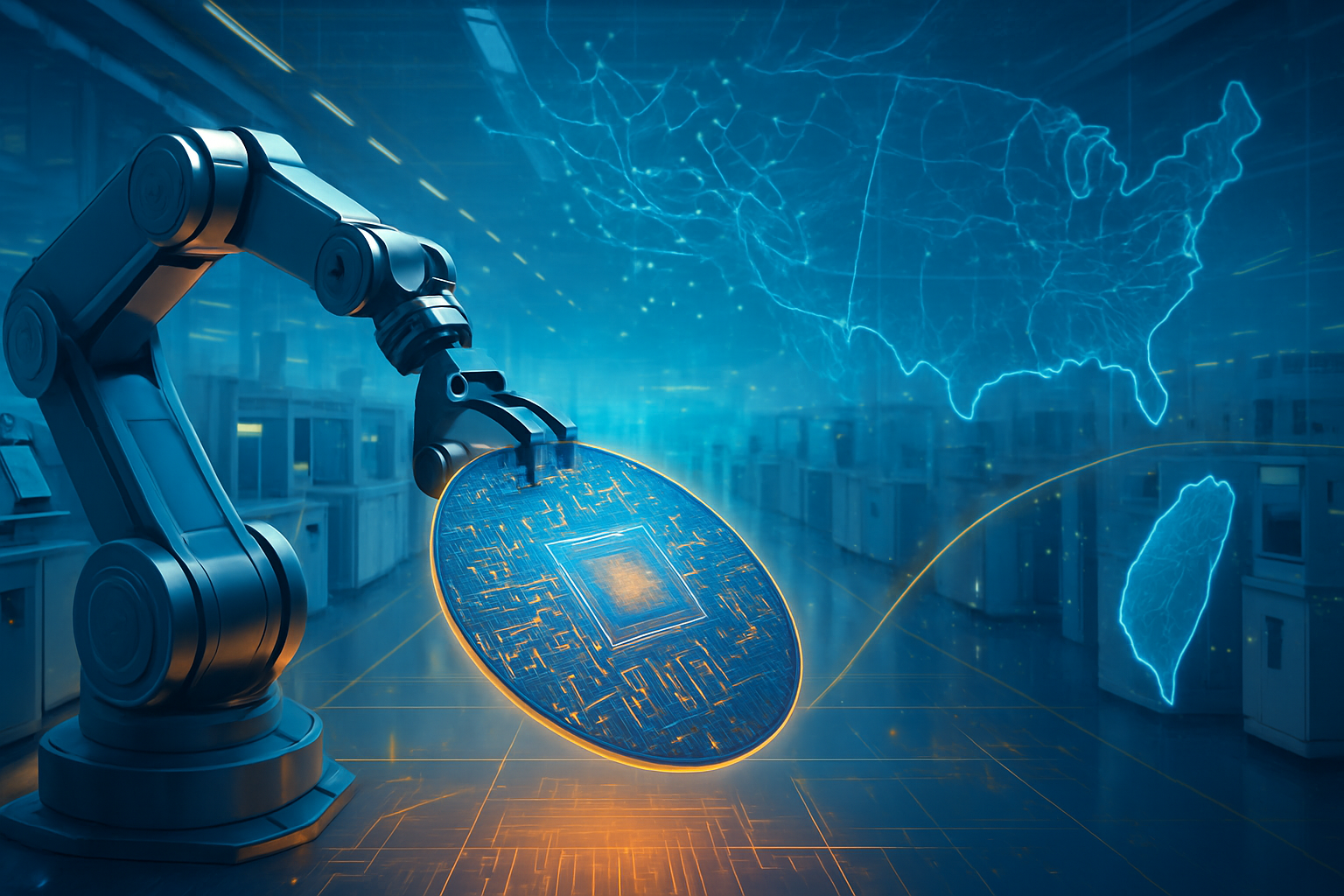
    The strategic advantage for 2026 belongs to those who have vertically integrated or secured long-term capacity agreements. Companies like Amkor Technology (NASDAQ: AMKR) have seen their stock soar as they take on "overflow" 2.5D packaging tasks that TSMC no longer has the bandwidth to handle. However, the reliance on Taiwan remains the industry's greatest vulnerability. While TSMC is expanding into Arizona and Japan, those facilities are still primarily focused on wafer fabrication; the most advanced CoWoS-L and SoIC assembly remains concentrated in Taiwan's AP6 and AP7 fabs, leaving the global AI economy tethered to the geopolitical stability of the Taiwan Strait.

    A Choke Point Within a Choke Point: The Broader AI Landscape

    The 2026 CoWoS crisis is a symptom of a broader trend: the "physicalization" of the AI boom. For years, the narrative around AI focused on software, neural network architectures, and data. Today, the limiting factor is the physical reality of atoms, heat, and microscopic wires. This packaging bottleneck has effectively created a "hard ceiling" on the growth of the global AI compute capacity. Even if the world could build a dozen more "Giga-fabs" to print silicon wafers, they would still sit idle without the specialized "pick-and-place" and bonding equipment required to finish the chips.

    This development has profound impacts on the AI landscape, particularly regarding the cost of entry. The capital expenditure required to secure a spot in the CoWoS queue is so high that it is accelerating the consolidation of AI power into the hands of a few trillion-dollar entities. This "packaging tax" is being passed down to consumers and enterprise clients, keeping the cost of training Large Language Models (LLMs) high and potentially slowing the democratization of AI. Furthermore, it has spurred a new wave of innovation in "packaging-efficient" AI, where researchers are looking for ways to achieve high performance using smaller, more easily packaged chips rather than the massive "Super-Chips" that currently dominate the market.

    Comparatively, the 2026 packaging crisis mirrors the oil shocks of the 1970s—a realization that a vital global resource is controlled by a tiny number of suppliers and subject to extreme physical constraints. This has led to a surge in government subsidies for "Backend" manufacturing, with the US CHIPS Act and similar European initiatives finally prioritizing packaging plants as much as wafer fabs. The realization has set in: a chip is not a chip until it is packaged, and without that final step, the "Silicon Intelligence" remains trapped in the wafer.

    Looking Ahead: Panel-Level Packaging and the 2027 Roadmap

    The near-term solution to the 2026 bottleneck involves the massive expansion of TSMC’s Advanced Backend Fab 7 (AP7) in Chiayi and the repurposing of former display panel plants for "AP8." However, the long-term future of the industry lies in a transition from Wafer-Level Packaging to Fan-Out Panel-Level Packaging (FOPLP). By using large rectangular panels instead of circular 300mm wafers, manufacturers can increase the number of chips processed in a single batch by up to 300%. TSMC and its partners are already conducting pilot runs for FOPLP, with expectations that it will become the high-volume standard by late 2027 or 2028.

    Another major hurdle on the horizon is the transition to "Glass Substrates." As the number of chiplets on a single package increases, the organic substrates currently in use are reaching their limits of structural integrity and electrical performance. Intel has taken an early lead in glass substrate research, which could allow for even denser interconnects and better thermal management. If successful, this could be the catalyst that allows Intel to break TSMC's packaging monopoly in the latter half of the decade. Experts predict that the winner of the "Glass Race" will likely dominate the 2028-2030 AI hardware cycle.

    Conclusion: The Final Frontier of Moore's Law

    The current state of advanced packaging represents a fundamental shift in the history of computing. As of January 2026, the industry has accepted that the future of AI does not live on a single piece of silicon, but in the sophisticated "cities" of chiplets built through CoWoS and its successors. TSMC’s ability to scale this technology has made it the most indispensable company in the world, yet the extreme concentration of this capability has created a fragile equilibrium for the global economy.

    For the coming months, the industry will be watching two key indicators: the yield rates of HBM4 integration and the speed at which TSMC can bring its AP7 Phase 2 capacity online. Any delay in these areas will have a cascading effect, delaying the release of next-generation AI models and cooling the current investment cycle. In the 2020s, we learned that data is the new oil; in 2026, we are learning that advanced packaging is the refinery. Without it, the "crude" silicon of the AI revolution remains useless.


    This content is intended for informational purposes only and represents analysis of current AI developments.

    TokenRing AI delivers enterprise-grade solutions for multi-agent AI workflow orchestration, AI-powered development tools, and seamless remote collaboration platforms.
    For more information, visit https://www.tokenring.ai/.

  • The Backside Revolution: How Intel’s PowerVia Architecture is Solving the AI ‘Power Wall’

    The Backside Revolution: How Intel’s PowerVia Architecture is Solving the AI ‘Power Wall’

    The semiconductor industry has reached a historic inflection point in January 2026, as the "Great Flip" from front-side to backside power delivery becomes the defining standard for the sub-2nm era. At the heart of this architectural shift is Intel Corporation (NASDAQ: INTC) and its proprietary PowerVia technology. By moving a chip’s power delivery network to the "backside" of the silicon wafer, Intel has effectively decoupled power and signaling—a move that industry experts describe as the most significant change to transistor architecture since the introduction of FinFET over a decade ago.

    As of early 2026, the success of the Intel 18A node has validated this risky bet. By being the first to commercialize backside power delivery (BSPD) in high-volume manufacturing, Intel has not only hit its ambitious "five nodes in four years" target but has also provided a critical lifeline for the AI industry. With high-end AI accelerators now pushing toward 1,000-watt power envelopes, traditional front-side wiring had hit a "power wall" where electrical resistance and congestion were stalling performance gains. PowerVia has shattered this wall, enabling the massive transistor densities and energy efficiencies required for the next generation of trillion-parameter large language models (LLMs).

    The Engineering Behind the 'Great Flip'

    The technical genius of PowerVia lies in how it addresses IR drop—the phenomenon where voltage decreases as it travels through a chip’s complex internal wiring. In traditional designs, both power and data signals compete for space in a "spaghetti" of metal layers stacked on top of the transistors. As transistors shrink toward 2nm and beyond, these wires become so thin and crowded that they generate excessive heat and lose significant voltage before reaching their destination. PowerVia solves this by relocating the entire power grid to the underside of the silicon wafer.

    This architecture utilizes Nano-TSVs (Through-Silicon Vias), which are roughly 500 times smaller than standard TSVs, to connect the backside power rails directly to the transistors. According to results from Intel’s Blue Sky Creek test chip, this method reduces platform voltage droop by a staggering 30% and allows for more than 90% cell utilization. By removing the bulky power wires from the front side, engineers can now use "relaxed" wiring for signals, reducing interference and allowing for a 6% boost in clock frequencies without any changes to the underlying transistor design.

    This shift represents a fundamental departure from the manufacturing processes used by Taiwan Semiconductor Manufacturing Company (NYSE: TSM) and Samsung Electronics (KRX: 005930) in their previous 3nm and early 2nm nodes. While competitors have relied on optimizing the existing front-side stack, Intel’s decision to move to the backside required mastering a complex process of wafer flipping, thinning the silicon to a few micrometers, and achieving nanometer-scale alignment for the Nano-TSVs. The successful yields reported this month on the 18A node suggest that Intel has solved the structural integrity and alignment issues that many feared would delay the technology.

    A New Competitive Paradigm for Foundries

    The commercialization of PowerVia has fundamentally altered the competitive landscape of the semiconductor market in 2026. Intel currently holds a 1.5-to-2-year "first-mover" advantage over TSMC, whose equivalent technology, the A16 Super Power Rail, is only now entering risk production. This lead has allowed Intel Foundry Services (IFS) to secure massive contracts from tech giants looking to diversify their supply chains. Microsoft Corporation (NASDAQ: MSFT) has become a flagship customer, utilizing the 18A node for its Maia 2 AI accelerator to manage the intense power requirements of its Azure AI infrastructure.

    Perhaps the most significant market shift is the strategic pivot by NVIDIA Corporation (NASDAQ: NVDA). While NVIDIA continues to rely on TSMC for its highest-end GPU production, it recently finalized a $5 billion co-development deal with Intel to leverage PowerVia and advanced Foveros packaging for next-generation server CPUs. This multi-foundry approach highlights a new reality: in 2026, manufacturing location and architectural efficiency are as important as pure transistor size. Intel’s ability to offer a "National Champion" manufacturing base on U.S. soil, combined with its lead in backside power, has made it a credible alternative to TSMC for the world's most demanding AI silicon.

    Samsung Electronics is also in the fray, attempting to leapfrog the industry by pulling forward its SF2Z node, which integrates its own version of backside power. However, as of January 2026, Intel’s high-volume manufacturing (HVM) status gives it the upper hand in "de-risking" the technology for risk-averse chip designers. Electronic Design Automation (EDA) leaders like Synopsys (NASDAQ: SNPS) and Cadence Design Systems (NASDAQ: CDNS) have already integrated PowerVia-specific tools into their suites, further cementing Intel’s architectural lead in the design ecosystem.

    Breaking the AI Thermal Ceiling

    The wider significance of PowerVia extends beyond mere manufacturing specs; it is a critical enabler for the future of AI. As AI models become more "agentic" and complex, the chips powering them have faced an escalating thermal crisis. By thinning the silicon wafer to accommodate backside power, manufacturers have inadvertently created a more efficient thermal path. The heat-generating transistors are now physically closer to the cooling solutions on the back of the chip, making advanced liquid-cooling and microfluidic integration much more effective.

    This architectural shift has also allowed for a massive increase in logic density. By "de-cluttering" the front side of the chip, manufacturers can pack more specialized Neural Processing Units (NPUs) and larger SRAM caches into the same physical footprint. For AI researchers, this translates to chips that can handle more parameters on-device, reducing the latency for real-time AI applications. The 30% area reduction offered by the 18A node means that the 2026 generation of smartphones and laptops can run sophisticated LLMs that previously required data center connectivity.

    However, the transition has not been without concerns. The extreme precision required to bond and thin wafers has led to higher initial costs, widening the "compute divide" between well-funded tech giants and smaller startups. Furthermore, the concentration of power on the backside creates intense localized "hot spots" that require a new generation of cooling technologies, such as diamond-based heat spreaders. Despite these challenges, the consensus among the AI research community is that PowerVia was the necessary price of admission for the Angstrom era of computing.

    The Road to Sub-1nm and Beyond

    Looking ahead, the success of PowerVia is just the first step in a broader roadmap toward three-dimensional vertical stacking. Intel is already sharing design kits for its 14A node, which will introduce PowerDirect—a second-generation backside technology that connects power directly to the source and drain of the transistor, further reducing resistance. Experts predict that by 2028, the industry will move toward "backside signaling," where non-critical data paths are also moved to the back, leaving the front side exclusively for high-speed logic and optical interconnects.

    The next major milestone to watch is the integration of PowerVia with High-NA EUV (Extreme Ultraviolet) lithography. This combination will allow for even finer transistor features and is expected to be the foundation for the 10A node later this decade. Challenges remain in maintaining high yields as the silicon becomes thinner and more fragile, but the industry's rapid adoption of backside-aware EDA tools suggests that the design hurdles are being cleared faster than anticipated.

    A Legacy of Innovation in the AI Era

    In summary, Intel’s PowerVia represents one of the most successful "comeback" stories in the history of silicon manufacturing. By identifying the power delivery bottleneck early and committing to a radical architectural change, Intel has reclaimed its position as a technical pioneer. The successful ramp-up of the 18A node in early 2026 marks the end of the "spaghetti" era of chip design and the beginning of a new 3D paradigm that treats both sides of the wafer as active real estate.

    For the tech industry, the implications are clear: the power wall has been breached. As we move further into 2026, the focus will shift from whether backside power works to how quickly it can be scaled across all segments of computing. Investors and analysts should keep a close eye on the performance of Intel’s "Panther Lake" and "Clearwater Forest" chips in the coming months, as these will be the ultimate barometers for PowerVia’s impact on the global AI economy.


    This content is intended for informational purposes only and represents analysis of current AI developments.

    TokenRing AI delivers enterprise-grade solutions for multi-agent AI workflow orchestration, AI-powered development tools, and seamless remote collaboration platforms.
    For more information, visit https://www.tokenring.ai/.

  • The Glass Revolution: How Intel’s High-Volume Glass Substrates Are Unlocking the Next Era of AI Scale

    The Glass Revolution: How Intel’s High-Volume Glass Substrates Are Unlocking the Next Era of AI Scale

    The semiconductor industry reached a historic milestone this month as Intel Corporation (NASDAQ: INTC) officially transitioned its glass substrate technology into high-volume manufacturing (HVM). Announced during CES 2026, the shift from traditional organic materials to glass marks the most significant change in chip packaging in over two decades. By moving beyond the physical limitations of organic resin, Intel has successfully launched the Xeon 6+ "Clearwater Forest" processor, the first commercial product to utilize a glass core, signaling a new era for massive AI systems-on-package (SoP).

    This development is not merely a material swap; it is a structural necessity for the survival of Moore’s Law in the age of generative AI. As artificial intelligence models demand increasingly larger silicon footprints and more high-bandwidth memory (HBM), the industry had hit a "warpage wall" with traditional organic substrates. Intel’s leap into glass provides the mechanical rigidity and thermal stability required to build the "reticle-busting" chips of the future, enabling interconnect densities that were previously thought to be impossible outside of a laboratory setting.

    Breaking the Warpage Wall: The Technical Leap to Glass

    For years, the industry relied on organic substrates—specifically Ajinomoto Build-up Film (ABF)—which are essentially high-tech plastics. While cost-effective, organic materials expand and contract at different rates than the silicon chips sitting on top of them, a phenomenon known as Coefficient of Thermal Expansion (CTE) mismatch. In the high-heat environment of a 1,000-watt AI accelerator, this causes the substrate to warp, cracking the microscopic solder bumps that connect the chip to the board. Glass, however, possesses a CTE that nearly matches silicon. This allows Intel to manufacture packages exceeding 100mm x 100mm without the risk of mechanical failure, providing a perfectly flat "optical" surface with less than 1 micrometer of roughness.

    The most transformative technical achievement lies in the Through Glass Vias (TGVs). Intel’s new manufacturing process at its Chandler, Arizona facility allows for a 10-fold increase in interconnect density compared to organic substrates. These ultra-fine TGVs enable pitch widths of less than 10 micrometers, allowing thousands of additional pathways for data to travel between compute chiplets and memory stacks. Furthermore, glass is an exceptional insulator, leading to a 40% reduction in signal loss and a nearly 50% improvement in power delivery efficiency. This technical trifecta—flatness, density, and efficiency—allows for the integration of up to 12 HBM4 stacks alongside multiple compute tiles, creating a singular, massive AI engine.

    Initial reactions from the AI hardware community have been overwhelmingly positive. Research analysts at the Interuniversity Microelectronics Centre (IMEC) noted that the transition to glass represents a "paradigm shift" in how we define a processor. By moving the complexity of the interconnect into the substrate itself, Intel has effectively turned the packaging into a functional part of the silicon architecture, rather than just a protective shell.

    Competitive Stakes and the Global Race for "Panel-Level" Dominance

    While Intel currently holds a clear first-mover advantage with its 2026 HVM rollout, other industry titans are racing to catch up. Taiwan Semiconductor Manufacturing Co. (NYSE: TSM) recently accelerated its own glass roadmap, unveiling the CoPoS (Chip-on-Panel-on-Substrate) platform. However, TSMC’s mass production is not expected until late 2028, as the foundry giant remains focused on maximizing its current silicon-based CoWoS (Chip-on-Wafer-on-Substrate) capacity to meet the relentless demand for NVIDIA GPUs. This window gives Intel a strategic opportunity to win back high-performance computing (HPC) clients who are outgrowing the size limits of silicon interposers.

    Samsung Electronics (KRX: 005930) has also entered the fray, announcing a "Triple Alliance" at CES 2026 that leverages its display division’s glass-handling expertise and its semiconductor division’s HBM4 production. Samsung aims to reach mass production by the end of 2026, positioning itself as a "one-stop shop" for custom AI ASICs. Meanwhile, the SK Hynix (KRX: 000660) subsidiary Absolics is finalizing its specialized facility in Georgia, USA, with plans to provide glass substrates to companies like AMD (NASDAQ: AMD) by mid-2026.

    The implications for the market are profound. Intel’s lead in glass technology could make its foundry services (IFS) significantly more attractive to AI startups and hyperscalers like Amazon (NASDAQ: AMZN) and Google (NASDAQ: GOOGL), who are designing their own custom silicon. As AI models scale toward trillions of parameters, the ability to pack more compute power into a single, thermally stable package becomes the primary competitive differentiator in the data center market.

    The Broader AI Landscape: Efficiency in the Era of Giant Models

    The shift to glass substrates is a direct response to the "energy crisis" facing the AI industry. As training clusters grow to consume hundreds of megawatts, the inefficiency of traditional packaging has become a bottleneck. By reducing signal loss and improving power delivery, glass substrates allow AI chips to perform more calculations per watt. This fits into a broader trend of "system-level" optimization, where performance gains are no longer coming from shrinking transistors alone, but from how those transistors are connected and cooled within a massive system-on-package.

    This transition also mirrors previous semiconductor milestones, such as the introduction of High-K Metal Gate or FinFET transistors. Just as those technologies allowed Moore’s Law to continue when traditional planar transistors reached their limits, glass substrates solve the "packaging limit" that threatened to stall the growth of AI hardware. However, the transition is not without concerns. The manufacturing of glass substrates requires entirely new supply chains and specialized handling equipment, as glass is more brittle than organic resin during the assembly phase. Reliability over a 10-year data center lifecycle remains a point of intense study for the industry.

    Despite these challenges, the move to glass is viewed as inevitable. The ability to create "reticle-busting" designs—chips that are larger than the standard masks used in lithography—is the only way to meet the memory bandwidth requirements of future large language models (LLMs). Without glass, the physical footprint of the next generation of AI accelerators would likely be too unstable to manufacture at scale.

    The Future of Glass: From Chiplets to Integrated Photonics

    Looking ahead, the roadmap for glass substrates extends far beyond simple structural support. By 2028, experts predict the introduction of "Panel-Level Packaging," where chips are processed on massive 600mm x 600mm glass sheets, similar to how flat-panel displays are made. This would drastically reduce the cost of advanced packaging and allow for even larger AI systems that could bridge the gap between individual chips and entire server racks.

    Perhaps the most exciting long-term development is the integration of optical interconnects. Because glass is transparent, it provides a natural medium for silicon photonics. Future iterations of Intel’s glass substrates are expected to include integrated optical wave-guides, allowing chips to communicate using light instead of electricity. This would virtually eliminate data latency and power consumption for chip-to-chip communication, paving the way for the first truly "planetary-scale" AI computers.

    While the industry must still refine the yields of these complex glass structures, the momentum is irreversible. Engineers are already working on the next generation of 14A process nodes that will rely exclusively on glass-based architectures to handle the massive power densities of the late 2020s.

    A New Foundation for Artificial Intelligence

    The launch of Intel’s high-volume glass substrate manufacturing marks a definitive turning point in computing history. It represents the moment the industry moved beyond the "plastic" era of the 20th century into a "glass" era designed specifically for the demands of artificial intelligence. By solving the critical issues of thermal expansion and interconnect density, Intel has provided the physical foundation upon which the next decade of AI breakthroughs will be built.

    As we move through 2026, the industry will be watching the yields and field performance of the Xeon 6+ "Clearwater Forest" chips closely. If the performance and reliability gains hold, expect a rapid migration as NVIDIA, AMD, and the hyperscalers scramble to adopt glass for their own flagship products. The "Glass Age" of semiconductors has officially begun, and it is clear that the future of AI will be transparent, flat, and more powerful than ever before.


    This content is intended for informational purposes only and represents analysis of current AI developments.

    TokenRing AI delivers enterprise-grade solutions for multi-agent AI workflow orchestration, AI-powered development tools, and seamless remote collaboration platforms.
    For more information, visit https://www.tokenring.ai/.

  • Hell Freezes Over: Intel and AMD Unite to Save the x86 Empire from ARM’s Rising Tide

    Hell Freezes Over: Intel and AMD Unite to Save the x86 Empire from ARM’s Rising Tide

    In a move once considered unthinkable in the cutthroat world of semiconductor manufacturing, lifelong rivals Intel Corporation (NASDAQ: INTC) and Advanced Micro Devices, Inc. (NASDAQ: AMD) have solidified their "hell freezes over" alliance through the x86 Ecosystem Advisory Group (EAG). Formed in late 2024 and reaching a critical technical maturity in early 2026, this partnership marks a strategic pivot from decades of bitter competition to a unified front. The objective is clear: defend the aging but dominant x86 architecture against the relentless encroachment of ARM-based silicon, which has rapidly seized territory in both the high-end consumer laptop and hyper-scale data center markets.

    The significance of this development cannot be overstated. For forty years, Intel and AMD defined their success by their differences, often introducing incompatible instruction set extensions that forced software developers to choose sides or write complex, redundant code. Today, the x86 EAG—which includes a "founding board" of industry titans such as Microsoft Corporation (NASDAQ: MSFT), Alphabet Inc. (NASDAQ: GOOGL), Meta Platforms, Inc. (NASDAQ: META), and Broadcom Inc. (NASDAQ: AVGO)—represents a collective realization that the greatest threat to their future is no longer each other, but the energy-efficient, highly customizable architecture of the ARM ecosystem.

    Standardizing the Instruction Set: A Technical Renaissance

    The technical cornerstone of this alliance is a commitment to "consistent innovation," which aims to eliminate the fragmentation that has plagued the x86 instruction set architecture (ISA) for years. Leading into 2026, the group has finalized the specifications for AVX10, a unified vector instruction set that solves the long-standing "performance vs. efficiency" core dilemma. Unlike previous versions of AVX-512, which were often disabled on hybrid chips to maintain consistency across cores, AVX10 allows high-performance AI and scientific workloads to run seamlessly across all processor types, ensuring developers no longer have to navigate the "ISA tax" of targeting different hardware features within the same ecosystem.

    Beyond vector processing, the advisory group has introduced critical security and system modernizations. A standout feature is ChkTag (x86 Memory Tagging), a hardware-level security layer designed to combat buffer overflows and memory-corruption vulnerabilities. This is a direct response to ARM's Memory Tagging Extension (MTE), which has become a selling point for security-conscious enterprise clients. Additionally, the alliance has pushed forward the Flexible Return and Event Delivery (FRED) framework, which overhauls how CPUs handle interrupts—a legacy system that had not seen a major update since the 1980s. By streamlining these low-level operations, Intel and AMD are significantly reducing system latency and improving reliability in virtualized cloud environments.

    This unified approach differs fundamentally from the proprietary roadmaps of the past. Historically, Intel might introduce a feature like Intel AMX, only for it to remain unavailable on AMD hardware for years, leaving developers hesitant to adopt it. By folding initiatives like the "x86-S" simplified architecture into the EAG, the two giants are ensuring that major changes—such as the eventual removal of 16-bit and 32-bit legacy support—happen in lockstep. This coordinated evolution provides software vendors like Adobe or Epic Games with a stable, predictable target for the next decade of computing.

    Initial reactions from the technical community have been cautiously optimistic. Linus Torvalds, the creator of Linux and a technical advisor to the group, has noted that a more predictable x86 architecture simplifies kernel development immensely. However, industry experts point out that while standardizing the ISA is a massive step forward, the success of the EAG will ultimately depend on whether Intel and AMD can match the "performance-per-watt" benchmarks set by modern ARM designs. The era of brute-force clock speeds is over; the alliance must now prove that x86 can be as lean as it is powerful.

    The Competitive Battlefield: AI PCs and Cloud Sovereignty

    The competitive implications of this alliance ripple across the entire tech sector, particularly benefiting the "founding board" members who oversee the world’s largest software ecosystems. For Microsoft, a unified x86 roadmap ensures that Windows 11 and its successors can implement deep system-level optimizations that work across the vast majority of the PC market. Similarly, server-side giants like Dell Technologies Inc. (NYSE: DELL), HP Inc. (NYSE: HPQ), and Hewlett Packard Enterprise (NYSE: HPE) gain a more stable platform to market to enterprise clients who are increasingly tempted by the custom ARM chips of cloud providers.

    On the other side of the fence, the alliance is a direct challenge to the momentum of Apple Inc. (NASDAQ: AAPL) and Qualcomm Incorporated (NASDAQ: QCOM). Apple’s transition to its M-series silicon demonstrated that a tightly integrated, ARM-based stack could deliver industry-leading efficiency, while Qualcomm’s Snapdragon X series has brought competitive battery life to the Windows ecosystem. By modernizing x86, Intel and AMD are attempting to neutralize the "legacy bloat" argument that ARM proponents have used to win over OEMs. If the EAG succeeds in making x86 chips significantly more efficient, the strategic advantage currently held by ARM in the "always-connected" laptop space could evaporate.

    Hyperscalers like Amazon.com, Inc. (NASDAQ: AMZN) and Google stand in a complex position. While they sit on the EAG board, they also develop their own ARM-based processors like Graviton and Axion to reduce their reliance on third-party silicon. However, the x86 alliance provides these companies with a powerful hedge. By ensuring that x86 remains a viable, high-performance option for their data centers, they maintain leverage in price negotiations and ensure that the massive library of legacy enterprise software—which remains predominantly x86-based—continues to run optimally on their infrastructure.

    For the broader AI landscape, the alliance's focus on Advanced Matrix Extensions (ACE) provides a strategic advantage for on-device AI. As AI PCs become the standard in 2026, having a standardized instruction set for matrix multiplication ensures that AI software developers don't have to optimize their models separately for Intel Core Ultra and AMD Ryzen processors. This standardization could potentially disrupt the specialized NPU (Neural Processing Unit) market, as more AI tasks are efficiently offloaded to the standardized, high-performance CPU cores.

    A Strategic Pivot in Computing History

    The x86 Ecosystem Advisory Group arrives at a pivotal moment in the broader history of computing, echoing the seismic shifts seen during the transition from 32-bit to 64-bit architecture. For decades, the tech industry operated under the assumption that x86 was the permanent king of the desktop and server, while ARM was relegated to mobile devices. That boundary has been permanently shattered. The Intel-AMD alliance is a formal acknowledgment that the "Wintel" era of unchallenged dominance has ended, replaced by an era where architecture must justify its existence through efficiency and developer experience rather than just market inertia.

    This development is particularly significant in the context of the current AI revolution. The demand for massive compute power has traditionally favored x86’s raw performance, but the high energy costs of AI data centers have made ARM’s efficiency increasingly attractive. By collaborating to strip away legacy baggage and standardize AI-centric instructions, Intel and AMD are attempting to bridge the gap between "big iron" performance and modern efficiency requirements. It is a defensive maneuver, but one that is being executed with an aggressive focus on the future of the AI-native cloud.

    There are, however, potential concerns regarding the "duopoly" nature of this alliance. While the involvement of companies like Google and Meta is intended to provide a check on Intel and AMD’s power, some critics worry that a unified x86 standard could stifle niche architectural innovations. Comparisons are being drawn to the early days of the USB or PCIe standards—while they brought order to chaos, they also shifted the focus from radical breakthroughs to incremental, consensus-based updates.

    Ultimately, the EAG represents a shift from "competition through proprietary lock-in" to "competition through execution." By commoditizing the instruction set, Intel and AMD are betting that they can win based on who builds the best transistors, the most efficient power delivery systems, and the most advanced packaging, rather than who has the most unique (and frustrating) software extensions. It is a gamble that the x86 ecosystem is stronger than the sum of its rivals.

    Future Roadmaps: Scaling the AI Wall

    Looking ahead to the remainder of 2026 and into 2027, the first "EAG-compliant" silicon is expected to hit the market. These processors will be the true test of the alliance, featuring the finalized AVX10 and FRED standards out of the box. Near-term developments will likely focus on the "64-bit only" transition, with the group expected to release a formal timeline for the phasing out of native 16-bit and 32-bit hardware support. This will allow for even leaner chip designs, as silicon real estate currently dedicated to legacy compatibility is reclaimed for more cache or additional AI accelerators.

    In the long term, we can expect the x86 EAG to explore deeper integration with the software stack. There is significant speculation that the group is working on a "Universal Binary" format for Windows and Linux that would allow a single compiled file to run with maximum efficiency on any x86 chip from any vendor, effectively matching the seamless experience of the ARM-based macOS ecosystem. Challenges remain, particularly in ensuring that the many disparate members of the advisory group remain aligned as their individual business interests inevitably clash.

    Experts predict that the success of this alliance will dictate whether x86 remains the backbone of the enterprise world for the next thirty years or if it eventually becomes a legacy niche. If the EAG can successfully deliver on its promise of a modernized, unified, and efficient architecture, it will likely slow the migration to ARM significantly. However, if the group becomes bogged down in committee-level bureaucracy, the agility of the ARM ecosystem—and the rising challenge of the open-source RISC-V architecture—may find an even larger opening to exploit.

    Conclusion: The New Era of Unified Silicon

    The formation and technical progress of the x86 Ecosystem Advisory Group represent a watershed moment in the semiconductor industry. By uniting against a common threat, Intel and AMD have effectively ended a forty-year civil war to preserve the legacy and future of the architecture that powered the digital age. The key takeaways from this alliance are the standardization of AI and security instructions, the coordinated removal of legacy bloat, and the unprecedented collaboration between silicon designers and software giants to create a unified developer experience.

    As we look at the history of AI and computing, this alliance will likely be remembered as the moment when the "old guard" finally adapted to the realities of a post-mobile, AI-first world. The significance lies not just in the technical specifications, but in the cultural shift: the realization that in a world of custom silicon and specialized accelerators, the ecosystem is the ultimate product.

    In the coming weeks and months, industry watchers should look for the first third-party benchmarks of AVX10-enabled software and any announcements regarding the next wave of members joining the advisory group. As the first EAG-optimized servers begin to roll out to data centers in mid-2026, we will see the first real-world evidence of whether this "hell freezes over" pact is enough to keep the x86 crown from slipping.


    This content is intended for informational purposes only and represents analysis of current AI developments.

    TokenRing AI delivers enterprise-grade solutions for multi-agent AI workflow orchestration, AI-powered development tools, and seamless remote collaboration platforms.
    For more information, visit https://www.tokenring.ai/.

  • The Silicon Glue: 2026 HBM4 Sampling and the Global Alliance Ending the AI Memory Bottleneck

    The Silicon Glue: 2026 HBM4 Sampling and the Global Alliance Ending the AI Memory Bottleneck

    As of January 19, 2026, the artificial intelligence industry is witnessing an unprecedented capital expenditure surge centered on a single, critical component: High-Bandwidth Memory (HBM). With the transition from HBM3e to the revolutionary HBM4 standard reaching a fever pitch, the "memory wall"—the performance gap between ultra-fast logic processors and slower data storage—is finally being dismantled. This shift is not merely an incremental upgrade but a structural realignment of the semiconductor supply chain, led by a powerhouse alliance between SK Hynix (KRX: 000660), TSMC (NYSE: TSM), and NVIDIA (NASDAQ: NVDA).

    The immediate significance of this development cannot be overstated. As large-scale AI models move toward the 100-trillion parameter threshold, the ability to feed data to GPUs has become the primary constraint on performance. The massive investments announced this month by the world’s leading memory makers indicate that the industry has entered a "supercycle" phase, where HBM is no longer treated as a commodity but as a customized, high-value logic component essential for the survival of the AI era.

    The HBM4 Revolution: 2048-bit Interfaces and Active Memory

    The HBM4 transition, currently entering its critical sampling phase in early 2026, represents the most significant architectural change in memory technology in over a decade. Unlike HBM3e, which utilized a 1024-bit interface, HBM4 doubles the bus width to a staggering 2048-bit interface. This "wider pipe" allows for massive data throughput—targeted at up to 3.25 TB/s per stack—without requiring the extreme clock speeds that have plagued previous generations with thermal and power efficiency issues. By doubling the interface width, manufacturers can achieve higher performance at lower power consumption, a critical factor for the massive AI "factories" being built by hyperscalers.

    Furthermore, the introduction of "active" memory marks a radical departure from traditional DRAM manufacturing. For the first time, the base die (or logic die) at the bottom of the HBM stack is being manufactured using advanced logic nodes rather than standard memory processes. SK Hynix has formally partnered with TSMC to produce these base dies on 5nm and 12nm processes. This allows the memory stack to gain "active" processing capabilities, effectively embedding basic logic functions directly into the memory. This "processing-near-memory" approach enables the HBM stack to handle data manipulation and sorting before it even reaches the GPU, significantly reducing latency.

    Initial reactions from the AI research community have been overwhelmingly positive. Experts suggest that the move to a 2048-bit interface and TSMC-manufactured logic dies will provide the 3x to 5x performance leap required for the next generation of multimodal AI agents. By integrating the memory and logic more closely through hybrid bonding techniques, the industry is effectively moving toward "3D Integrated Circuits," where the distinction between where data is stored and where it is processed begins to blur.

    A Three-Way Race: Market Share and Strategic Alliances

    The strategic landscape of 2026 is defined by a fierce three-way race for HBM dominance among SK Hynix, Samsung (KRX: 005930), and Micron (NASDAQ: MU). SK Hynix currently leads the market with a dominant share estimated between 53% and 62%. The company recently announced that its entire 2026 HBM capacity is already fully booked, primarily by NVIDIA for its upcoming Rubin architecture and Blackwell Ultra series. SK Hynix’s "One Team" alliance with TSMC has given it a first-mover advantage in the HBM4 generation, allowing it to provide a highly optimized "active" memory solution that competitors are now scrambling to match.

    However, Samsung is mounting a massive recovery effort. After a delayed start in the HBM3e cycle, Samsung successfully qualified its 12-layer HBM3e for NVIDIA in late 2025 and is now targeting a February 2026 mass production start for its own HBM4 stacks. Samsung’s primary strategic advantage is its "turnkey" capability; as the only company that owns both world-class DRAM production and an advanced semiconductor foundry, Samsung can produce the HBM stacks and the logic dies entirely in-house. This vertical integration could theoretically offer lower costs and tighter design cycles once their 4nm logic die yields stabilize.

    Meanwhile, Micron has solidified its position as a critical third pillar in the supply chain, controlling approximately 15% to 21% of the market. Micron’s aggressive move to establish a "Megafab" in New York and its early qualification of 12-layer HBM3e have made it a preferred partner for companies seeking to diversify their supply away from the SK Hynix/TSMC duopoly. For NVIDIA and AMD (NASDAQ: AMD), this fierce competition is a massive benefit, ensuring a steady supply of high-performance silicon even as demand continues to outstrip supply. However, smaller AI startups may face a "memory drought," as the "Big Three" have largely prioritized long-term contracts with trillion-dollar tech giants.

    Beyond the Memory Wall: Economic and Geopolitical Shifts

    The massive investment in HBM fits into a broader trend of "hardware-software co-design" that is reshaping the global tech landscape. As AI models transition from static LLMs into proactive agents capable of real-world reasoning, the "Memory Wall" has replaced raw compute power as the most significant hurdle for AI scaling. The 2026 HBM surge reflects a realization across the industry that the bottleneck for artificial intelligence is no longer just FLOPS (floating-point operations per second), but the "communication cost" of moving data between memory and logic.

    The economic implications are profound, with the total HBM market revenue projected to reach nearly $60 billion in 2026. This is driving a significant relocation of the semiconductor supply chain. SK Hynix’s $4 billion investment in an advanced packaging plant in Indiana, USA, and Micron’s domestic expansion represent a strategic shift toward "onshoring" critical AI components. This move is partly driven by the need to be closer to US-based design houses like NVIDIA and partly by geopolitical pressures to secure the AI supply chain against regional instabilities.

    However, the concentration of this technology in the hands of just three memory makers and one leading foundry (TSMC) raises concerns about market fragility. The high cost of entry—requiring billions in specialized "Advanced Packaging" equipment and cleanrooms—means that the barrier to entry for new competitors is nearly insurmountable. This reinforces a global "AI arms race" where nations and companies without direct access to the HBM4 supply chain may find themselves technologically sidelined as the gap between state-of-the-art AI and "commodity" AI continues to widen.

    The Road to Half-Terabyte GPUs and HBM5

    Looking ahead through the remainder of 2026 and into 2027, the industry expects the first volume shipments of 16-layer (16-Hi) HBM4 stacks. These stacks are expected to provide up to 64GB of memory per "cube." In an 8-stack configuration—which is rumored for NVIDIA’s upcoming Rubin platform—a single GPU could house a staggering 512GB of high-speed memory. This would allow researchers to train and run massive models on significantly smaller hardware footprints, potentially enabling "Sovereign AI" clusters that occupy a fraction of the space of today's data centers.

    The primary technical challenge remaining is heat dissipation. As memory stacks grow taller and logic dies become more powerful, managing the thermal profile of a 16-layer stack will require breakthroughs in liquid-to-chip cooling and hybrid bonding techniques that eliminate the need for traditional "bumps" between layers. Experts predict that if these thermal hurdles are cleared, the industry will begin looking toward HBM4E (Extended) by late 2027, which will likely integrate even more complex AI accelerators directly into the memory base.

    Beyond 2027, the roadmap for HBM5 is already being discussed in research circles. Early predictions suggest HBM5 may transition from electrical interconnects to optical interconnects, using light to move data between the memory and the processor. This would essentially eliminate the bandwidth bottleneck forever, but it requires a fundamental rethink of how silicon chips are designed and manufactured.

    A Landmark Shift in Semiconductor History

    The HBM explosion of 2026 is a watershed moment for the semiconductor industry. By breaking the memory wall, the triad of SK Hynix, TSMC, and NVIDIA has paved the way for a new era of AI capability. The transition to HBM4 marks the point where memory stopped being a passive storage bin and became an active participant in computation. The shift from commodity DRAM to customized, logic-integrated HBM is the most significant change in memory architecture since the invention of the integrated circuit.

    In the coming weeks and months, the industry will be watching Samsung’s production yields at its Pyeongtaek campus and the initial performance benchmarks of the first HBM4 engineering samples. As 2026 progresses, the success of these HBM4 rollouts will determine which tech giants lead the next decade of AI innovation. The memory bottleneck is finally yielding, and with it, the limits of what artificial intelligence can achieve are being redefined.


    This content is intended for informational purposes only and represents analysis of current AI developments.

    TokenRing AI delivers enterprise-grade solutions for multi-agent AI workflow orchestration, AI-powered development tools, and seamless remote collaboration platforms.
    For more information, visit https://www.tokenring.ai/.

  • Silicon Bridge: The Landmark US-Taiwan Accord That Redefines Global AI Power

    Silicon Bridge: The Landmark US-Taiwan Accord That Redefines Global AI Power

    The global semiconductor landscape underwent a seismic shift last week with the official announcement of the U.S.-Taiwan Semiconductor Trade and Investment Agreement on January 15, 2026. Signed by the American Institute in Taiwan (AIT) and the Taipei Economic and Cultural Representative Office (TECRO), the deal—informally dubbed the "Silicon Pact"—represents the most significant intervention in tech trade policy since the original CHIPS Act. At its core, the agreement formalizes a "tariff-for-investment" swap: the United States will lower existing trade barriers for Taiwanese tech in exchange for a staggering $250 billion to $465 billion in long-term manufacturing investments, primarily centered in the burgeoning Arizona "megafab" cluster.

    The deal’s immediate significance lies in its attempt to solve two problems at once: the vulnerability of the global AI supply chain and the growing trade tensions surrounding high-performance computing. By establishing a framework that incentivizes domestic production through massive tariff offsets, the U.S. is effectively attempting to pull the center of gravity for the world's most advanced chips across the Pacific. For Taiwan, the pact provides a necessary economic lifeline and a deepened strategic bond with Washington, even as it navigates the complex "Silicon Shield" dilemma that has defined its national security for decades.

    The "Silicon Pact" Mechanics: High-Stakes Trade Policy

    The technical backbone of this agreement is the revolutionary Tariff Offset Program (TOP), a mechanism designed to bypass the 25% global semiconductor tariff imposed under Section 232 on January 14, 2026. This 25% ad valorem tariff specifically targets high-end GPUs and AI accelerators, such as the NVIDIA (NASDAQ: NVDA) H200 and AMD (NASDAQ: AMD) MI325X, which are essential for training large-scale AI models. Under the new pact, Taiwanese firms building U.S. capacity receive unprecedented duty-free quotas. During the construction of a new fab, these companies can import up to 2.5 times their planned U.S. production capacity duty-free. Once a facility reaches operational status, they can continue importing 1.5 times their domestic output without paying the Section 232 duties.

    This shift represents a departure from traditional "blanket" tariffs toward a more surgical, incentive-based industrial strategy. While the U.S. share of global wafer production had dropped below 10% in late 2024, this deal aims to raise that share to 20% by 2030. For Taiwan Semiconductor Manufacturing Company (NYSE: TSM), the deal facilitates an expansion from six previously planned fabs in Arizona to a total of 11, including two dedicated advanced packaging plants. This is crucial because, until now, high-performance chips like the NVIDIA Blackwell series were fabricated in Taiwan and often shipped back to Asia for final assembly, leaving the supply chain vulnerable.

    The initial reaction from the AI research community has been cautiously optimistic. Dr. Elena Vance of the AI Policy Institute noted that while the deal may stabilize the prices of "sovereign AI" infrastructure, the administrative burden of managing these complex tariff quotas could create new bottlenecks. Industry experts have praised the move for providing a 10-year roadmap for 2nm and 1.4nm (A16) node production on U.S. soil, which was previously considered a pipe dream by many skeptics of the original 2022 CHIPS Act.

    Winners, Losers, and the Battle for Arizona

    The implications for major tech players are profound and varied. NVIDIA (NASDAQ: NVDA) stands as a primary beneficiary, with CEO Jensen Huang praising the move as a catalyst for the "AI industrial revolution." By utilizing the TOP, NVIDIA can maintain its margins on its highest-end chips while moving its supply chain into the "safe harbor" of the Phoenix-area data centers. Similarly, Apple (NASDAQ: AAPL) is expected to be the first to utilize the Arizona-made 2nm chips for its 2027 and 2028 device lineups, successfully leveraging its massive scale to secure early capacity in the new facilities.

    However, the pact creates a more complex competitive landscape for Intel (NASDAQ: INTC). While Intel benefits from the broader pro-onshoring sentiment, it now faces a direct, localized threat from TSMC’s massive expansion. Analysts at Bernstein have noted that Intel's foundry business must now compete with TSMC on its home turf, not just on technology but also on yield and pricing. Intel CEO Lip-Bu Tan has responded by accelerating the development of the Intel 18A and 14A nodes, emphasizing that "domestic competition" will only sharpen American engineering.

    The deal also shifts the strategic position of AMD (NASDAQ: AMD), which has reportedly already begun shifting its logistics toward domestic data center tenants like Riot Platforms (NASDAQ: RIOT) in Texas to bypass potential tariff escalations. For startups in the AI space, the long-term benefit may be more predictable pricing for cloud compute, provided the major providers—Microsoft (NASDAQ: MSFT) and Google (NASDAQ: GOOGL)—can successfully pass through the savings from these tariff exemptions to their customers.

    De-risking and the "Silicon Shield" Tension

    Beyond the corporate balance sheets, the US-Taiwan deal fits into a broader global trend of "technological balkanization." The imposition of the 25% tariff on non-aligned supply chains is a clear signal that the U.S. is prioritizing national security over the efficiency of the globalized "just-in-time" model. This is a "declaration of economic independence," as described by U.S. officials, aimed at eliminating dependence on East Asian manufacturing hubs that are increasingly vulnerable to geopolitical friction.

    However, concerns remain regarding the "Packaging Gap." Experts from Arete Research have pointed out that while wafer fabrication is moving to Arizona, the specialized knowledge for advanced packaging—specifically TSMC's CoWoS (Chip on Wafer on Substrate) technology—remains concentrated in Taiwan. Without a full "end-to-end" ecosystem in the U.S., the supply chain remains a "Silicon Bridge" rather than a self-contained island. If wafers still have to be shipped back to Asia for final packaging, the geopolitical de-risking remains incomplete.

    Furthermore, there is a palpable sense of irony in Taipei. For decades, Taiwan’s dominant position in the chip world—its "Silicon Shield"—has been its ultimate insurance policy. If the U.S. achieves 20% of the world’s most advanced logic production, some fear that Washington’s incentive to defend the island could diminish. This tension was likely a key driver behind the Taiwanese government's demand for $250 billion in credit guarantees as part of the deal, ensuring that the move to the U.S. is as much about mutual survival as it is about business.

    The Road to 1.4nm: What’s Next for Arizona?

    Looking ahead, the next 24 to 36 months will be critical for the execution of this deal. The first Arizona fab is already in volume production using the N4 process, but the true test will be the structural completion of the second and third fabs, which are targeted for N3 and N2 nodes by late 2027. We can expect to see a surge in specialized labor recruitment, as the 11-fab plan will require an estimated 30,000 highly skilled engineers and technicians—a workforce that the U.S. currently lacks.

    Potential applications on the horizon include the first generation of "fully domestic" AI supercomputers, which will be exempt from the 25% tariff and could serve as the foundation for the next wave of military and scientific breakthroughs. We are also likely to see a flurry of announcements from chemical and material suppliers like ASML (NASDAQ: ASML) and Applied Materials (NASDAQ: AMAT), as they build out their own service hubs in the Phoenix and Austin regions to support the new capacity.

    The challenges, however, are not just technical. Addressing the high cost of construction and energy in the U.S. will be paramount. If the "per-wafer" cost of an Arizona-made 2nm chip remains significantly higher than its Taiwanese counterpart, the U.S. government may be forced to extend these "temporary" tariffs and offsets indefinitely, creating a permanent, bifurcated market for semiconductors.

    A New Era for the Digital Age

    The January 2026 US-Taiwan semiconductor deal marks a turning point in AI history. It is the moment where the "invisible hand" of the market was replaced by the "visible hand" of industrial policy. By trading market access for physical infrastructure, the U.S. and Taiwan have fundamentally altered the path of the digital age, prioritizing resilience and national security over the cost-savings of the past three decades.

    The key takeaways from this landmark agreement are clear: the U.S. is committed to becoming a global center for advanced logic manufacturing, Taiwan remains an indispensable partner but one whose role is evolving, and the AI industry is now officially a matter of statecraft. In the coming months, the industry will be watching for the first "TOP-certified" imports and the progress of the Arizona groundbreaking ceremonies. While the "Silicon Bridge" is now under construction, its durability will depend on whether the U.S. can truly foster the deep, complex ecosystem required to sustain the world’s most advanced technology on its own soil.


    This content is intended for informational purposes only and represents analysis of current AI developments.

    TokenRing AI delivers enterprise-grade solutions for multi-agent AI workflow orchestration, AI-powered development tools, and seamless remote collaboration platforms.
    For more information, visit https://www.tokenring.ai/.