Rome, Italy – November 7, 2025 – In a landmark address delivered today at the Builders AI Forum 2025 in Rome, Pope Leo XIV issued a resounding call to Catholic technologists and venture capitalists worldwide: leverage the transformative power of artificial intelligence (AI) to advance the Church's mission of evangelization and foster the integral development of every human being. This unprecedented directive marks a pivotal moment in the intersection of faith and technology, signaling a proactive embrace of AI's potential within the spiritual realm.
The Pope's message, read by Jesuit Father David Nazar, underscored that AI, as a product of human ingenuity, can be a profound expression of humanity's participation in divine creation when guided by ethical principles. He challenged innovators to imbue AI systems with values of justice, solidarity, and respect for life, advocating for the creation of tools that can enhance Catholic education, deliver compassionate healthcare solutions, and communicate the Christian narrative with both truth and beauty. This call moves beyond mere ethical considerations of AI, directly positioning the technology as a vital instrument for spiritual outreach in an increasingly digital world.
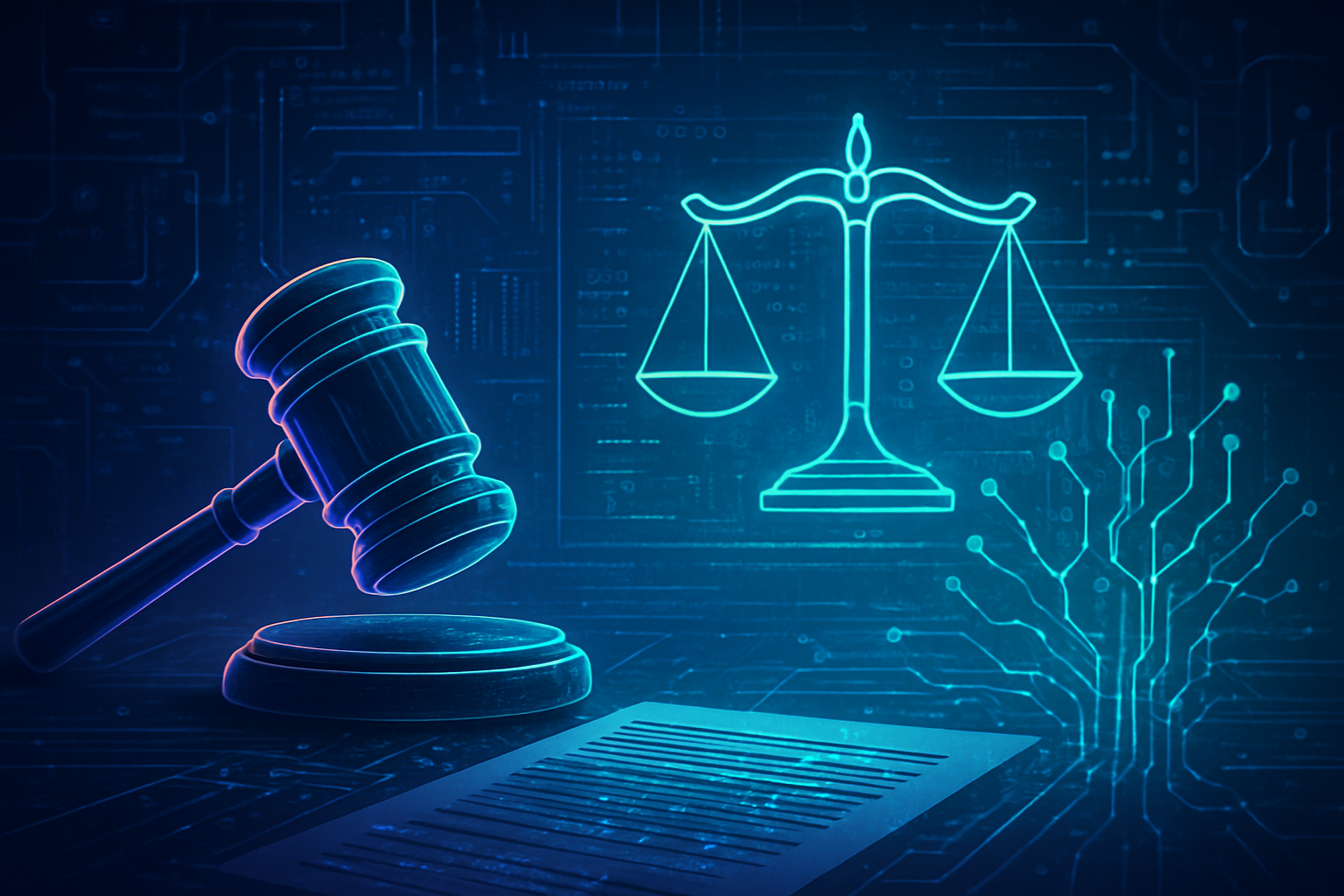
The Algorithmic Apostles: Charting AI's Evangelistic Frontiers
Pope Leo XIV's directive, articulated at the two-day Builders AI Forum 2025 at the Pontifical Gregorian University, is not a call for a single AI product but rather a foundational philosophy for integrating advanced technology into the Church's missionary efforts. The forum, drawing approximately 200 participants from software engineering, venture capital, Catholic media, and Vatican communications, explored concrete applications for "Building and Scaling Catholic AI" for evangelization. While specific technical specifications for "Catholic AI" are still nascent, the vision encompasses AI-powered platforms for personalized catechesis, intelligent translation services for scriptural texts, virtual reality experiences depicting biblical narratives, and AI assistants capable of answering theological questions in multiple languages.
This approach represents a significant departure from previous, more cautious engagements with technology by religious institutions. Historically, the Church has often reacted to technological advancements, adapting them after their widespread adoption. Pope Leo XIV's call, however, is proactive, urging the development of AI specifically designed and imbued with Catholic values from its inception. Unlike general-purpose AI, which may be repurposed for religious content, the Pope envisions systems where ethical and theological principles are "encoded into the very logic" of their design. Initial reactions from the AI research community are mixed, with some expressing enthusiasm for the ethical challenges and opportunities presented by faith-driven AI development, while others voice concerns about potential misuse or the inherent complexities of programming spiritual concepts. Experts from companies like (MSFT) Microsoft and (PLTR) Palantir Technologies, present at the forum, acknowledged the technical feasibility while recognizing the unique ethical and theological frameworks required.
The technical capabilities envisioned include natural language processing (NLP) for generating and localizing religious content, machine learning for personalizing spiritual guidance based on user interaction, and computer vision for analyzing religious art or architecture. The emphasis is on creating AI that not only disseminates information but also fosters genuine spiritual engagement, respecting the nuanced and deeply personal nature of faith. This differs from existing technologies primarily in its explicit, intentional embedding of theological and ethical discernment at every stage of AI development, rather than treating faith-based applications as mere content layers on agnostic platforms.
A New Market Frontier: AI Companies Eyeing the Sacred
Pope Leo XIV's bold vision could unlock a significant, largely untapped market for AI companies, tech giants, and startups. Companies specializing in ethical AI development, content localization, personalized learning platforms, and virtual/augmented reality stand to benefit immensely. For instance, firms like (GOOGL) Google's AI division, (MSFT) Microsoft, and (AMZN) Amazon Web Services (AWS), with their robust cloud infrastructure and AI services, could become crucial partners in providing the foundational technologies for "Catholic AI." Startups focused on niche ethical AI applications or faith-based digital tools could find unprecedented opportunities for funding and growth within this newly articulated market.
The competitive landscape for major AI labs could see a new dimension, where adherence to ethical guidelines and demonstrated commitment to human dignity, as articulated by the Vatican, become key differentiators. Companies that can effectively integrate these values into their AI development pipelines might gain a strategic advantage in securing partnerships with religious organizations globally. This development could disrupt existing product roadmaps by creating demand for specialized AI modules that prioritize moral discernment, theological accuracy, and culturally sensitive content delivery. Firms that historically focused solely on commercial applications may now explore dedicated teams or divisions for faith-based AI, positioning themselves as leaders in a new frontier of "AI for good" with a specific spiritual mandate.
Market positioning will likely shift for companies capable of demonstrating not just technological prowess but also a deep understanding and respect for religious and ethical frameworks. This could lead to new alliances between tech companies and theological institutions, fostering a collaborative environment aimed at developing AI that serves spiritual and humanitarian ends. The involvement of venture capital partners at the Builders AI Forum 2025, including representatives from (GS) Goldman Sachs, signals a growing financial interest in this emerging sector, potentially channeling significant investment into startups and initiatives aligned with the Pope's vision.
Ethical AI's Holy Grail: Navigating Faith in the Algorithmic Age
Pope Leo XIV's call fits squarely into the broader AI landscape's growing emphasis on ethical AI, AI for social good, and value-aligned technology. It elevates the discussion from general ethical principles to a specific theological framework, challenging the industry to consider how AI can serve not just human flourishing in a secular sense, but also spiritual growth and evangelization. The impacts could be profound, potentially leading to the development of AI systems that are inherently more robust against biases, designed with explicit moral guardrails, and focused on fostering community and understanding rather than mere consumption or efficiency.
However, this ambitious undertaking is not without its potential concerns. Questions immediately arise regarding the authenticity of AI-generated spiritual content, the risk of algorithmic bias in theological interpretation, data privacy for users engaging with faith-based AI, and the fundamental challenge of replicating genuine human compassion and spiritual discernment in machines. There are also theological implications to consider: can AI truly evangelize, or can it only facilitate human evangelization? The potential for AI to be misused to spread misinformation or manipulate beliefs, even with good intentions, remains a significant hurdle.
Compared to previous AI milestones, such as the development of large language models or advanced robotics, Pope Leo XIV's directive marks a unique intersection of spiritual authority and technological ambition. It's less about a technical breakthrough and more about a societal and ethical redirection of existing and future AI capabilities. It challenges the tech world to move beyond purely utilitarian applications and consider AI's role in addressing humanity's deepest questions and spiritual needs. This initiative could set a precedent for other religious traditions to explore similar applications, potentially fostering a global movement for faith-aligned AI development.
The Future of Faith: AI as a Spiritual Co-Pilot
In the near term, we can expect a surge in research and development initiatives focused on proof-of-concept AI tools for evangelization. This will likely include pilot programs for AI-powered catechetical apps, multilingual digital missionaries, and virtual pilgrimage experiences. Long-term developments could see the emergence of highly sophisticated AI companions offering personalized spiritual guidance, ethical AI frameworks specifically tailored to religious doctrines, and global AI networks facilitating interfaith dialogue and humanitarian aid, all guided by the Church's moral compass.
Potential applications on the horizon include AI-driven platforms that can adapt religious teachings to diverse cultural contexts, AI tutors for seminary students, and even AI-assisted pastoral care, providing support and resources to isolated communities. However, significant challenges need to be addressed. These include securing funding for non-commercial AI development, attracting top AI talent to work on religiously themed projects, and establishing robust ethical and theological review boards to ensure the integrity and fidelity of AI outputs. Furthermore, overcoming the inherent limitations of AI in understanding human emotion, spiritual experience, and the subtleties of faith will require continuous innovation and careful consideration.
Experts predict that the coming years will be a period of intense experimentation and debate. The success of this initiative will hinge on careful collaboration between theologians, ethicists, and AI developers. What happens next will likely involve the formation of specialized "Catholic AI" labs, the development of open-source religious datasets, and the establishment of international guidelines for the ethical creation and deployment of AI in spiritual contexts.
A New Digital Renaissance: AI's Spiritual Awakening
Pope Leo XIV's call for Catholic technologists to embrace AI for evangelization represents a monumental moment in the history of both artificial intelligence and religious outreach. It's a clear signal that the Vatican views AI not as a threat to be merely tolerated, but as a powerful tool to be sanctified and directed towards the highest human and spiritual good. The key takeaway is the explicit integration of ethical and theological principles into the very fabric of AI development, moving beyond reactive regulation to proactive, values-driven innovation.
This development holds profound significance in AI history, marking one of the first times a major global religious leader has directly commissioned the tech industry to build AI specifically for spiritual purposes. It elevates the "AI for good" conversation to include the sacred, challenging the industry to expand its understanding of human flourishing. The long-term impact could be a paradigm shift in how religious institutions engage with digital technologies, potentially fostering a new era of digital evangelization and interfaith collaboration.
In the coming weeks and months, all eyes will be on the progress of initiatives stemming from the Builders AI Forum 2025. We will be watching for announcements of new projects, partnerships, and the emergence of specific ethical frameworks for "Catholic AI." This bold directive from Pope Leo XIV has not only opened a new frontier for AI but has also ignited a crucial conversation about the spiritual dimensions of artificial intelligence, inviting humanity to ponder the role of technology in its eternal quest for meaning and connection.
This content is intended for informational purposes only and represents analysis of current AI developments.
TokenRing AI delivers enterprise-grade solutions for multi-agent AI workflow orchestration, AI-powered development tools, and seamless remote collaboration platforms.
For more information, visit https://www.tokenring.ai/.