The logistics and supply chain sector, still buzzing from a pandemic-era boom that triggered an unprecedented explosion of technology, is now witnessing a strategic recalibration. Shippers are increasingly consolidating their disparate tech stacks, moving away from a fragmented landscape of point solutions towards integrated, unified platforms. This deliberate shift is driven by a critical need to enhance efficiency, reduce costs, improve data visibility, and build more resilient supply chains capable of navigating future disruptions. The immediate significance of this trend is a strategic imperative: organizations that successfully streamline their technology infrastructure will gain a significant competitive advantage, while those that fail to adapt risk falling behind in an increasingly complex and competitive global market. This marks a maturation of digital transformation in logistics, as companies move beyond simply acquiring technology to strategically integrating and optimizing it for sustainable, long-term growth.
The Technical Backbone of a Unified Supply Chain
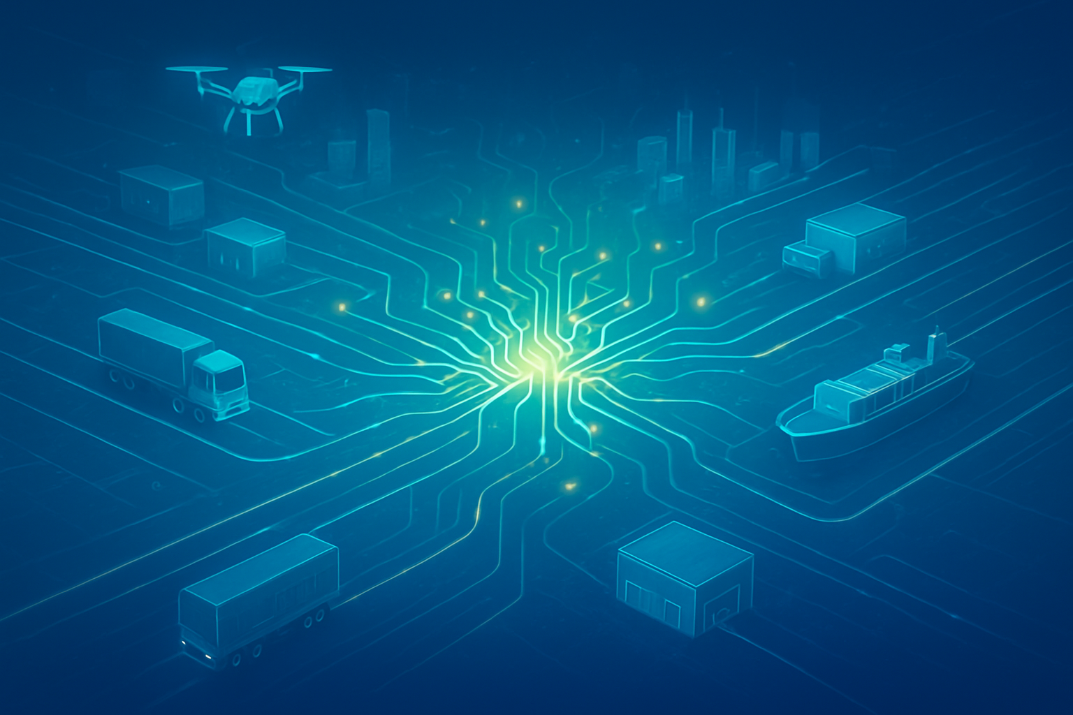
The strategic technological shift towards tech stack consolidation involves streamlining an organization's technology infrastructure by reducing the number of standalone software tools and platforms. At its core, this entails establishing a single source of truth for all logistics data, eliminating silos, and improving data accuracy and consistency. This move facilitates standardized communication and processes across partner networks, moving beyond outdated methods like manual data entry and email-based coordination.
Modern consolidated logistics tech stacks typically revolve around the seamless integration of several core platforms. Enterprise Resource Planning (ERP) systems often serve as the central backbone, unifying core business processes from accounting to procurement. Warehouse Management Systems (WMS) optimize inventory tracking, storage, picking, and packing, while Transportation Management Systems (TMS) streamline route optimization, carrier management, and real-time shipment tracking. Order Management Systems (OMS) coordinate the entire order lifecycle, from capture to fulfillment. Beyond these, specialized tools for route optimization, delivery management, mobile driver applications, and advanced analytics are being integrated.
This consolidated approach fundamentally differs from the previous fragmented technology adoption. Historically, departments often adopted specialized software that struggled to communicate, leading to manual processes and redundant data entry. Integration was complex, costly, and often relied on slower, batch-based Electronic Data Interchange (EDI). In contrast, modern consolidated systems leverage modular, cloud-native architectures, often utilizing platforms from tech giants like Amazon Web Services (AWS), Microsoft Azure (MSFT), or Google Cloud Platform (GOOGL). They rely heavily on robust RESTful APIs (Application Programming Interfaces) for real-time, bidirectional communication, often supported by middleware and integration platforms or message queuing systems like Apache Kafka. The data architecture prioritizes a unified data platform with canonical data models and central data warehouses/lakes, enabling real-time analytics and comprehensive reporting.
Logistics and supply chain experts largely view this consolidation as a critical and necessary trend. They emphasize its importance for resilience and adaptability, highlighting real-time visibility as a "game-changer." While acknowledging challenges like integration complexity with legacy systems and the need for effective change management, experts believe this trend "massively decreases" the lift for shippers to adopt new technology, accelerating a "tech-driven future" with increased investments in AI and automation.
Competitive Implications and Market Dynamics
The trend of shippers consolidating their tech stacks is profoundly reshaping the competitive landscape across the logistics and supply chain sector, creating both immense opportunities and significant challenges for various players.
AI companies are uniquely positioned to benefit. Consolidated tech stacks, by providing clean, centralized data, offer fertile ground for advanced AI capabilities in areas such as predictive demand forecasting, route optimization, network planning, and automation across warehousing and transportation. AI is becoming an integral component of future logistics software, with rapid technological advancements making it more accessible and cost-effective. Companies specializing in AI for real-time tracking, cargo monitoring, and predictive analytics stand to gain immensely.
Tech giants, with their extensive R&D budgets and vast ecosystems, are making strategic moves through acquisitions, partnerships, and substantial investments. Their ability to seamlessly integrate digital logistics solutions with broader enterprise software portfolios—including ERP, CRM, and Business Intelligence (BI) solutions—offers a comprehensive ecosystem to shippers. Companies like Amazon (AMZN), Google (GOOGL), and Salesforce (CRM) are actively expanding their footprint in supply chain technology, leveraging their scale and cloud infrastructure.
For startups, the consolidated landscape presents a mixed bag. Innovative freight tech startups, particularly those focused on AI, automation, sustainability, or niche solutions, are becoming attractive acquisition targets for larger, traditional logistics firms or tech giants seeking to rapidly innovate. Startups developing universal APIs that simplify connectivity between diverse WMS and other logistics platforms are also uniquely positioned to thrive, as integration complexity remains a major hurdle for shippers. However, startups face challenges such as high implementation costs, compatibility issues with existing legacy systems, and the need to address skill gaps within client organizations.
Companies offering comprehensive, end-to-end logistics platforms that integrate various functions (TMS, WMS, OMS, SCP) into a single system are poised to benefit most. Cloud service providers (e.g., AWS, Azure) will also see continued growth as modern tech stacks increasingly migrate to the cloud. The competitive landscape will intensify, with major AI labs and tech companies vying for market dominance by developing comprehensive suites, focusing on seamless data integration, and engaging in strategic mergers and acquisitions. Fragmented point solutions and legacy systems that lack robust integration capabilities face significant disruption and potential obsolescence as shippers favor unified platforms.
The Broader Significance: AI's Role in a Connected Supply Chain
The consolidation of tech stacks by shippers is a development of wider significance, deeply intertwined with the broader AI landscape and current technological trends. In an era where data is paramount, a unified tech stack provides the foundational infrastructure necessary to effectively leverage advanced analytics and AI capabilities.
This trend perfectly aligns with the current AI revolution. Consolidated platforms act as a single source of truth, feeding AI and ML algorithms with the comprehensive, clean data required for accurate demand forecasting, route optimization, predictive maintenance, and anomaly detection. Cloud computing is central, offering scalability and flexibility for processing vast amounts of data. The integration of IoT devices provides real-time tracking, while AI-driven automation in warehouses and digital twin technology for supply chain simulation are transforming operations. The advent of 5G connectivity further enables real-time logistics through low latency and high data transmission, crucial for integrated systems.
The overall impacts on the supply chain are profound: enhanced efficiency and cost reduction through automation and optimized routes; improved visibility and transparency from end-to-end tracking; increased resilience and adaptability through predictive analytics; better decision-making from clean, centralized data; and an enhanced customer experience. Furthermore, technology-driven supply chains contribute to sustainability by optimizing routes and reducing waste.
However, potential concerns include vendor lock-in, where reliance on a single provider can limit flexibility and innovation. Data privacy and security risks are also heightened with centralized data, making robust cybersecurity essential. Integrating existing legacy systems with new unified platforms remains a complex and expensive challenge. High initial investment, particularly for small and medium-sized enterprises (SMEs), can also be a barrier.
Comparing this to previous technological shifts in logistics, such as containerization in the 1960s or the advent of GPS tracking in the 2000s, the current AI-driven tech consolidation represents a "supercycle." While past shifts focused on mechanization, digitization, and basic connectivity, today's shift leverages AI, machine learning, and advanced data analytics to create interconnected, predictive, and adaptive supply chains, fundamentally redefining efficiency and strategic planning. The move is towards true intelligence, autonomy, and predictive capabilities across the entire supply chain, marking a significant milestone in logistics technology.
The Horizon: Future Developments in Logistics Tech
The path forward for logistics tech consolidation is paved with exciting near-term and long-term developments, promising to reshape the industry profoundly.
In the near term (2024-2025), expect a more prominent integration of AI and automation for predictive analytics in demand forecasting, inventory management, and order processing. Enhanced collaboration and the dominance of digital supply chains, leveraging technologies like blockchain and IoT for transparency and traceability, will become standard. The logistics tech landscape will likely see increased mergers and acquisitions (M&A) as companies seek to expand capabilities and modernize their tech stacks, with TMS providers integrating smaller, specialized technologies. A growing focus on sustainability will also drive the adoption of eco-friendly practices and technologies.
Looking further ahead (2026 and beyond), Gartner predicts that by 2027, 80% of manufacturing operations management solutions will be cloud-native and edge-driven, bridging the IT/OT convergence gap. By 2028, smart robots are expected to outnumber frontline workers in manufacturing, retail, and logistics, driven by labor shortages. Generative AI is anticipated to power 25% of supply chain KPI reporting, enhancing decision-making speed and quality. The emergence of Decision Intelligence Technology, leveraging advanced algorithms and machine learning, will dramatically optimize decision-making flows in real-time.
Potential applications and use cases on the horizon include AI-driven demand forecasting and scenario planning, leveraging digital twins to simulate operations. Real-time tracking and enhanced visibility will become ubiquitous, while AI will optimize transportation management, including dynamic rerouting and shared truckload models. Automated warehouse operations using AI-powered robots will streamline fulfillment. Last-mile delivery will see innovations like autonomous vehicles and smart lockers. AI systems will also enhance risk management and predictive maintenance, flagging potential security breaches and predicting equipment failures. Digital freight matching platforms will transform brokerage, and customer experience will be further improved through AI-driven communication.
However, several challenges need to be addressed. High implementation costs and the complexity of integrating with legacy systems remain significant hurdles. Employee and management pushback, stemming from fears of job displacement or perceived complexity, can impede adoption. Data security risks, complex coordination, cost allocation issues in consolidated freight, and ensuring scalability for growth are also critical. Many companies still lack the in-house resources and expertise to build and maintain advanced tech stacks.
Experts predict that technology adoption is no longer optional but a necessity for companies to navigate market volatility. Upskilling the workforce will be crucial, and M&A activity will continue, with carriers strategically acquiring companies to realign portfolios towards specialized, high-margin areas. Shifting service models, including crowd-sharing delivery models and large companies transforming internal logistics into standalone businesses, are also anticipated. Ultimately, the focus on innovation, collaboration, and sustainability is expected to lead to enhanced resilience and efficiency, stabilizing the sector amidst global uncertainties.
A New Era of Intelligent Logistics
The consolidation of tech stacks by shippers marks a pivotal moment in the evolution of the logistics and supply chain industry. It represents a fundamental strategic reorientation, moving away from reactive, fragmented technology adoption towards a proactive, integrated, and intelligent approach.
The key takeaway is that this shift is not merely a technological upgrade but a commitment to leveraging interconnected systems and advanced analytics, particularly AI, to build more intelligent, adaptive, and customer-centric supply chains for the future. The benefits are clear: significant improvements in operational efficiency, substantial cost reductions, unparalleled data visibility, and enhanced resilience against market disruptions. AI, in particular, stands as a central pillar, transforming everything from predictive forecasting and route optimization to warehouse automation and customer service.
This development holds immense significance in AI history within the logistics domain. Unlike previous phases where AI was often a theoretical concept or in nascent pilot stages, it has now transitioned into a practical, pervasive tool. This consolidation provides the necessary infrastructure for AI to move beyond isolated applications to deeply embedded, autonomous decision-making systems across the entire supply chain. It signifies a maturation of digital transformation, where technology is no longer just an enabler but a core strategic asset and a growth engine.
In the long term, this trend will lead to fundamentally more resilient, efficient, and sustainable supply chains. Companies that successfully embrace this transformation will gain a significant competitive edge, while those that cling to fragmented legacy systems risk falling behind in an increasingly data-driven and automated world. The industry will likely see continued M&A activity among technology providers, driven by the demand for comprehensive, scalable solutions.
In the coming weeks and months, watch for continued M&A activity, accelerated adoption of advanced AI and automation (including generative AI), and emerging best practices in seamless integration and data governance. Pay close attention to sustainability-driven tech investments, the expanding role of 5G and blockchain, and how evolving partner ecosystems adapt to this new era of integrated logistics. The great unification of logistics tech stacks is underway, promising a future of unprecedented efficiency and intelligence.
This content is intended for informational purposes only and represents analysis of current AI developments.
TokenRing AI delivers enterprise-grade solutions for multi-agent AI workflow orchestration, AI-powered development tools, and seamless remote collaboration platforms.
For more information, visit https://www.tokenring.ai/.