The artificial intelligence landscape is undergoing a profound transformation, moving away from the sole pursuit of increasingly massive AI models towards the development and deployment of smaller, more efficient, and specialized solutions. This emerging trend, dubbed the "small models, big shift," signifies a pivotal moment in AI history, challenging the long-held belief that "bigger is always better." It promises to democratize access to advanced AI capabilities, accelerate innovation, and pave the way for more sustainable and practical applications across industries.
This shift is driven by a growing recognition of the inherent limitations and exorbitant costs associated with colossal models, coupled with the remarkable capabilities demonstrated by their more compact counterparts. By prioritizing efficiency, accessibility, and task-specific optimization, small AI models are set to redefine how AI is developed, deployed, and integrated into our daily lives and enterprise operations.
The Technical Underpinnings of a Leaner AI Future
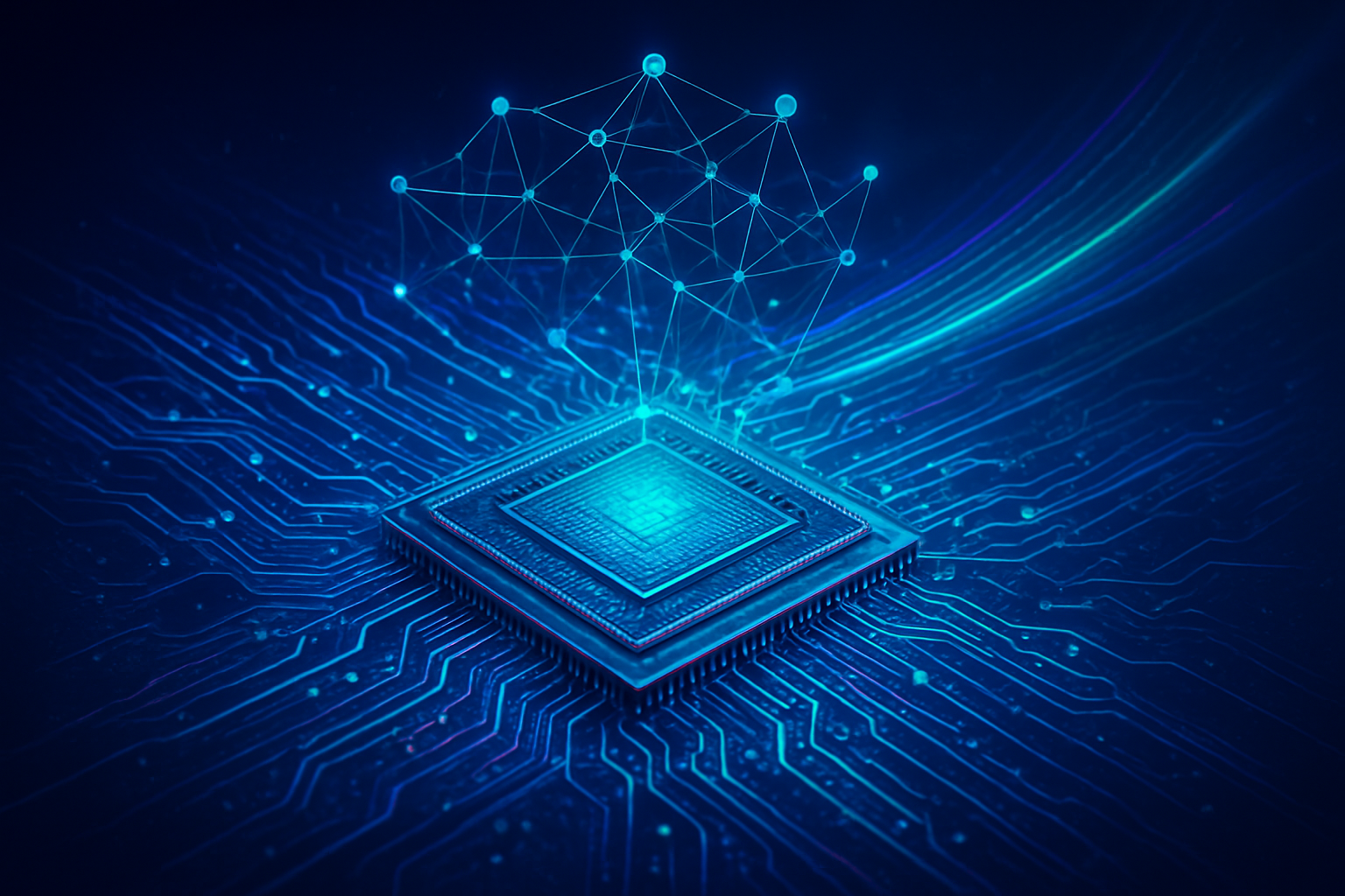
The "small models, big shift" is rooted in significant technical advancements that enable AI models to achieve high performance with a fraction of the parameters and computational resources of their predecessors. These smaller models, often referred to as Small Language Models (SLMs) or "tiny AI," typically range from a few million to approximately 10 billion parameters, a stark contrast to the hundreds of billions or even trillions seen in Large Language Models (LLMs) like GPT-4.
Technically, SLMs leverage optimized architectures and sophisticated training techniques. Many employ simplified transformer architectures, enhanced with innovations like sparse attention mechanisms (e.g., sliding-window attention in Microsoft's (NASDAQ: MSFT) Phi-3 series) and parameter sharing to reduce computational overhead. A cornerstone for creating efficient SLMs is knowledge distillation, where a smaller "student" model is trained to mimic the outputs and internal features of a larger, more complex "teacher" model. This allows the student model to generalize effectively with fewer parameters. Other techniques include pruning (removing redundant connections) and quantization (reducing the precision of numerical values, e.g., from 32-bit to 4-bit, to significantly cut memory and computational requirements). Crucially, SLMs often benefit from highly curated, "textbook-quality" synthetic data, which boosts their reasoning skills without inflating their parameter count.
These technical differences translate into profound practical advantages. SLMs require significantly less computational power, memory, and energy, enabling them to run efficiently on consumer-grade hardware, mobile devices, and even microcontrollers, eliminating the need for expensive GPUs and large-scale cloud infrastructure for many tasks. This contrasts sharply with LLMs, which demand immense computational resources and energy for both training and inference, leading to high operational costs and a larger carbon footprint. While LLMs excel in complex, open-ended reasoning and broad knowledge, SLMs often deliver comparable or even superior performance for specific, domain-specific tasks, thanks to their specialized training. The AI research community and industry experts have largely welcomed this trend, citing the economic benefits, the democratization of AI, and the potential for ubiquitous edge AI deployment as major advantages. NVIDIA (NASDAQ: NVDA) research, for instance, has explicitly challenged the "bigger is always better" assumption, suggesting SLMs can handle a significant portion of AI agent tasks without performance compromise, leading to substantial cost savings.
Reshaping the AI Competitive Landscape
The "small models, big shift" is profoundly reshaping the competitive dynamics for AI companies, tech giants, and startups alike, fostering a new era of innovation and accessibility. This trend is driven by the realization that "right-sizing AI" – aligning model capabilities with specific business needs – often yields better results than simply chasing scale.
Tech giants, while historically leading the charge in developing massive LLMs, are actively embracing this trend. Companies like Google (NASDAQ: GOOGL) with its Gemma family, Microsoft (NASDAQ: MSFT) with its Phi series, and IBM (NYSE: IBM) with its Granite Nano models are all developing and releasing compact versions of their powerful AI. This allows them to expand market reach by offering more affordable and accessible AI solutions to small and medium-sized enterprises (SMEs), optimize existing services with efficient, specialized AI for improved performance and reduced latency, and address specific enterprise use cases requiring speed, privacy, and compliance through edge deployment or private clouds.
However, the trend is particularly advantageous for AI startups and smaller businesses. It drastically lowers the financial and technical barriers to entry, enabling them to innovate and compete without the massive capital investments traditionally required for AI development. Startups can leverage open-source frameworks and cloud-based services with smaller models, significantly reducing infrastructure and training costs. This allows them to achieve faster time to market, focus on niche specialization, and build competitive advantages by developing highly tailored solutions that might outperform larger general-purpose models in specific domains. Companies specializing in specific industries, like AiHello in Amazon advertising, are already demonstrating significant growth and profitability by adopting this "domain-first AI" approach. The competitive landscape is shifting from who can build the largest model to who can build the most effective, specialized, and efficient model for a given task, democratizing AI innovation and making operational excellence a key differentiator.
A Broader Significance: AI's Maturing Phase
The "small models, big shift" represents a crucial redirection within the broader AI landscape, signaling a maturing phase for the industry. It aligns with several key trends, including the democratization of AI, the expansion of Edge AI and the Internet of Things (IoT), and a growing emphasis on resource efficiency and sustainability. This pivot challenges the "bigger is always better" paradigm that characterized the initial LLM boom, recognizing that for many practical applications, specialized, efficient, and affordable smaller models offer a more sustainable and impactful path.
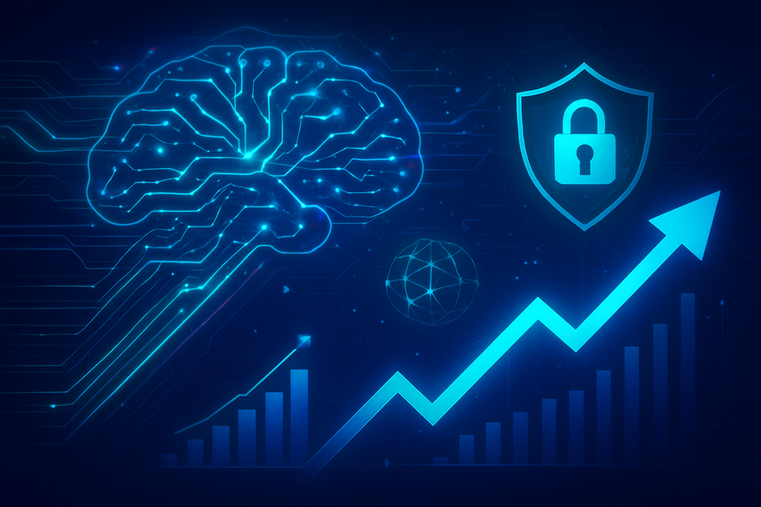
The impacts are wide-ranging. Positively, it drives down costs, accelerates processing times, and enhances accessibility, fostering innovation from a more diverse community. It also improves privacy and security by enabling local processing of sensitive data and contributes to environmental sustainability through reduced energy consumption. However, potential concerns loom. Small models may struggle with highly complex or nuanced tasks outside their specialization, and their performance is heavily dependent on high-quality, relevant data, with a risk of overfitting. A significant concern is model collapse, a phenomenon where AI models trained on increasingly synthetic, AI-generated data can degrade in quality over time, leading to a loss of originality, amplification of biases, and ultimately, the production of unreliable or nonsensical outputs. This risk is exacerbated by the widespread proliferation of AI-generated content, potentially diminishing the pool of pure human-generated data for future training.
Comparing this to previous AI milestones, the current shift moves beyond the early AI efforts constrained by computational power, the brittle expert systems of the 1980s, and even the "arms race" for massive deep learning models and LLMs of the late 2010s. While the release of OpenAI's (private) GPT-3 in 2020 marked a landmark moment for general intelligence, the "small models, big shift" acknowledges that for most real-world applications, a "fit-for-purpose" approach with efficient, specialized models offers a more practical and sustainable future. It envisions an ecosystem where both massive foundational models and numerous specialized smaller models coexist, each optimized for different purposes, leading to more pervasive, practical, and accessible AI solutions.
The Horizon: Ubiquitous, Adaptive, and Agentic AI
Looking ahead, the "small models, big shift" is poised to drive transformative developments in AI, leading to more ubiquitous, adaptive, and intelligent systems. In the near term (next 1-3 years), we can expect continued advancements in optimization techniques like 4-bit quantization, drastically reducing model size with minimal accuracy trade-offs. The proliferation of specialized chips (e.g., Apple's Neural Engine, Qualcomm (NASDAQ: QCOM) Hexagon, Google (NASDAQ: GOOGL) Tensor) will accelerate on-device AI, enabling models like Microsoft's (NASDAQ: MSFT) Phi-3 Mini to demonstrate performance comparable to larger models on specific reasoning, math, and coding tasks. Hybrid AI architectures, combining local models with cloud fallback and vector memory, will become more prevalent, allowing for personalized, immediate, and context-aware interactions.
In the long term (next 5-10 years), small AI models are expected to power truly "invisible AI" integrated into our daily lives. This includes phones summarizing emails offline, smart glasses translating signs in real-time, and personal AI assistants running entirely on local hardware. The emphasis will move beyond merely running pre-trained models to enabling on-device learning and adaptation, improving privacy as data remains local. Experts foresee a future dominated by agentic AI systems, where networks of smaller, specialized models are orchestrated to solve complex sub-tasks, offering superior cost, latency, robustness, and maintainability for decomposable problems. Potential applications span smart devices in IoT, industrial automation, agriculture, healthcare (e.g., patient monitoring with local data), finance (on-premise fraud detection), and enhanced mobile experiences with private, offline AI.
However, challenges remain. Small models may still struggle with highly complex language comprehension or open-ended creative tasks. The development complexity of distillation and quantization techniques requires specialized expertise. Ensuring high-quality data to avoid overfitting and bias, especially in sensitive applications, is paramount. Moreover, the sheer volume of new AI-generated content poses a threat of "model collapse" if future models are trained predominantly on synthetic data. Experts like Igor Izraylevych, CEO of S-PRO, predict that "the future of AI apps won't be decided in the cloud. It will be decided in your pocket," underscoring the shift towards personalized, on-device intelligence. ABI Research estimates approximately 2.5 billion TinyML devices globally by 2030, generating over US$70 billion in economic value, highlighting the immense market potential.
A New Chapter for AI: Efficiency as the North Star
The "small models, big shift" represents a pivotal moment in artificial intelligence, moving beyond the era of brute-force computation to one where intelligent design, efficiency, and widespread applicability are paramount. The key takeaways are clear: AI is becoming more cost-effective, accessible, specialized, and privacy-preserving. This shift is democratizing innovation, enabling a broader array of developers and businesses to harness the power of AI without prohibitive costs or computational demands.
Its significance in AI history cannot be overstated. It marks a maturation of the field, demonstrating that optimal performance often comes not from sheer scale, but from tailored efficiency. This new paradigm will lead to a future where AI is deeply embedded in our daily lives, from edge devices to enterprise solutions, all operating with unprecedented speed and precision. The long-term impact promises accelerated innovation, widespread AI integration, and a more sustainable technological footprint, though it will also necessitate significant investments in workforce upskilling and robust ethical governance frameworks.
In the coming weeks and months, watch for continued advancements in model compression techniques, a proliferation of open-source small models from major players and the community, and increased enterprise adoption in niche areas. Expect to see further hardware innovation for edge AI and the development of sophisticated frameworks for orchestrating multiple specialized AI agents. Ultimately, the "small models, big shift" signals that the future of AI is not solely about building the biggest brain, but about creating a vast, intelligent ecosystem of specialized, efficient, and impactful solutions that are accessible to all.
This content is intended for informational purposes only and represents analysis of current AI developments.
TokenRing AI delivers enterprise-grade solutions for multi-agent AI workflow orchestration, AI-powered development tools, and seamless remote collaboration platforms.
For more information, visit https://www.tokenring.ai/.