In a move that has sent shockwaves through the global technology sector, Taiwan Semiconductor Manufacturing Company (NYSE: TSM) officially announced on January 15, 2026, a historic capital expenditure budget of $52 billion to $56 billion for the 2026 fiscal year. This unprecedented financial commitment, representing a nearly 40% increase over the previous year, is designed to aggressively scale the world’s first 2-nanometer (2nm) and 1.6-nanometer (A16) production lines. The announcement marks the definitive start of what CEO C.C. Wei described as the "AI Giga-cycle," a period of structural, non-cyclical demand for high-performance computing (HPC) that is fundamentally reshaping the semiconductor industry.
The sheer scale of this investment underscores TSMC’s role as the indispensable foundation of the modern AI economy. With nearly 80% of the budget dedicated to advanced process technologies and another 20% earmarked for advanced packaging solutions like CoWoS (Chip on Wafer on Substrate), the company is positioning itself to meet the "insatiable" demand for compute power from hyperscalers and sovereign nations alike. Industry analysts suggest that this capital injection effectively creates a multi-year "strategic moat," making it increasingly difficult for competitors to bridge the widening gap in leading-edge manufacturing capacity.
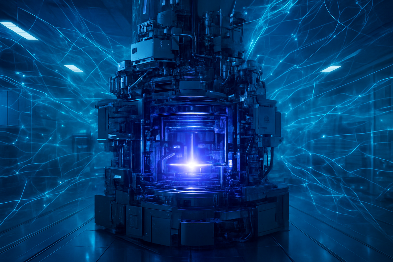
The Angstrom Era: 2nm Nanosheets and the A16 Revolution
The technical centerpiece of TSMC’s 2026 expansion is the rapid ramp-up of the N2 (2nm) family and the introduction of the A16 (1.6nm) node. Unlike the FinFET architecture used in previous generations, the 2nm node utilizes Gate-All-Around (GAA) nanosheet transistors. This transition allows for superior electrostatic control, significantly reducing power leakage while boosting performance. Initial reports indicate that TSMC has achieved production yields of 65% to 75% for its 2nm process, a figure that is reportedly years ahead of its primary rivals, Intel (NASDAQ: INTC) and Samsung (KRX: 005930).
Even more anticipated is the A16 node, slated for volume production in the second half of 2026. A16 represents the dawn of the "Angstrom Era," introducing TSMC’s proprietary "Super Power Rail" (SPR) technology. SPR is a form of backside power delivery that moves the power routing to the back of the silicon wafer. This architectural shift eliminates the competition for space between power lines and signal lines on the front side, drastically reducing voltage drops and allowing for an 8% to 10% speed improvement and a 15% to 20% power reduction compared to the N2P process.
This technical leap is not just an incremental improvement; it is a total redesign of how chips are powered. By decoupling power and signal delivery, TSMC is enabling the creation of denser, more efficient AI accelerators that can handle the massive parameters of next-generation Large Language Models (LLMs). Initial reactions from the AI research community have been electric, with experts noting that the efficiency gains of A16 will be critical for maintaining the sustainability of massive AI data centers, which are currently facing severe energy constraints.
Powering the Titans: How the Giga-cycle Reshapes Big Tech
The implications of TSMC’s massive investment extend directly to the balance of power among tech giants. NVIDIA (NASDAQ: NVDA) and Apple (NASDAQ: AAPL) have already emerged as the primary beneficiaries, with reports suggesting that Apple has secured the majority of early 2nm capacity for its upcoming A20 and M6 series processors. Meanwhile, NVIDIA is rumored to be the lead customer for the A16 node to power its post-Blackwell "Feynman" GPU architecture, ensuring its dominance in the AI accelerator market remains unchallenged.
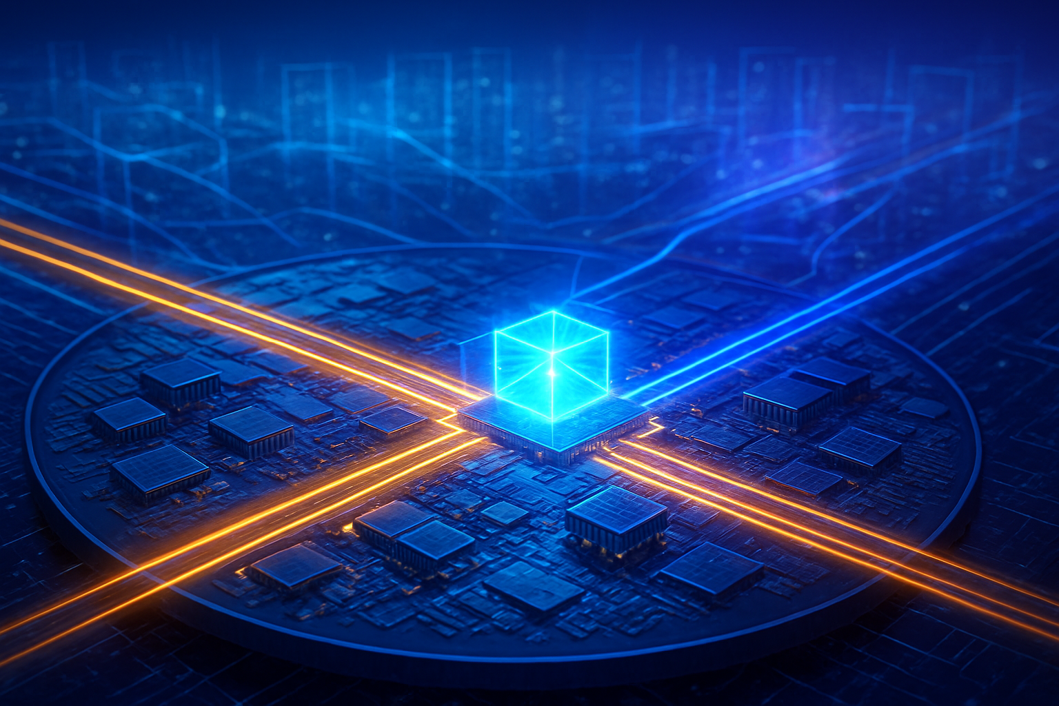
For hyperscalers like Microsoft (NASDAQ: MSFT), Meta (NASDAQ: META), and Alphabet (NASDAQ: GOOGL), TSMC’s Capex surge provides the physical infrastructure necessary to realize their aggressive AI roadmaps. These companies are increasingly moving toward custom silicon—designing their own AI chips to reduce reliance on off-the-shelf components. TSMC’s commitment to advanced packaging is the "secret sauce" here; without the ability to package these massive chips using CoWoS or SoIC (System on Integrated Chips) technology, the raw wafers would be unusable for high-end AI applications.
The competitive landscape for startups and smaller AI labs is more complex. While the increased capacity may eventually lead to better availability of compute resources, the "front-loading" of orders by tech titans could keep leading-edge nodes out of reach for smaller players for several years. This has led to a strategic shift where many startups are focusing on software optimization and "small model" efficiency, even as the hardware giants double down on the massive scale of the Giga-cycle.
A New Global Landscape: Sovereign AI and the Silicon Shield
Beyond the balance sheets of Silicon Valley, TSMC’s 2026 budget reflects a profound shift in the broader AI landscape. One of the most significant drivers identified in this cycle is "Sovereign AI." Nation-states are no longer content to rely on foreign cloud providers for their compute needs; they are now investing billions to build domestic AI clusters as a matter of national security and economic independence. This new tier of customers is contributing to a "floor" in demand that protects TSMC from the traditional boom-and-bust cycles of the semiconductor industry.
Geopolitical resiliency is also a core component of this spending. A significant portion of the $56 billion budget is earmarked for TSMC’s "Gigafab" expansion in Arizona. With Fab 1 already in high-volume manufacturing and Fab 2 slated for tool-in during 2026, TSMC is effectively building a "Silicon Shield" for the United States. For the first time, the company has also confirmed plans to establish advanced packaging facilities on U.S. soil, addressing a major vulnerability in the AI supply chain where chips were previously manufactured in the U.S. but had to be sent back to Asia for final assembly.
This massive capital infusion also acts as a catalyst for the broader supply chain. Shares of equipment manufacturers like ASML (NASDAQ: ASML), Applied Materials (NASDAQ: AMAT), and Lam Research (NASDAQ: LRCX) have reached all-time highs as they prepare for a flood of orders for High-NA EUV lithography machines and specialized deposition tools. The investment signal from TSMC effectively confirms that the "AI bubble" concerns of 2024 and 2025 were premature; the infrastructure phase of the AI era is only just reaching its peak.
The Road Ahead: Overcoming the Scaling Wall
Looking toward 2027 and beyond, TSMC is already eyeing the N2P and N2X iterations of its 2nm node, as well as the transition to 1.4nm (A14) technology. The near-term focus will be on the seamless integration of backside power delivery across all leading-edge nodes. However, significant challenges remain. The primary hurdle is no longer just transistor density, but the "energy wall"—the difficulty of delivering enough power to these ultra-dense chips and cooling them effectively.
Experts predict that the next two years will see a massive surge in "3D Integrated Circuits" (3D IC), where logic and memory are stacked directly on top of each other. TSMC’s SoIC technology will be pivotal here, allowing for much higher bandwidth and lower latency than traditional packaging. The challenge for TSMC will be managing the sheer complexity of these designs while maintaining the high yields that its customers have come to expect.
In the long term, the industry is watching for how TSMC balances its global expansion with the rising costs of electricity and labor. The Arizona and Japan expansions are expensive ventures, and maintaining the company’s industry-leading margins while spending $56 billion a year will require flawless execution. Nevertheless, the trajectory is clear: TSMC is betting that the AI Giga-cycle is the most significant economic transformation since the industrial revolution, and they are building the engine to power it.
Conclusion: A Definitive Moment in AI History
TSMC’s $56 billion capital expenditure plan for 2026 is more than just a financial forecast; it is a declaration of confidence in the future of artificial intelligence. By committing to the rapid scaling of 2nm and A16 technologies, TSMC has effectively set the pace for the entire technology industry. The takeaways are clear: the AI Giga-cycle is real, it is physical, and it is being built in the cleanrooms of Hsinchu, Kaohsiung, and Phoenix.
As we move through 2026, the industry will be closely watching the tool-in progress at TSMC’s global sites and the initial performance metrics of the first A16 test chips. This development represents a pivotal moment in AI history—the point where the theoretical potential of generative AI meets the massive, tangible infrastructure required to support it. For the coming weeks and months, the focus will shift to how competitors like Intel and Samsung respond to this massive escalation, and whether they can prevent a total TSMC monopoly on the Angstrom era.
This content is intended for informational purposes only and represents analysis of current AI developments.
TokenRing AI delivers enterprise-grade solutions for multi-agent AI workflow orchestration, AI-powered development tools, and seamless remote collaboration platforms.
For more information, visit https://www.tokenring.ai/.