The semiconductor industry is currently navigating a period of unprecedented dynamism, marked by robust growth, groundbreaking technological advancements, and a palpable shift in investor focus. As the foundational bedrock of the modern digital economy, semiconductors are at the heart of every major innovation, from artificial intelligence to electric vehicles. This strategic importance has made the sector a magnet for significant capital, with investors keenly observing companies that are not only driving this technological evolution but also demonstrating resilience and profitability in a complex global landscape. A prime example of this investor confidence recently manifested in ON Semiconductor's (NASDAQ: ON) strong third-quarter 2025 financial results, which provided a positive jolt to market sentiment and underscored the sector's compelling investment narrative.
The global semiconductor market is on a trajectory to reach approximately $697 billion in 2025, an impressive 11% year-over-year increase, with ambitious forecasts predicting a potential $1 trillion valuation by 2030. This growth is not uniform, however, with specific segments emerging as critical areas of investor interest due to their foundational role in the next wave of technological advancement. The confluence of AI proliferation, the electrification of the automotive industry, and strategic government initiatives is reshaping the investment landscape within semiconductors, signaling a pivotal era for the industry.
The Microchip's Macro Impact: Dissecting Key Investment Hotbeds and Technical Leaps
The current investment fervor in the semiconductor sector is largely concentrated around several high-growth, technologically intensive domains. Artificial Intelligence (AI) and High-Performance Computing (HPC) stand out as the undisputed leaders, with demand for generative AI chips alone projected to exceed $150 billion in 2025. This encompasses a broad spectrum of components, including advanced CPUs, GPUs, data center communication chips, and high-bandwidth memory (HBM). Companies like Nvidia (NASDAQ: NVDA), Broadcom (NASDAQ: AVGO), and TSMC (NYSE: TSM) are at the vanguard of this AI-driven surge, as data center markets, particularly for GPUs and advanced storage, are expected to grow at an 18% Compound Annual Growth Rate (CAGR), potentially reaching $361 billion by 2030.
Beyond AI, the automotive sector presents another significant growth avenue, despite a slight slowdown in late 2024. The relentless march towards electric vehicles (EVs), advanced driver-assistance systems (ADAS), and sophisticated energy storage solutions means that EVs now utilize two to three times more chips than their traditional internal combustion engine counterparts. This drives immense demand for power management, charging infrastructure, and energy efficiency solutions, with the EV semiconductor devices market alone forecasted to expand at a remarkable 30% CAGR from 2025 to 2030. Memory technologies, especially HBM, are also experiencing a resurgence, fueled by AI accelerators and cloud computing, with HBM growing 200% in 2024 and an anticipated 70% increase in 2025. The SSD market is also on a robust growth path, projected to hit $77 billion by 2025.
What distinguishes this current wave of innovation from previous cycles is the intense focus on advanced packaging and manufacturing technologies. Innovations such as 3D stacking, chiplets, and technologies like CoWoS (chip-on-wafer-on-substrate) are becoming indispensable for achieving the efficiency and performance levels required by modern AI chips. Furthermore, the industry is pushing the boundaries of process technology with the development of 2-nm Gate-All-Around (GAA) chips, promising unprecedented levels of performance and energy efficiency. These advancements represent a significant departure from traditional monolithic chip designs, enabling greater integration, reduced power consumption, and enhanced processing capabilities crucial for demanding AI and HPC applications. The initial market reactions, such as the positive bump in ON Semiconductor's stock following its earnings beat, underscore investor confidence in companies that demonstrate strong execution and strategic alignment with these high-growth segments, even amidst broader market challenges. The company's focus on profitability and strategic pivot towards EVs, ADAS, industrial automation, and AI applications, despite a projected decline in silicon carbide revenue in 2025, highlights a proactive adaptation to evolving market demands.
The AI Supercycle's Ripple Effect: Shaping Corporate Fortunes and Competitive Battlegrounds
The current surge in semiconductor investment, propelled by an insatiable demand for artificial intelligence capabilities and bolstered by strategic government initiatives, is dramatically reshaping the competitive landscape for AI companies, tech giants, and nascent startups alike. This "AI Supercycle" is not merely driving growth; it is fundamentally altering market dynamics, creating clear beneficiaries, intensifying rivalries, and forcing strategic repositioning across the tech ecosystem.
At the forefront of this transformation are the AI chip designers and manufacturers. NVIDIA (NASDAQ: NVDA) continues to dominate the AI GPU market with its Hopper and Blackwell architectures, benefiting from unprecedented orders and a comprehensive full-stack approach that integrates hardware and software. However, competitors like Advanced Micro Devices (NASDAQ: AMD) are rapidly gaining ground with their MI series accelerators, directly challenging NVIDIA's hegemony in the high-growth AI server market. Taiwan Semiconductor Manufacturing Company (NYSE: TSM), as the world's leading foundry, is experiencing overwhelming demand for its cutting-edge process nodes and advanced packaging technologies like Chip-on-Wafer-on-Substrate (CoWoS), projecting a remarkable 40% compound annual growth rate for its AI-related revenue through 2029. Broadcom (NASDAQ: AVGO) is also a strong player in custom AI processors and networking solutions critical for AI data centers. Even Intel (NASDAQ: INTC) is aggressively pushing its foundry services and AI chip portfolio, including Gaudi accelerators and pioneering neuromorphic computing with its Loihi chips, to regain market share and position itself as a comprehensive AI provider.
Major tech giants, often referred to as "hyperscalers" such as Microsoft (NASDAQ: MSFT), Alphabet (NASDAQ: GOOGL), Amazon (NASDAQ: AMZN), Meta (NASDAQ: META), and Oracle (NYSE: ORCL), are not just massive consumers of these advanced chips; they are increasingly designing their own custom AI silicon (ASICs and TPUs). This vertical integration strategy allows them to optimize performance for their specific AI workloads, control costs, and reduce reliance on external suppliers. This move presents a significant competitive threat to pure-play chip manufacturers, as these tech giants internalize a substantial portion of their AI hardware needs. For AI startups, while the availability of advanced hardware is increasing, access to the highest-end chips can be a bottleneck, especially without the purchasing power or strategic partnerships of larger players. This can lead to situations, as seen with some Chinese AI companies impacted by export bans, where they must consume significantly more power to achieve comparable results.
The ripple effect extends to memory manufacturers like Micron Technology (NASDAQ: MU) and Samsung Electronics (KRX: 005930), who are heavily investing in High Bandwidth Memory (HBM) production to meet the memory-intensive demands of AI workloads. Semiconductor equipment suppliers, such as Lam Research (NASDAQ: LRCX), are also significant beneficiaries as foundries and chipmakers pour capital into new equipment for leading-edge technologies. Furthermore, companies like ON Semiconductor (NASDAQ: ON) are critical for providing the high-efficiency power management solutions essential for supporting the escalating compute capacity in AI data centers, highlighting their strategic value in the evolving ecosystem. The "AI Supercycle" is also driving a major PC refresh cycle, as demand for AI-capable devices with Neural Processing Units (NPUs) increases. This era is defined by a shift from traditional CPU-centric computing to heterogeneous architectures, fundamentally disrupting existing product lines and necessitating massive investments in new R&D across the board.
Beyond the Silicon Frontier: Wider Implications and Geopolitical Fault Lines
The unprecedented investment in the semiconductor sector, largely orchestrated by the advent of the "AI Supercycle," represents far more than just a technological acceleration; it signifies a profound reshaping of economic landscapes, geopolitical power dynamics, and societal challenges. This era distinguishes itself from previous technological revolutions by the symbiotic relationship between AI and its foundational hardware, where AI not only drives demand for advanced chips but also actively optimizes their design and manufacturing.
Economically, the impact is immense, with projections placing the global semiconductor industry at $800 billion in 2025, potentially surging past $1 trillion by 2028. This growth fuels aggressive research and development, rapidly advancing AI capabilities across diverse sectors from healthcare and finance to manufacturing and autonomous systems. Experts frequently liken this "AI Supercycle" to transformative periods like the advent of personal computers, the internet, mobile, and cloud computing, suggesting a new, sustained investment cycle. However, a notable distinction in this cycle is the heightened concentration of economic profit among a select few top-tier companies, which generate the vast majority of the industry's economic value.
Despite the immense opportunities, several significant concerns cast a shadow over this bullish outlook. The extreme concentration of advanced chip manufacturing, with over 90% of the world's most sophisticated semiconductors produced in Taiwan, creates a critical geopolitical vulnerability and supply chain fragility. This concentration makes the global technology infrastructure susceptible to natural disasters, political instability, and limited foundry capacity. The increasing complexity of products, coupled with rising cyber risks and economic uncertainties, further exacerbates these supply chain vulnerabilities. While the investment boom is underpinned by tangible demand, some analysts also cautiously monitor for signs of a potential price "bubble" within certain segments of the semiconductor market.
Geopolitically, semiconductors have ascended to the status of a critical strategic asset, often referred to as "the new oil." Nations are engaged in an intense technological competition, most notably between the United States and China. Countries like the US, EU, Japan, and India are pouring billions into domestic manufacturing capabilities to reduce reliance on concentrated supply chains and bolster national security. The US CHIPS and Science Act, for instance, aims to boost domestic production and restrict China's access to advanced manufacturing equipment, while the EU Chips Act pursues similar goals for sovereign manufacturing capacity. This has led to escalating trade tensions and export controls, with the US imposing restrictions on advanced AI chip technology destined for China, a move that, while aimed at maintaining US technological dominance, also risks accelerating China's drive for semiconductor self-sufficiency. Taiwan's central role in advanced chip manufacturing places it at the heart of these geopolitical tensions, making any instability in the region a major global concern and driving efforts worldwide to diversify supply chains.
The environmental footprint of this growth is another pressing concern. Semiconductor fabrication plants (fabs) are extraordinarily energy-intensive, with a single large fab consuming as much electricity as a small city. The industry's global electricity consumption, which was 0.3% of the world's total in 2020, is projected to double by 2030. Even more critically, the immense computational power required by AI models demands enormous amounts of electricity in data centers. AI data center capacity is projected to grow at a CAGR of 40.5% through 2027, with energy consumption growing at 44.7%, reaching 146.2 Terawatt-hours by 2027. Globally, data center electricity consumption is expected to more than double between 2023 and 2028, with AI being the most significant driver, potentially accounting for nearly half of data center power consumption by the end of 2025. This surging demand raises serious questions about sustainability and the potential reliance on fossil fuel-based power plants, despite corporate net-zero pledges.
Finally, a severe global talent shortage threatens to impede the very innovation and growth fueled by these semiconductor investments. The unprecedented demand for AI chips has significantly worsened the deficit of skilled workers, including engineers in chip design (VLSI, embedded systems, AI chip architecture) and precision manufacturing technicians. The global semiconductor industry faces a projected shortage of over 1 million skilled workers by 2030, with the US alone potentially facing a deficit of 67,000 roles. This talent gap impacts the industry's capacity to innovate and produce foundational hardware for AI, posing a risk to global supply chains and economic stability. While AI tools are beginning to augment human capabilities in areas like design automation, they are not expected to fully replace complex engineering roles, underscoring the urgent need for strategic investment in workforce training and development.
The Road Ahead: Navigating a Future Forged in Silicon and AI
The semiconductor industry stands at the precipice of a transformative era, propelled by an unprecedented confluence of technological innovation and strategic investment. Looking ahead, both the near-term and long-term horizons promise a landscape defined by hyper-specialization, advanced manufacturing, and a relentless pursuit of computational efficiency, all underpinned by the pervasive influence of artificial intelligence.
In the near term (2025-2026), AI will continue to be the paramount driver, leading to the deeper integration of AI capabilities into a broader array of devices, from personal computers to various consumer electronics. This necessitates a heightened focus on specialized AI chips, moving beyond general-purpose GPUs to silicon tailored for specific applications. Breakthroughs in advanced packaging technologies, such as 3D stacking, System-in-Package (SiP), and fan-out wafer-level packaging, will be critical enablers, enhancing performance, energy efficiency, and density without solely relying on transistor shrinks. High Bandwidth Memory (HBM) customization will become a significant trend, with its revenue expected to double in 2025, reaching nearly $34 billion, as it becomes indispensable for AI accelerators and high-performance computing. The fierce race to develop and mass-produce chips at advanced process nodes like 2nm and even 1.4nm will intensify among industry giants. Furthermore, the strategic imperative of supply chain resilience will drive continued geographical diversification of manufacturing bases beyond traditional hubs, with substantial investments flowing into the US, Europe, and Japan.
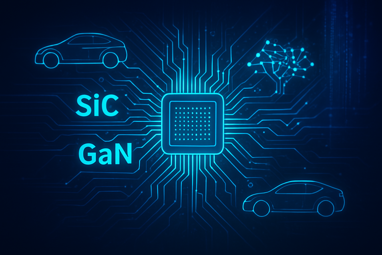
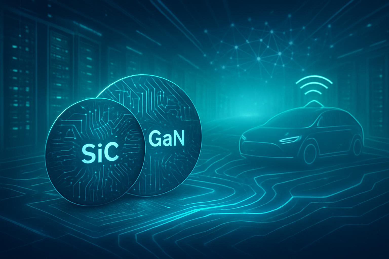
Looking further out towards 2030 and beyond, the global semiconductor market is projected to exceed $1 trillion and potentially reach $2 trillion by 2040, fueled by sustained demand for advanced technologies. Long-term developments will explore new materials beyond traditional silicon, such as germanium, graphene, gallium nitride (GaN), and silicon carbide (SiC), to push the boundaries of speed and energy efficiency. Emerging computing paradigms like neuromorphic computing, which aims to mimic the human brain's structure, and quantum computing are poised to deliver massive leaps in computational power, potentially revolutionizing fields from cryptography to material science. AI and machine learning will become even more integral to the entire chip lifecycle, from design and testing to manufacturing, optimizing processes, improving accuracy, and accelerating innovation.
These advancements will unlock a myriad of new applications and use cases. Specialized AI chips will dramatically enhance processing speeds and energy efficiency for sophisticated AI applications, including natural language processing and large language models (LLMs). Autonomous vehicles will rely heavily on advanced semiconductors for their sensor systems and real-time processing, enabling safer and more efficient transportation. The proliferation of IoT devices and Edge AI will demand power-efficient, faster chips capable of handling complex AI workloads closer to the data source. In healthcare, miniaturized sensors and processors will lead to more accurate and personalized devices, such as wearable health monitors and implantable medical solutions. Semiconductors will also play a pivotal role in energy efficiency and storage, contributing to improved solar panels, energy-efficient electronics, and advanced batteries, with wide-bandgap materials like SiC and GaN becoming core to power architectures for EVs, fast charging, and renewables.
However, this ambitious future is not without its formidable challenges. Supply chain resilience remains a persistent concern, with global events, material shortages, and geopolitical tensions continuing to disrupt the industry. The escalating geopolitical tensions and trade conflicts, particularly between major economic powers, create significant volatility and uncertainty, driving a global shift towards "semiconductor sovereignty" and increased domestic sourcing. The pervasive global shortage of skilled engineers and technicians, projected to exceed one million by 2030, represents a critical bottleneck for innovation and growth. Furthermore, the rising manufacturing costs, with leading-edge fabrication plants now exceeding $30 billion, and the increasing complexity of chip design and manufacturing continue to drive up expenses. Finally, the sustainability and environmental impact of energy-intensive manufacturing processes and the vast energy consumption of AI data centers demand urgent attention, pushing the industry towards more sustainable practices and energy-efficient designs.
Experts universally predict that the industry is firmly entrenched in an "AI Supercycle," fundamentally reorienting investment priorities and driving massive capital expenditures into advanced AI accelerators, high-bandwidth memory, and state-of-the-art fabrication facilities. Record capital expenditures, estimated at approximately $185 billion in 2025, are expected to expand global manufacturing capacity by 7%. The trend towards custom integrated circuits (ICs) will continue as companies prioritize tailored solutions for specialized performance, energy efficiency, and enhanced security. Governmental strategic investments, such as the US CHIPS Act, China's pledges, and South Korea's K-Semiconductor Strategy, underscore a global race for technological leadership and supply chain resilience. Key innovations on the horizon include on-chip optical communication using silicon photonics, continued memory innovation (HBM, GDDR7), backside or alternative power delivery, and advanced liquid cooling systems for GPU server clusters, all pointing to a future where semiconductors will remain the foundational bedrock of global technological progress.
The Silicon Horizon: A Comprehensive Wrap-up and Future Watch
The semiconductor industry is currently experiencing a profound and multifaceted transformation, largely orchestrated by the escalating demands of artificial intelligence. This era is characterized by unprecedented investment, a fundamental reshaping of market dynamics, and the laying of a crucial foundation for long-term technological and economic impacts.
Key Takeaways: The overarching theme is AI's role as the primary growth engine, driving demand for high-performance computing, data centers, High-Bandwidth Memory (HBM), and custom silicon. This marks a significant shift from historical growth drivers like smartphones and PCs to the "engines powering today's most ambitious digital revolutions." While the overall industry shows impressive growth, this benefit is highly concentrated, with the top 5% of companies generating the vast majority of economic profit. Increased capital expenditure, strategic partnerships, and robust governmental support through initiatives like the U.S. CHIPS Act are further shaping this landscape, aiming to bolster domestic supply chains and reinforce technological leadership.
Significance in AI History: The current investment trends in semiconductors are foundational to AI history. Advanced semiconductors are not merely components; they are the "lifeblood of a global AI economy," providing the immense computational power required for training and running sophisticated AI models. Data centers, powered by these advanced chips, are the "beating heart of the tech industry," with compute semiconductor growth projected to continue at an unprecedented scale. Critically, AI is not just consuming chips but also revolutionizing the semiconductor value chain itself, from design to manufacturing, marking a new, self-reinforcing investment cycle.
Long-Term Impact: The long-term impact is expected to be transformative and far-reaching. The semiconductor market is on a trajectory to reach record valuations, with AI, data centers, automotive, and IoT serving as key growth drivers through 2030 and beyond. AI will become deeply integrated into nearly every aspect of technology, sustaining revenue growth for the semiconductor sector. This relentless demand will continue to drive innovation in chip architecture, materials (like GaN and SiC), advanced packaging, and manufacturing processes. Geopolitical tensions will likely continue to influence production strategies, emphasizing diversified supply chains and regional manufacturing capabilities. The growing energy consumption of AI servers will also drive continuous demand for power semiconductors, focusing on efficiency and new power solutions.
What to Watch For: In the coming weeks and months, several critical indicators will shape the semiconductor landscape. Watch for continued strong demand in earnings reports from key AI chip manufacturers like NVIDIA (NASDAQ: NVDA), Broadcom (NASDAQ: AVGO), and TSMC (NYSE: TSM) for GPUs, HBM, and custom AI silicon. Monitor signs of recovery in legacy sectors such as automotive, analog, and IoT, which faced headwinds in 2024 but are poised for a rebound in 2025. Capital expenditure announcements from major semiconductor companies and foundries will reflect confidence in future demand and ongoing capacity expansion. Keep an eye on advancements in advanced packaging technologies, new materials, and the further integration of AI into chip design and manufacturing. Geopolitical developments and the impact of governmental support programs, alongside the market reception of new AI-powered PCs and the expansion of AI into edge devices, will also be crucial.
Connecting to ON Semiconductor's Performance: ON Semiconductor (NASDAQ: ON) provides a microcosm of the broader industry's "tale of two markets." While its Q3 2025 earnings per share exceeded analyst estimates, revenue slightly missed projections, reflecting ongoing market challenges in some segments despite signs of stabilization. The company's stock performance has seen a decline year-to-date due to cyclical slowdowns in its core automotive and industrial markets. However, ON Semiconductor is strategically positioning itself for long-term growth. Its acquisition of Vcore Power Technology in October 2025 enables it to cover the entire power chain for data center operations, a crucial area given the increasing energy demands of AI servers. This focus on power efficiency, coupled with its strengths in SiC technology and its "Fab Right" restructuring strategy, positions ON Semiconductor as a compelling turnaround story. As the automotive semiconductor market anticipates a positive long-term outlook from 2025 onwards, ON Semiconductor's strategic pivot towards AI-driven power efficiency solutions and its strong presence in automotive solutions (ADAS, EVs) suggest significant long-term growth potential, even as it navigates current market complexities.
This content is intended for informational purposes only and represents analysis of current AI developments.
TokenRing AI delivers enterprise-grade solutions for multi-agent AI workflow orchestration, AI-powered development tools, and seamless remote collaboration platforms.
For more information, visit https://www.tokenring.ai/.