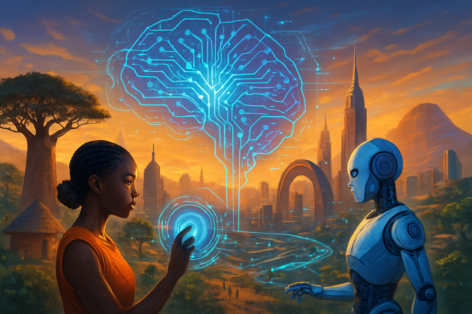
The biopharmaceutical industry is undergoing an immediate and profound transformation, as Artificial Intelligence (AI) rapidly compresses timelines, drastically reduces costs, and significantly enhances the precision of drug development from initial discovery to commercial manufacturing. This fundamental shift is giving rise to the "TechBio" era, where AI is no longer merely a supporting tool but the central engine driving innovation and defining competitive advantage.
Currently, AI's impact is revolutionizing every facet of the biopharmaceutical value chain. In drug discovery, advanced AI models are accelerating target identification, enabling de novo drug design to create novel molecules from scratch, and performing virtual screenings of millions of compounds in a fraction of the time, dramatically reducing the need for extensive physical testing and cutting discovery costs by up to 40%. This accelerated approach extends to preclinical development, where AI-powered computational simulations, or "digital twins," predict drug safety and efficacy more rapidly than traditional animal testing. Beyond discovery, AI is optimizing clinical trial design, streamlining patient recruitment, and enhancing monitoring, with predictions suggesting a doubling of AI adoption in clinical development in 2025 alone. In manufacturing, AI and automation are boosting production efficiency, improving quality control, enabling real-time issue identification, and optimizing complex supply chains through predictive analytics and continuous manufacturing systems, ultimately reducing human error and waste. The emergence of the 'TechBio' era signifies this radical change, marking a period where "AI-first" biotech firms are leading the charge, integrating AI as the backbone of their operations to decode complex biological systems and deliver life-saving therapies with unprecedented speed and accuracy.
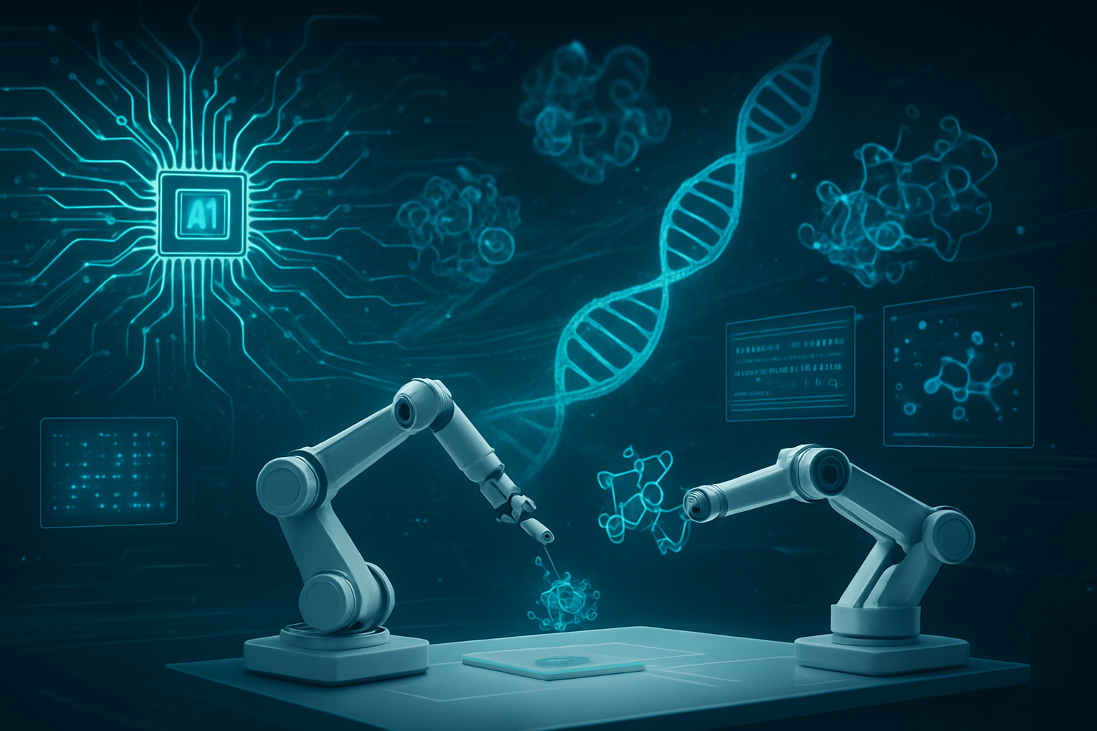
AI's Technical Prowess Reshaping Drug Discovery and Development
Artificial intelligence (AI) is rapidly transforming the biopharmaceutical landscape, fundamentally reshaping processes across drug discovery, development, and manufacturing. In drug discovery, generative AI stands out as a pivotal advancement, capable of designing novel molecular structures and chemical compounds from scratch (de novo drug design) by learning from vast datasets of known chemical entities. This capability significantly accelerates lead generation and optimization, allowing for the rapid exploration of a chemical space estimated to contain over 10^60 possible drug-like molecules, a feat impossible with traditional, labor-intensive screening methods. Technical specifications include deep learning algorithms, such as Generative Adversarial Networks (GANs), which predict compound properties like solubility, bioavailability, efficacy, and toxicity with unprecedented accuracy, thereby reducing the number of compounds that need physical synthesis and testing. This contrasts sharply with conventional approaches that often rely on the slower, more costly identification and modification of existing compounds and extensive experimental testing. The AI research community and industry experts view this as transformative, promising quicker cures at a fraction of the cost by enabling a more nuanced and precise optimization of drug candidates.
In drug development, particularly within clinical trials, AI and machine learning (ML) are optimizing design and execution, addressing long-standing inefficiencies and high failure rates. ML algorithms analyze large, diverse datasets—including electronic health records, genomics, and past trial performance—to precisely identify eligible patient populations, forecast enrollment bottlenecks, and detect variables influencing patient adherence. Predictive analytics allows for the optimization of trial protocols, real-time data monitoring for early safety signals, and the adjustment of trial parameters adaptively, leading to more robust study designs. For instance, AI can significantly reduce patient screening time by 34% and increase trial enrollment by 11% by automating the review of patient criteria and eligibility. This is a substantial departure from traditional, often exhaustive and inefficient trial designs that rely heavily on manual processes and historical data, which can lead to high failure rates and significant financial losses. Early results for AI-discovered drugs show promising success rates in Phase I clinical trials (80-90% compared to traditional 40-65%), though Phase II rates are comparable to historical averages, indicating continued progress is needed.
Furthermore, AI is revolutionizing biopharmaceutical manufacturing by enhancing efficiency, quality, and consistency. Machine learning and predictive analytics are key technologies, leveraging algorithms to analyze historical process data from sensors, equipment, and quality control tests. These models forecast outcomes, identify anomalies, and optimize production parameters in real time, such as temperature, pH, and nutrient levels in fermentation and cell culture. This capability allows for predictive maintenance, anticipating equipment failures before they occur, thereby minimizing downtime and production disruptions. Unlike traditional manufacturing, which often involves labor-intensive batch processing susceptible to variability, AI-driven systems support continuous manufacturing with real-time adjustments, ensuring higher productivity and consistent product quality. The integration of AI also extends to supply chain management, optimizing inventory and logistics through demand forecasting. Industry experts highlight AI's ability to shift biomanufacturing from a reactive to a predictive paradigm, leading to increased yields, reduced costs, and improved product quality, ultimately ensuring higher quality biologics reach patients more reliably.
The initial reactions from both the AI research community and biopharma industry experts are largely optimistic, hailing AI as a "game-changer" and a "new catalyst" that accelerates innovation and enhances precision across the entire value chain. While recognizing AI's transformative potential to compress timelines and reduce costs significantly—potentially cutting drug development from 13 years to around 8 years and costs by up to 75%—experts also emphasize that AI is an "enhancer, not a replacement for human expertise and creativity." Challenges remain, including the need for high-quality data, addressing ethical concerns like AI bias, navigating regulatory complexities, and integrating AI into existing infrastructure. There is a consensus that successful AI adoption requires a collaborative approach between AI researchers and pharmaceutical scientists, alongside a shift in mindset within organizations to prioritize governance, transparency, and continuous workforce upskilling to harness these powerful tools responsibly.
Competitive Landscape: Who Benefits in the TechBio Era?
AI advancements are profoundly reshaping the biopharma and TechBio landscapes, creating new opportunities and competitive dynamics for AI companies, tech giants, and startups. Major pharmaceutical companies such as Pfizer (NYSE: PFE), Novartis (NYSE: NVS), Roche (SIX: ROG), AstraZeneca (NASDAQ: AZN), Sanofi (NASDAQ: SNY), Merck (NYSE: MRK), Lilly (NYSE: LLY), and Novo Nordisk (NYSE: NVO) are strategically integrating AI into their operations, recognizing its potential to accelerate drug discovery, optimize clinical development, and enhance manufacturing processes. These established players stand to benefit immensely by leveraging AI to reduce R&D costs, shorten time-to-market for new therapies, and achieve significant competitive advantages in drug efficacy and operational efficiency. For instance, Lilly is deploying an "AI factory" with NVIDIA's DGX SuperPOD to compress drug discovery timelines and enable breakthroughs in genomics and personalized medicine, while Sanofi is partnering with OpenAI and Formation Bio to build pharma-specific foundation models.
Tech giants and major AI labs are becoming indispensable partners and formidable competitors in this evolving ecosystem. Companies like Google (NASDAQ: GOOGL) (through Verily and Isomorphic Labs), Microsoft (NASDAQ: MSFT), Amazon (NASDAQ: AMZN) (AWS), and Nvidia (NASDAQ: NVDA) are crucial for providing the foundational cloud computing infrastructure, AI platforms (e.g., NVIDIA BioNeMo, Microsoft Azure), and specialized machine learning services that biopharma companies require. This creates new, substantial revenue streams for tech giants and deepens their penetration into the healthcare sector, especially for pharma companies that lack extensive in-house AI capabilities. Beyond infrastructure, some tech giants are directly entering drug discovery, with Google's Isomorphic Labs utilizing AI to tackle complex biological problems. The competitive implications for these entities include solidifying their positions as essential technology providers and potentially directly challenging traditional biopharma in drug development. The disruption to existing products and services is significant, as AI-driven approaches are replacing traditionally manual, time-consuming, and expensive processes, leading to a leaner, faster, and more data-driven operating model across the entire drug value chain.
Meanwhile, specialized AI companies and TechBio startups are at the forefront of innovation, driving much of the disruption. Companies like Insilico Medicine, Atomwise, Exscientia, BenevolentAI, Recursion, Iktos, Cradle Bio, and Antiverse are leveraging AI and deep learning for accelerated target identification, novel molecule generation, and predictive analytics in drug discovery. These agile startups are attracting significant venture capital and forming strategic collaborations with major pharmaceutical firms, often bringing drug candidates into clinical stages at unprecedented speeds and reduced costs. Their strategic advantage lies in their AI-first platforms and ability to swiftly analyze vast datasets, optimize clinical trial design, and even develop personalized medicine. Market positioning emphasizes cutting-edge technology and efficiency, with some startups focusing on specific niches like antibody design or gene therapies. The potential disruption to existing products and services is immense, as AI-driven processes promise to reduce drug discovery timelines from years to months and slash R&D costs by up to 40%, ultimately leading to more personalized, accessible, and effective healthcare solutions.
Wider Significance: AI's Broad Impact and Ethical Imperatives
Artificial intelligence (AI) is ushering in a transformative era for biopharma, particularly within the burgeoning "TechBio" landscape, which represents the convergence of life sciences and advanced technology. AI's wider significance lies in its profound ability to accelerate and enhance nearly every stage of drug discovery, development, and delivery, moving away from traditional, lengthy, and costly methods. By leveraging machine learning, deep learning, and generative AI, biopharma companies can sift through massive datasets—including genomic profiles, electronic health records, and chemical libraries—at unprecedented speeds, identifying potential drug candidates, predicting molecular interactions, and designing novel compounds with greater precision. This data-driven approach is fundamentally reshaping target identification, virtual screening, and the optimization of clinical trials, leading to a significant reduction in development timelines and costs. For instance, early discovery could see time and cost savings of 70-80%, and AI-discovered molecules are showing remarkable promise with 80-90% success rates in Phase I clinical trials, a substantial improvement over traditional rates of 40-65%. Beyond drug development, AI is crucial for personalized medicine, enabling the tailoring of treatments based on individual patient characteristics, and for revolutionizing diagnostics and medical imaging, facilitating earlier disease detection and more accurate interpretations. Generative AI, in particular, is not just a buzzword but is driving meaningful transformation, actively being used by a high percentage of pharma and biotech firms, and is projected to unlock billions in value for the life sciences sector.
This profound integration of AI into biopharma aligns perfectly with broader AI landscape trends, particularly the advancements in deep learning, large language models, and the increasing computational power available for processing "big data." The biopharma sector is adopting cutting-edge AI techniques such as natural language processing and computer vision to analyze complex biological and chemical information, a testament to the versatility of modern AI algorithms. The emergence of tools like AlphaFold, which utilizes deep neural networks to predict 3D protein structures, exemplifies how AI is unlocking a deeper understanding of biological systems previously unimaginable, akin to providing a "language to learn the rules of biology". Furthermore, the industry is looking towards "agentic AI" and "physical AI," including robotics, to further automate routine tasks, streamline decision-making, and even assist in complex procedures like surgery, signifying a continuous evolution of AI's role from analytical support to autonomous action. This reflects a general trend across industries where AI is moving from niche applications to foundational, pervasive technologies that redefine operational models and foster unprecedented levels of innovation.
However, the expansive role of AI in biopharma also brings broader impacts and potential concerns that need careful consideration. The positive impacts are immense: faster development of life-saving therapies, more effective and personalized treatments for complex and rare diseases, improved patient outcomes through precision diagnostics, and significant cost reductions across the value chain. Yet, these advancements are accompanied by critical ethical and practical challenges. Chief among them are concerns regarding data privacy and security, as AI systems rely on vast amounts of highly sensitive patient data, including genetic information, raising risks of breaches and misuse. Algorithmic bias is another major concern; if AI models are trained on unrepresentative datasets, they can perpetuate existing health disparities by recommending less effective or even harmful treatments for underrepresented populations. The "black box" nature of some advanced AI models also poses challenges for transparency and explainability, making it difficult for regulators, clinicians, and patients to understand how critical decisions are reached. Furthermore, defining accountability for AI-driven errors in R&D or clinical care remains a complex ethical and legal hurdle, necessitating robust regulatory alignment and ethical frameworks to ensure responsible innovation.
Compared to previous AI milestones, the current impact of AI in biopharma signifies a qualitative leap. Earlier AI breakthroughs, such as those in chess or image recognition, often tackled problems within well-defined, somewhat static environments. In contrast, AI in biopharma grapples with the inherent complexity and unpredictability of biological systems, a far more challenging domain. While computational chemistry and bioinformatics have been used for decades, modern AI, particularly deep learning and generative models, moves beyond mere automation to truly generate new hypotheses, drug structures, and insights that were previously beyond human capacity. For example, the capability of generative AI to "propose something that was previously unknown" in drug design marks a significant departure from earlier, more constrained computational methods. This shift is not just about speed and efficiency, but about fundamentally transforming the scientific discovery process itself, enabling de novo drug design and a level of personalized medicine that was once aspirational. The current era represents a maturation of AI, where its analytical power is now robust enough to meaningfully interrogate and innovate within the intricate and dynamic world of living systems.
The Horizon: Future Developments and Enduring Challenges
Artificial intelligence (AI) is rapidly transforming the biopharmaceutical and TechBio landscape, shifting from an emerging trend to a foundational engine driving innovation across the sector. In the near term, AI is significantly accelerating drug discovery by optimizing molecular design, identifying high-potential drug candidates with greater precision, and reducing costs and timelines. It plays a crucial role in optimizing clinical trials through smarter patient selection, efficient recruitment, and real-time monitoring of patient data to detect adverse reactions early, thereby reducing time-to-market. Beyond research and development, AI is enhancing biopharma manufacturing by optimizing process design, improving real-time quality control, and boosting overall operational efficiency, leading to higher precision and reduced waste. Furthermore, AI is proving valuable in drug repurposing, identifying new therapeutic uses for existing drugs by analyzing vast datasets and uncovering hidden relationships between drugs and diseases.
Looking further ahead, the long-term developments of AI in biopharma promise even more profound transformations. Experts predict that AI will enable more accurate biological models, leading to fewer drug failures in clinical trials. The industry will likely see a significant shift towards personalized medicine and therapies, with AI facilitating the development of custom-made treatment plans based on individual genetic profiles and responses to medication. Advanced AI integration will lead to next-generation smart therapeutics and real-time patient monitoring, marrying technology with biology in unprecedented ways. The convergence of AI with robotics and automation is expected to drive autonomous labs, allowing for experimentation cycles to be executed with greater consistency, fewer errors, and significantly shorter timeframes. By 2030, a substantial portion of drug discovery is expected to be conducted in silico and in collaboration with academia, drastically reducing the time from screening to preclinical testing to a few months.
Despite these promising advancements, several challenges need to be addressed for AI to fully realize its potential in biopharma. Key hurdles include ensuring data privacy, security, quality, and availability, as AI models require large volumes of high-quality data for training. Regulatory compliance and the ethical considerations surrounding AI algorithms for decision-making in clinical trials also present significant challenges. Integrating AI with existing legacy systems and managing organizational change, along with a shortage of skilled AI talent, are further obstacles. Experts predict that AI will become a cornerstone of the pharmaceutical and biotech sector in the next decade, enhancing success rates in drug discovery, optimizing production lines, and improving supply chain efficiency. The successful integration of AI requires not only technological investment but also a commitment to responsible innovation, ensuring ethical data practices and transparent decision-making processes to deliver both operational excellence and ethical integrity across the value chain. Companies that act decisively in addressing these challenges and prioritize AI investments are expected to gain a competitive edge in cost efficiency, quality, innovation, and sustainability.
A New Dawn: The Enduring Impact of AI in Biopharma
The integration of Artificial Intelligence (AI) into biopharma and the burgeoning TechBio era marks a pivotal shift in the landscape of drug discovery and development. Key takeaways highlight AI's profound ability to accelerate processes, reduce costs, and enhance success rates across the entire drug development pipeline. AI is being leveraged from initial target identification and lead optimization to patient stratification for clinical trials and even drug repurposing. Generative AI, in particular, is revolutionizing molecular design and understanding protein structures, with breakthroughs like AlphaFold demonstrating AI's capacity to solve long-standing biological challenges. This technological advancement is not merely incremental; it represents a significant milestone in AI history, moving from theoretical capabilities to tangible, life-saving applications in a highly complex and regulated industry. The emergence of "AI-first" biotech companies and strategic alliances between pharmaceutical giants and AI innovators underscore this transformative period, signaling a future where AI is an indispensable tool for scientific progress.
Looking ahead, the long-term impact of AI in biopharma is poised to deliver a deeper understanding of disease biology, enable more effective and personalized treatments, and ultimately lead to faster cures and improved patient outcomes globally. While the benefits are immense, challenges remain, including ensuring high-quality data, addressing potential algorithmic biases, developing robust regulatory frameworks, and seamlessly integrating AI into existing workflows. Despite these hurdles, the momentum is undeniable, with AI-driven drug candidates exponentially increasing in clinical trials. In the coming weeks and months, critical areas to watch include the continued evolution of generative AI capabilities, particularly in multi-omics data integration and the design of novel therapeutics like mRNA vaccines and PROTACs. We should also anticipate further clarity in regulatory guidelines for AI-driven therapies, sustained investment and partnerships between tech and biopharma, and, most crucially, the performance and success rates of AI-discovered drugs as they progress through later stages of clinical development. The industry is currently in an exciting phase, where the promise of AI is increasingly being validated by concrete results, laying the groundwork for a truly revolutionized biopharmaceutical future.
This content is intended for informational purposes only and represents analysis of current AI developments.
TokenRing AI delivers enterprise-grade solutions for multi-agent AI workflow orchestration, AI-powered development tools, and seamless remote collaboration platforms.
For more information, visit https://www.tokenring.ai/.