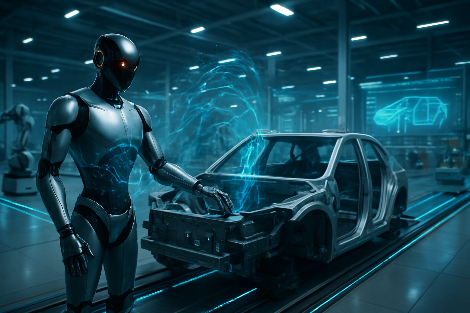
In a landmark moment for the commercialization of humanoid robotics, Boston Dynamics has officially moved its all-electric Atlas robot from the laboratory to the factory floor. As of January 2026, the company—wholly owned by the Hyundai Motor Company (KRX: 005380)—has begun the industrial deployment of its next-generation humanoid at the Hyundai Motor Group Metaplant America (HMGMA) in Savannah, Georgia. This shift marks the transition of Atlas from a viral research sensation to a functional industrial asset, specialized for heavy lifting and autonomous parts sequencing within one of the world's most advanced automotive manufacturing hubs.
The deployment centers on the "Software-Defined Factory" (SDF) philosophy, where hardware and software are seamlessly integrated to allow for rapid iteration and real-time optimization. At the HMGMA, Atlas is no longer performing the backflips that made its hydraulic predecessor famous; instead, it is tackling the "dull, dirty, and dangerous" tasks of a live production environment. By automating the movement of heavy components and organizing parts for human assembly lines, Hyundai aims to set a new global standard for the "Metaplant" of the future, leveraging what experts are calling "Physical AI."
Precision Power: The Technical Architecture of the Electric Atlas
The all-electric Atlas represents a radical departure from the hydraulic architecture that defined the platform for over a decade. While the previous model was a marvel of power density, its reliance on high-pressure pumps and hoses made it noisy, prone to leaks, and difficult to maintain in a sterile factory environment. The new 2026 production model utilizes custom-designed electric direct-drive actuators with a staggering torque density of 220 Nm/kg. This allows the robot to maintain a sustained payload capacity of 66 lbs (30 kg) and a burst-lift capability of up to 110 lbs (50 kg), comfortably handling the heavy engine components and battery modules typical of electric vehicle (EV) production.
Technical specifications for the electric Atlas include 56 degrees of freedom—nearly triple that of the hydraulic version—and many of its joints are capable of full 360-degree rotation. This "superhuman" range of motion allows the robot to navigate cramped warehouse aisles by spinning its torso or limbs rather than turning its entire base, minimizing its footprint and increasing efficiency. Its perception system has been upgraded to a 360-degree sensor suite utilizing LiDAR and high-resolution cameras, processed locally by an onboard NVIDIA Corporation (NASDAQ: NVDA) Jetson Thor platform. This provides the robot with total spatial awareness, allowing it to operate safely alongside human workers without the need for safety cages.
Initial reactions from the robotics community have been overwhelmingly positive, with researchers noting that the move to electric actuators simplifies the control stack significantly. Unlike previous approaches that required complex fluid dynamics modeling, the electric Atlas uses high-fidelity force control and tactile-sensing hands. This allows it to perform "blind" manipulations—sensing the weight and friction of an object through its fingertips—much like a human worker, which is critical for tasks like threading bolts or securing delicate wiring harnesses.
The Humanoid Arms Race: Competitive and Strategic Implications
The deployment at the Georgia Metaplant places Hyundai at the forefront of a burgeoning "Humanoid Arms Race," directly challenging the progress of Tesla (NASDAQ: TSLA) and its Optimus program. While Tesla has emphasized high-volume production and vertical integration, Hyundai’s strategy leverages the decades of R&D expertise from Boston Dynamics combined with one of the largest manufacturing footprints in the world. By treating the Georgia facility as a "live laboratory," Hyundai is effectively bypassing the simulation-to-reality gap that has slowed other competitors.
This development is also a major win for the broader AI ecosystem. The electric Atlas’s "brain" is the result of collaboration between Boston Dynamics and Alphabet Inc. (NASDAQ: GOOGL) via its DeepMind unit, focusing on Large Behavior Models (LBM). These models enable the robot to handle "unstructured" environments—meaning it can figure out what to do if a parts bin is slightly out of place or if a component is dropped. This level of autonomy disrupts the traditional industrial robotics market, which has historically relied on fixed-path programming. Startups focusing on specialized robotic components, such as high-torque motors and haptic sensors, are likely to see increased investment as the demand for humanoid-scale parts scales toward mass production.
Strategically, the HMGMA deployment serves as a blueprint for the "Robot Metaplant Application Center" (RMAC). This facility acts as a validation hub where manufacturing data is fed into Atlas’s AI models to ensure 99.9% reliability. By proving the technology in their own plants first, Hyundai and Boston Dynamics are positioning themselves to sell not just robots, but entire autonomous labor solutions to other industries, from aerospace to logistics.
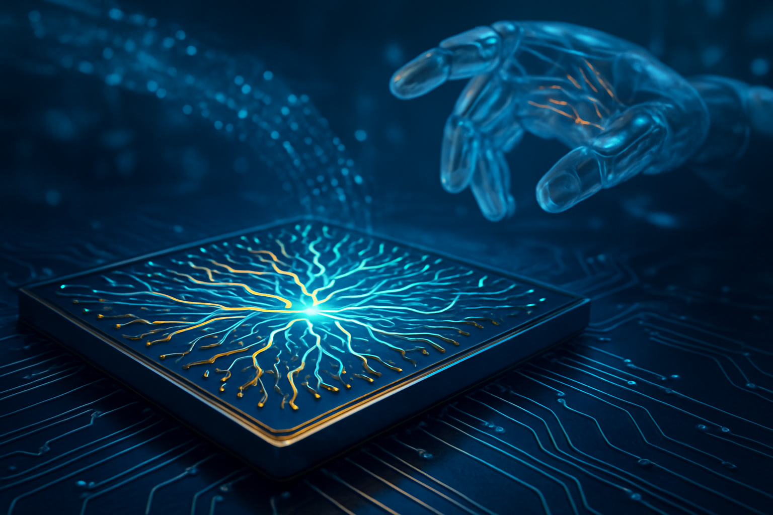
Physical AI and the Broader Landscape of Automation
The integration of Atlas into the Georgia Metaplant is a milestone in the rise of "Physical AI"—the application of advanced machine learning to the physical world. For years, AI breakthroughs were largely confined to the digital realm, such as Large Language Models and image generation. However, the deployment of Atlas signifies that AI has matured enough to manage the complexities of gravity, friction, and multi-object interaction in real time. This move mirrors the "GPT-3 moment" for robotics, where the technology moves from an impressive curiosity to an essential tool for global industry.
However, the shift is not without its concerns. The prospect of 30,000 humanoid units per year, as projected by Hyundai for the end of the decade, raises significant questions regarding the future of the manufacturing workforce. While Hyundai maintains that Atlas is designed to augment human labor by taking over the most strenuous tasks, labor economists warn of potential displacement in traditional assembly roles. The broader significance lies in how society will adapt to a world where "general-purpose" robots can be retrained for new tasks overnight simply by downloading a new software update, much like a smartphone app.
Compared to previous milestones, such as the first deployment of UNIMATE in the 1960s, the Atlas rollout is uniquely collaborative. The use of "Digital Twins" allows engineers in South Korea to simulate tasks in a virtual environment before "pushing" the code to robots in Georgia. This global, cloud-based approach to labor is a fundamental shift in how manufacturing is conceptualized, turning a physical factory into a programmable asset.
The Road Ahead: From Parts Sequencing to Full Assembly
In the near term, we can expect the fleet of Atlas robots at the HMGMA to expand from a handful of pilot units to a full-scale workforce. The immediate focus remains on parts sequencing and material handling, but the roadmap for 2027 and 2028 includes more complex assembly tasks. These will include the installation of interior trim and the routing of EV cooling systems—tasks that require the high dexterity and fine motor skills that Boston Dynamics is currently refining in the RMAC.
Looking further ahead, the goal is for Atlas to reach a state of "unsupervised autonomy," where it can self-diagnose mechanical issues and navigate to autonomous battery-swapping stations without human intervention. The challenges remaining are significant, particularly in the realm of long-term durability and the energy density of batteries required for a full 8-hour shift of heavy lifting. However, experts predict that as the "Software-Defined Factory" matures, the hardware will become increasingly modular, allowing for "hot-swapping" of limbs or sensors in minutes rather than hours.
A New Chapter in Robotics History
The deployment of the all-electric Atlas at Hyundai’s Georgia Metaplant is more than just a corporate milestone; it is a signal that the era of the general-purpose humanoid has arrived. By moving beyond the hydraulic prototypes of the past and embracing a software-first, all-electric architecture, Boston Dynamics and Hyundai have successfully bridged the gap between a high-tech demo and an industrial workhorse.
The coming months will be critical as the HMGMA scales its production of EVs and its integration of robotic labor. Observers should watch for the reliability metrics coming out of the Savannah facility and the potential for Boston Dynamics to announce third-party pilot programs with other industrial giants. While the backflips may be over, the real work for Atlas—and the future of the global manufacturing sector—has only just begun.
This content is intended for informational purposes only and represents analysis of current AI developments.
TokenRing AI delivers enterprise-grade solutions for multi-agent AI workflow orchestration, AI-powered development tools, and seamless remote collaboration platforms.
For more information, visit https://www.tokenring.ai/.