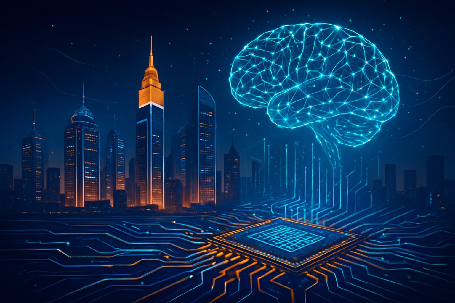
Significant investments in Artificial Intelligence (AI) are igniting an unprecedented boom in the semiconductor industry, propelling demand for advanced chip technology and specialized manufacturing equipment to new heights. As of late 2025, this symbiotic relationship between AI and semiconductors is not merely a trend but a full-blown "AI Supercycle," fundamentally reshaping global technology markets and driving innovation at an accelerated pace. The insatiable appetite for computational power, particularly from large language models (LLMs) and generative AI, has shifted the semiconductor industry's primary growth engine from traditional consumer electronics to high-performance AI infrastructure.
This surge in capital expenditure, with big tech firms alone projected to invest hundreds of billions in AI infrastructure in 2025, is translating directly into soaring orders for advanced GPUs, high-bandwidth memory (HBM), and cutting-edge manufacturing equipment. The immediate significance lies in a profound transformation of the global supply chain, a race for technological supremacy, and a rapid acceleration of innovation across the entire tech ecosystem. This period is marked by an intense focus on specialized hardware designed to meet AI's unique demands, signaling a new era where hardware breakthroughs are as critical as algorithmic advancements for the future of artificial intelligence.
The Technical Core: Unpacking AI's Demands and Chip Innovations
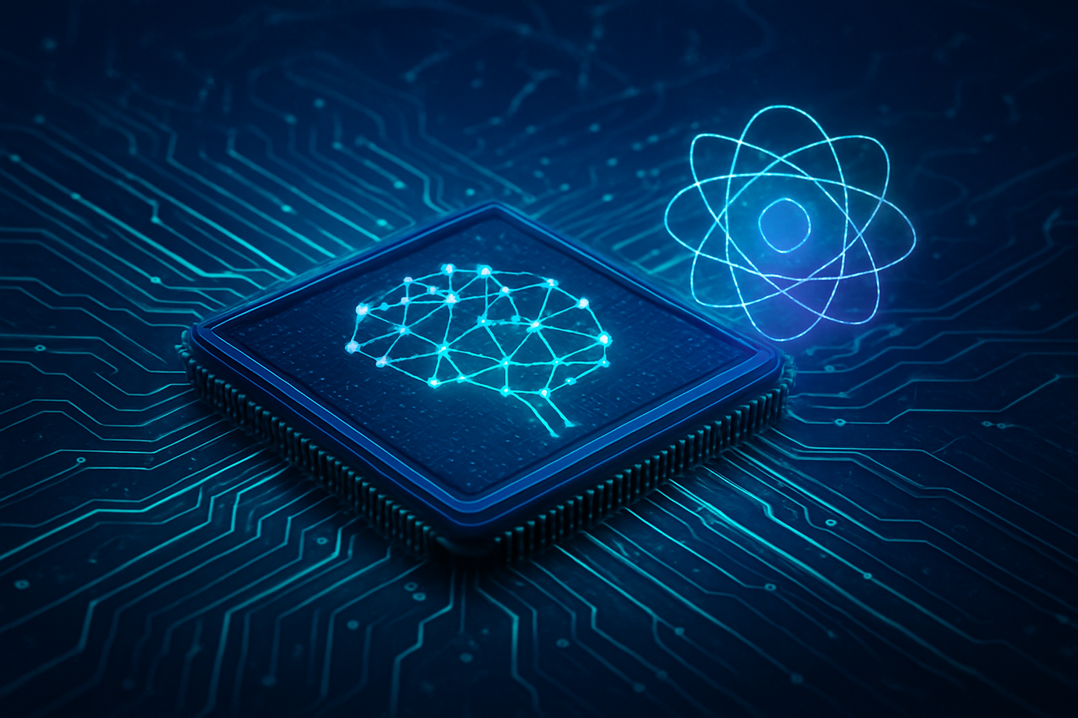
The driving force behind this semiconductor surge lies in the specific, demanding technical requirements of modern AI, particularly Large Language Models (LLMs) and Generative AI. These models, built upon the transformer architecture, process immense datasets and perform billions, if not trillions, of calculations to understand, generate, and process complex content. This computational intensity necessitates specialized hardware that significantly departs from previous general-purpose computing approaches.
At the forefront of this hardware revolution are GPUs (Graphics Processing Units), which excel at the massive parallel processing and matrix multiplication operations fundamental to deep learning. Companies like Nvidia (NASDAQ: NVDA) have seen their market capitalization soar, largely due to the indispensable role of their GPUs in AI training and inference. Beyond GPUs, ASICs (Application-Specific Integrated Circuits), exemplified by Google's Tensor Processing Units (TPUs), offer custom-designed efficiency, providing superior speed, lower latency, and reduced energy consumption for particular AI workloads.
Crucial to these AI accelerators is HBM (High-Bandwidth Memory). HBM overcomes the traditional "memory wall" bottleneck by vertically stacking memory chips and connecting them with ultra-wide data paths, placing memory closer to the processor. This 3D stacking dramatically increases data transfer rates and reduces power consumption, making HBM3e and the emerging HBM4 indispensable for data-hungry AI applications. SK Hynix (KRX: 000660) and Samsung Electronics (KRX: 005930) are key suppliers, reportedly selling out their HBM capacity for 2025.
Furthermore, advanced packaging technologies like TSMC's (TPE: 2330) CoWoS (Chip on Wafer on Substrate) are critical for integrating multiple chips—such as GPUs and HBM—into a single, high-performance unit. CoWoS enables 2.5D and 3D integration, creating short, high-bandwidth connections that significantly reduce signal delay. This heterogeneous integration allows for greater transistor density and computational power in a smaller footprint, pushing performance beyond traditional planar scaling limits. The relentless pursuit of advanced process nodes (e.g., 3nm and 2nm) by leading foundries like TSMC and Samsung further enhances chip performance and energy efficiency, leveraging innovations like Gate-All-Around (GAA) transistors.
The AI research community and industry experts have reacted with a mix of awe and urgency. There's widespread acknowledgment that generative AI and LLMs represent a "major leap" in human-technology interaction, but are "extremely computationally intensive," placing "enormous strain on training resources." Experts emphasize that general-purpose processors can no longer keep pace, necessitating a profound transformation towards hardware designed from the ground up for AI tasks. This symbiotic relationship, where AI's growth drives chip demand and semiconductor breakthroughs enable more sophisticated AI, is seen as a "new S-curve" for the industry. However, concerns about data quality, accuracy issues in LLMs, and integration challenges are also prominent.
Corporate Beneficiaries and Competitive Realignment
The AI-driven semiconductor boom is creating a seismic shift in the corporate landscape, delineating clear beneficiaries, intensifying competition, and necessitating strategic realignments across AI companies, tech giants, and startups.
Nvidia (NASDAQ: NVDA) stands as the most prominent beneficiary, solidifying its position as the world's first $5 trillion company. Its GPUs remain the gold standard for AI training and inference, making it a pivotal player often described as the "Federal Reserve of AI." However, competitors are rapidly advancing: Advanced Micro Devices (NASDAQ: AMD) is aggressively expanding its Instinct MI300 and MI350 series GPUs, securing multi-billion dollar deals to challenge Nvidia's market share. Intel (NASDAQ: INTC) is also making significant strides with its foundry business and AI accelerators like Gaudi 3, aiming to reclaim market leadership.
The demand for High-Bandwidth Memory (HBM) has translated into surging profits for memory giants SK Hynix (KRX: 000660) and Samsung Electronics (KRX: 005930), both experiencing record sales and aggressive capacity expansion. As the leading pure-play foundry, Taiwan Semiconductor Manufacturing Company (TSMC) (TPE: 2330) is indispensable, reporting significant revenue growth from its cutting-edge 3nm and 5nm chips, essential for AI accelerators. Other key beneficiaries include Broadcom (NASDAQ: AVGO), a major AI chip supplier and networking leader, and Qualcomm (NASDAQ: QCOM), which is challenging in the AI inference market with new processors.
Tech giants like Microsoft (NASDAQ: MSFT), Amazon (NASDAQ: AMZN), and Alphabet (NASDAQ: GOOGL) are heavily investing in AI infrastructure, leveraging their cloud platforms to offer AI-as-a-service. Many are also developing custom in-house AI chips to reduce reliance on external suppliers and optimize for their specific workloads. This vertical integration is a key competitive strategy, allowing for greater control over performance and cost. Startups, while benefiting from increased investment, face intense competition from these giants, leading to a consolidating market where many AI pilots fail to deliver ROI.
Crucially, companies providing the tools to build these advanced chips are also thriving. KLA Corporation (NASDAQ: KLAC), a leader in process control and defect inspection, has received significant positive market feedback. Wall Street analysts highlight that accelerating AI investments are driving demand for KLA's critical solutions in compute, memory, and advanced packaging. KLA, with a dominant 56% market share in process control, expects its advanced packaging revenue to surpass $925 million in 2025, a remarkable 70% surge from 2024, driven by AI and process control demand. Analysts like Stifel have reiterated a "Buy" rating with raised price targets, citing KLA's consistent growth and strategic positioning in an industry poised for trillion-dollar sales by 2030.
Wider Implications and Societal Shifts
The monumental investments in AI and the subsequent explosion in semiconductor demand are not merely technical or economic phenomena; they represent a profound societal shift with far-reaching implications, both beneficial and concerning. This trend fits into a broader AI landscape defined by rapid scaling and pervasive integration, where AI is becoming a foundational layer across all technology.
This "AI Supercycle" is fundamentally different from previous tech booms. Unlike past decades where consumer markets drove chip demand, the current era is dominated by the insatiable appetite for AI data center chips. This signifies a deeper, more symbiotic relationship where AI isn't just a software application but is deeply intertwined with hardware innovation. AI itself is even becoming a co-architect of its infrastructure, with AI-powered Electronic Design Automation (EDA) tools dramatically accelerating chip design, creating a virtuous "self-improving loop." This marks a significant departure from earlier technological revolutions where AI was not actively involved in the chip design process.
The overall impacts on the tech industry and society are transformative. Economically, the global semiconductor industry is projected to reach $800 billion in 2025, with forecasts pushing towards $1 trillion by 2028. This fuels aggressive R&D, leading to more efficient and innovative chips. Beyond tech, AI-driven semiconductor advancements are spurring transformations in healthcare, finance, manufacturing, and autonomous systems. However, this growth also brings critical concerns:
- Environmental Concerns: The energy consumption of AI data centers is alarming, projected to consume up to 12% of U.S. electricity by 2028 and potentially 20% of global electricity by 2030-2035. This strains power grids, raises costs, and hinders clean energy transitions. Semiconductor manufacturing is also highly water-intensive, and rapid hardware obsolescence contributes to escalating electronic waste. There's an urgent need for greener practices and sustainable AI growth.
- Ethical Concerns: While the immediate focus is on hardware, the widespread deployment of AI enabled by these chips raises substantial ethical questions. These include the potential for AI algorithms to perpetuate societal biases, significant privacy concerns due to extensive data collection, questions of accountability for AI decisions, potential job displacement, and the misuse of advanced AI for malicious purposes like surveillance or disinformation.
- Geopolitical Concerns: The concentration of advanced chip manufacturing in Asia, particularly with TSMC, is a major geopolitical flashpoint. This has led to trade wars, export controls, and a global race for technological sovereignty, with nations investing heavily in domestic production to diversify supply chains and mitigate risks. The talent shortage in the semiconductor industry is further exacerbated by geopolitical competition for skilled professionals.
Compared to previous AI milestones, this era is characterized by unprecedented scale and speed, a profound hardware-software symbiosis, and AI's active role in shaping its own physical infrastructure. It moves beyond traditional Moore's Law scaling, emphasizing advanced packaging and 3D integration to achieve performance gains.
The Horizon: Future Developments and Looming Challenges
Looking ahead, the trajectory of AI investments and semiconductor demand points to an era of continuous, rapid evolution, bringing both groundbreaking applications and formidable challenges.
In the near term (2025-2030), autonomous AI agents are expected to become commonplace, with over half of companies deploying them by 2027. Generative AI will be ubiquitous, increasingly multimodal, capable of generating text, images, audio, and video. AI agents will evolve towards self-learning, collaboration, and emotional intelligence. Chip technology will be dominated by the widespread adoption of advanced packaging, which is projected to achieve 90% penetration in PCs and graphics processors by 2033, and its market in AI chips is forecast to reach $75 billion by 2033.
For the long term (beyond 2030), AI scaling is anticipated to continue, driving the global economy to potentially $15.7 trillion by 2030. AI is expected to revolutionize scientific R&D, assisting with complex scientific software, mathematical proofs, and biological protocols. A significant long-term chip development is neuromorphic computing, which aims to mimic the human brain's energy efficiency and power. Neuromorphic chips could power 30% of edge AI devices by 2030 and reduce AI's global energy consumption by 20%. Other trends include smaller process nodes (3nm and beyond), chiplet architectures, and AI-powered chip design itself, optimizing layouts and performance.
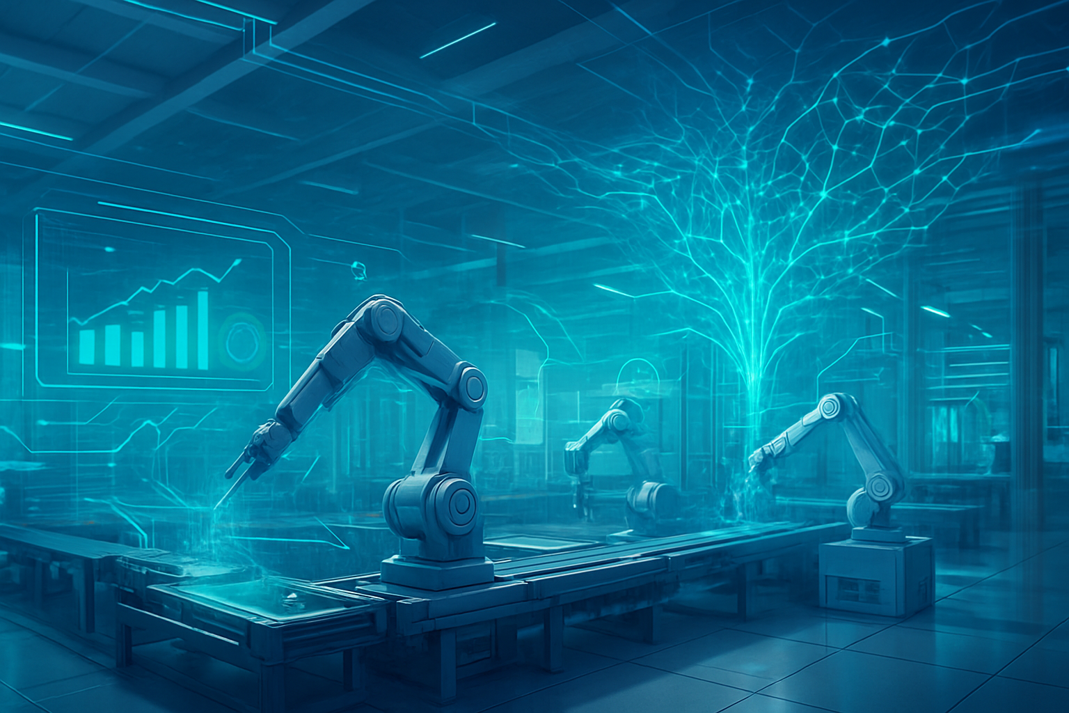
Potential applications on the horizon are vast, spanning healthcare (accelerated drug discovery, precision medicine), finance (advanced fraud detection, autonomous finance), manufacturing and robotics (predictive analytics, intelligent robots), edge AI and IoT (intelligence in smart sensors, wearables, autonomous vehicles), education (personalized learning), and scientific research (material discovery, quantum computing design).
However, realizing this future demands addressing critical challenges:
- Energy Consumption: The escalating power demands of AI data centers are unsustainable, stressing grids and increasing carbon emissions. Solutions require more energy-efficient chips, advanced cooling systems, and leveraging renewable energy sources.
- Talent Shortages: A severe global AI developer shortage, with millions of unfilled positions, threatens to hinder progress. Rapid skill obsolescence and talent concentration exacerbate this, necessitating massive reskilling and education efforts.
- Geopolitical Risks: The concentration of advanced chip manufacturing in a few regions creates vulnerabilities. Governments will continue efforts to localize production and diversify supply chains to ensure technological sovereignty.
- Supply Chain Disruptions: The unprecedented demand risks another chip shortage if manufacturing capacity cannot scale adequately.
- Integration Complexity and Ethical Considerations: Effective integration of advanced AI requires significant changes in business infrastructure, alongside careful consideration of data privacy, bias, and accountability.
Experts predict the global semiconductor market will surpass $1 trillion by 2030, with the AI chip market reaching $295.56 billion by 2030. Advanced packaging will become a primary driver of performance. AI will increasingly be used in semiconductor design and manufacturing, optimizing processes and forecasting demand. Energy efficiency will become a core design principle, and AI is expected to be a net job creator, transforming the workforce.
A New Era: Comprehensive Wrap-Up
The confluence of significant investments in Artificial Intelligence and the surging demand for advanced semiconductor technology marks a pivotal moment in technological history. As of late 2025, we are firmly entrenched in an "AI Supercycle," a period of unprecedented innovation and economic transformation driven by the symbiotic relationship between AI and the hardware that powers it.
Key takeaways include the shift of the semiconductor industry's primary growth engine from consumer electronics to AI data centers, leading to robust market growth projected to reach $700-$800 billion in 2025 and surpass $1 trillion by 2028. This has spurred innovation across the entire chip stack, from specialized AI chip architectures and high-bandwidth memory to advanced process nodes and packaging solutions like CoWoS. Geopolitical tensions are accelerating efforts to regionalize supply chains, while the escalating energy consumption of AI data centers highlights an urgent need for sustainable growth.
This development's significance in AI history is monumental. AI is no longer merely an application but an active participant in shaping its own infrastructure. This self-reinforcing dynamic, where AI designs smarter chips that enable more advanced AI, distinguishes this era from previous technological revolutions. It represents a fundamental shift beyond traditional Moore's Law scaling, with advanced packaging and heterogeneous integration driving performance gains.
The long-term impact will be transformative, leading to a more diversified and resilient semiconductor industry. Continuous innovation, accelerated by AI itself, will yield increasingly powerful and energy-efficient AI solutions, permeating every industry from healthcare to autonomous systems. However, managing the substantial challenges of energy consumption, talent shortages, geopolitical risks, and ethical considerations will be paramount for a sustainable and prosperous AI-driven future.
What to watch for in the coming weeks and months includes continued innovation in AI chip architectures from companies like Nvidia (NASDAQ: NVDA), Broadcom (NASDAQ: AVGO), AMD (NASDAQ: AMD), Intel (NASDAQ: INTC), and Samsung Electronics (KRX: 005930). Progress in 2nm process technology and Gate-All-Around (GAA) will be crucial. Geopolitical dynamics and the success of new fab constructions, such as TSMC's (TPE: 2330) facilities, will shape supply chain resilience. Observing investment shifts between hardware and software, and new initiatives addressing AI's energy footprint, will provide insights into the industry's evolving priorities. Finally, the impact of on-device AI in consumer electronics and the industry's ability to address the severe talent shortage will be key indicators of sustained growth.
This content is intended for informational purposes only and represents analysis of current AI developments.
TokenRing AI delivers enterprise-grade solutions for multi-agent AI workflow orchestration, AI-powered development tools, and seamless remote collaboration platforms.
For more information, visit https://www.tokenring.ai/.