Tag: AI

  • AI Unlocks Secrets of Intrinsically Disordered Proteins: A Paradigm Shift in Biomedical Design

    AI Unlocks Secrets of Intrinsically Disordered Proteins: A Paradigm Shift in Biomedical Design

    A groundbreaking advancement in artificial intelligence has opened new frontiers in understanding and designing intrinsically disordered proteins (IDPs), a class of biomolecules previously considered elusive due to their dynamic and shapeless nature. This breakthrough, spearheaded by researchers at Harvard University and Northwestern University, leverages a novel machine learning method to precisely engineer IDPs with customizable properties, marking a significant departure from traditional protein design techniques. The immediate implications are profound, promising to revolutionize synthetic biology, accelerate drug discovery, and deepen our understanding of fundamental biological processes and disease mechanisms within the human body.

    Intrinsically disordered proteins constitute a substantial portion of the human proteome, estimated to be between 30% and 50% of all human proteins. Unlike their well-structured counterparts that fold into stable 3D structures, IDPs exist as dynamic ensembles of rapidly interchanging conformations. This structural fluidity, while challenging to study, is crucial for diverse cellular functions, including cellular communication, signaling, macromolecular recognition, and gene regulation. Furthermore, IDPs are heavily implicated in a variety of human diseases, particularly neurodegenerative disorders like Parkinson's, Alzheimer's, and ALS, where their malfunction or aggregation plays a central role in pathology. The ability to now design these elusive proteins offers an unprecedented tool for scientific exploration and therapeutic innovation.

    The Dawn of Differentiable IDP Design: A Technical Deep Dive

    The novel machine learning method behind this breakthrough represents a sophisticated fusion of computational techniques, moving beyond the limitations of previous AI models that primarily focused on static protein structures. While tools like AlphaFold have revolutionized the prediction of fixed 3D structures for ordered proteins, they struggled with the inherently dynamic and flexible nature of IDPs. This new approach tackles that challenge head-on by designing for dynamic behavior rather than a singular shape.

    At its core, the method employs automatic differentiation combined with physics-based simulations. Automatic differentiation, a computational technique widely used in deep learning, allows the system to calculate exact derivatives of physical simulations in real-time. This capability is critical for precise optimization, as it reveals how even minute changes in an amino acid sequence can impact the desired dynamic properties of the protein. By integrating molecular dynamics simulations directly into the optimization loop, the AI ensures that the designed IDPs, termed "differentiable IDPs," adhere to the fundamental laws governing molecular interactions and thermal fluctuations. This integration is a paradigm shift, enabling the AI to effectively design the behavior of the protein rather than just its static form. The system utilizes gradient-based optimization to iteratively refine protein sequences, searching for those that exhibit specific dynamic properties, thereby moving beyond purely data-driven models to incorporate fundamental physical principles.

    Complementing this, other advancements are also contributing to the understanding of IDPs. Researchers at the University of Cambridge have developed "AlphaFold-Metainference," which combines AlphaFold's inter-residue distance predictions with molecular dynamics simulations to generate realistic structural ensembles of IDPs, offering a more complete picture than a single structure. Additionally, the RFdiffusion tool has shown promise in generating binders for IDPs by searching protein databases, providing another avenue for interacting with these elusive biomolecules. These combined efforts signify a robust and multi-faceted approach to demystifying and harnessing the power of intrinsically disordered proteins.

    Competitive Landscape and Corporate Implications

    This AI breakthrough in IDP design is poised to significantly impact various sectors, particularly biotechnology, pharmaceuticals, and specialized AI research firms. Companies at the forefront of AI-driven drug discovery and synthetic biology stand to gain substantial competitive advantages.

    Major pharmaceutical companies such as Pfizer (NYSE: PFE), Novartis (NYSE: NVS), and Roche (SIX: ROG) could leverage this technology to accelerate their drug discovery pipelines, especially for diseases linked to IDP malfunction. The ability to precisely design IDPs or molecules that modulate their activity could unlock new therapeutic targets for neurodegenerative disorders and various cancers, areas where traditional small-molecule drugs have often faced significant challenges. This technology allows for the creation of more specific and effective drug candidates, potentially reducing development costs and increasing success rates. Furthermore, biotech startups focused on protein engineering and synthetic biology, like Ginkgo Bioworks (NYSE: DNA) or privately held firms specializing in AI-driven protein design, could experience a surge in innovation and market valuation. They could offer bespoke IDP design services for academic research or industrial applications, creating entirely new product categories.

    The competitive landscape among major AI labs and tech giants like Alphabet (NASDAQ: GOOGL) (via DeepMind) and Microsoft (NASDAQ: MSFT) (through its AI initiatives and cloud services for biotech) will intensify. These companies are already heavily invested in AI for scientific discovery, and the ability to design IDPs adds a critical new dimension to their capabilities. Those who can integrate this IDP design methodology into their existing AI platforms will gain a strategic edge, attracting top talent and research partnerships. This development also has the potential to disrupt existing products or services that rely on less precise protein design methods, pushing them towards more advanced, AI-driven solutions. Companies that fail to adapt and incorporate these cutting-edge techniques might find their offerings becoming less competitive, as the industry shifts towards more sophisticated, physics-informed AI models for biological engineering.

    Broader AI Landscape and Societal Impacts

    This breakthrough in intrinsically disordered protein design represents a pivotal moment in the broader AI landscape, signaling a maturation of AI's capabilities beyond pattern recognition and into complex, dynamic biological systems. It underscores a significant trend: the convergence of AI with fundamental scientific principles, moving towards "physics-informed AI" or "mechanistic AI." This development challenges the long-held "structure-function" paradigm in biology, which posited that a protein's function is solely determined by its fixed 3D structure. By demonstrating that AI can design and understand proteins without a stable structure, it opens up new avenues for biological inquiry and redefines our understanding of molecular function.

    The impacts are far-reaching. In medicine, it promises a deeper understanding of diseases like Parkinson's, Alzheimer's, and various cancers, where IDPs play critical roles. This could lead to novel diagnostic tools and highly targeted therapies that modulate IDP behavior, potentially offering treatments for currently intractable conditions. In synthetic biology, the ability to design IDPs with specific dynamic properties could enable the creation of new biomaterials, molecular sensors, and enzymes with unprecedented functionalities. For instance, IDPs could be engineered to self-assemble into dynamic scaffolds or respond to specific cellular cues, leading to advanced drug delivery systems or bio-compatible interfaces.

    However, potential concerns also arise. The complexity of IDP behavior means that unintended consequences from designed IDPs could be difficult to predict. Ethical considerations surrounding the engineering of fundamental biological components will require careful deliberation and robust regulatory frameworks. Furthermore, the computational demands of physics-based simulations and automatic differentiation are significant, potentially creating a "computational divide" where only well-funded institutions or companies can access and leverage this technology effectively. Comparisons to previous AI milestones, such as AlphaFold's structure prediction capabilities, highlight this IDP design breakthrough as a step further into truly designing biological systems, rather than just predicting them, marking a significant leap in AI's capacity for creative scientific intervention.

    The Horizon: Future Developments and Applications

    The immediate future of AI-driven IDP design promises rapid advancements and a broadening array of applications. In the near term, we can expect researchers to refine the current methodologies, improving efficiency and accuracy, and expanding the repertoire of customizable IDP properties. This will likely involve integrating more sophisticated molecular dynamics force fields and exploring novel neural network architectures tailored for dynamic systems. We may also see the development of open-source platforms or cloud-based services that democratize access to these powerful IDP design tools, fostering collaborative research across institutions.

    Looking further ahead, the long-term developments are truly transformative. Experts predict that the ability to design IDPs will unlock entirely new classes of therapeutics, particularly for diseases where protein-protein interactions are key. We could see the emergence of "IDP mimetics" – designed peptides or small molecules that precisely mimic or disrupt IDP functions – offering a new paradigm in drug discovery. Beyond medicine, potential applications include advanced materials science, where IDPs could be engineered to create self-healing polymers or smart hydrogels that respond to environmental stimuli. In environmental science, custom IDPs might be designed for bioremediation, breaking down pollutants or sensing toxins with high specificity.

    However, significant challenges remain. Accurately validating the dynamic behavior of designed IDPs experimentally is complex and resource-intensive. Scaling these computational methods to design larger, more complex IDP systems or entire IDP networks will require substantial computational power and algorithmic innovations. Furthermore, predicting and controlling in vivo behavior, where cellular environments are highly crowded and dynamic, will be a major hurdle. Experts anticipate a continued push towards multi-scale modeling, combining atomic-level simulations with cellular-level predictions, and a strong emphasis on experimental validation to bridge the gap between computational design and real-world biological function. The next steps will involve rigorous testing, iterative refinement, and a concerted effort to translate these powerful design capabilities into tangible benefits for human health and beyond.

    A New Chapter in AI-Driven Biology

    This AI breakthrough in designing intrinsically disordered proteins marks a profound and exciting chapter in the history of artificial intelligence and its application to biology. The ability to move beyond predicting static structures to actively designing the dynamic behavior of these crucial biomolecules represents a fundamental shift in our scientific toolkit. Key takeaways include the novel integration of automatic differentiation and physics-based simulations, the opening of new avenues for drug discovery in challenging disease areas, and a deeper mechanistic understanding of life's fundamental processes.

    This development's significance in AI history cannot be overstated; it elevates AI from a predictive engine to a generative designer of complex biological systems. It challenges long-held paradigms and pushes the boundaries of what is computationally possible in protein engineering. The long-term impact will likely be seen in a new era of precision medicine, advanced biomaterials, and a more nuanced understanding of cellular life. As the technology matures, we can anticipate a surge in personalized therapeutics and synthetic biological systems with unprecedented capabilities.

    In the coming weeks and months, researchers will be watching for initial experimental validations of these designed IDPs, further refinements of the computational methods, and announcements of new collaborations between AI labs and pharmaceutical companies. The integration of this technology into broader drug discovery platforms and the emergence of specialized startups focused on IDP-related solutions will also be key indicators of its accelerating impact. This is not just an incremental improvement; it is a foundational leap that promises to redefine our interaction with the very building blocks of life.

    This content is intended for informational purposes only and represents analysis of current AI developments.

    TokenRing AI delivers enterprise-grade solutions for multi-agent AI workflow orchestration, AI-powered development tools, and seamless remote collaboration platforms.
    For more information, visit https://www.tokenring.ai/.

  • The AI Revolution: Reshaping the Tech Workforce with Layoffs, Reassignments, and a New Era of Skills

    The AI Revolution: Reshaping the Tech Workforce with Layoffs, Reassignments, and a New Era of Skills

    The landscape of the global tech industry is undergoing a profound and rapid transformation, driven by the accelerating integration of Artificial Intelligence. Recent surveys and reports from 2024-2025 paint a clear picture: AI is not merely enhancing existing roles but is fundamentally redefining the tech workforce, leading to a significant wave of job reassignments and, in many instances, outright layoffs. This immediate shift signals an urgent need for adaptation from both individual workers and organizations, as the industry grapples with the dual forces of automation and the creation of entirely new, specialized opportunities.

    In the first half of 2025 alone, the tech sector saw over 89,000 job cuts, adding to the 240,000 tech layoffs recorded in 2024, with AI frequently cited by major players like Microsoft (NASDAQ: MSFT), Google (NASDAQ: GOOGL), Intel (NASDAQ: INTC), Amazon (NASDAQ: AMZN), and Meta (NASDAQ: META) as a contributing factor. While some of these reductions are framed as "right-sizing" post-pandemic, the underlying current is the growing efficiency enabled by AI automation. This has led to a drastic decline in entry-level positions, with junior roles in various departments experiencing significant drops in hiring rates, challenging traditional career entry points. However, this is not solely a narrative of job elimination; experts describe it as a "talent remix," where companies are simultaneously cutting specific positions and creating new ones that leverage emerging AI technologies, demanding a redefinition of essential human roles.

    The Technical Underpinnings of Workforce Evolution: Generative AI and Beyond

    The current wave of workforce transformation is directly attributable to significant technical advancements in AI, particularly generative AI, sophisticated automation platforms, and multi-agent systems. These capabilities represent a new paradigm, vastly different from previous automation technologies, and pose unique technical implications for enterprise operations.

    Generative AI, encompassing large language models (LLMs), is at the forefront. These systems can generate new content such as text, code, images, and even video. Technically, generative AI excels at tasks like code generation and error detection, reducing the need for extensive manual coding, particularly for junior developers. It's increasingly deployed in customer service for advanced chatbots, in marketing for content creation, and in sales for building AI-powered units. More than half of the skills within technology roles are expected to undergo deep transformation due to generative AI, prompting companies like Dell (NYSE: DELL), IBM (NYSE: IBM), Microsoft, Google, and SAP (NYSE: SAP) to link workforce restructuring to their pivot towards integrating this technology.

    Intelligent Automation Platforms, an evolution of Robotic Process Automation (RPA) integrated with AI (like machine learning and natural language processing), are also driving change. These platforms automate repetitive, rules-based, and data-intensive tasks across administrative functions, data entry, and transaction processing. AI assistants, merging generative AI with automation, can intelligently interact with users, support decision-making, and streamline or replace entire workflows. This reduces the need for manual labor in areas like manufacturing and administrative roles, leading to reassignments or layoffs for fully automatable positions.

    Perhaps the most advanced are Multi-Agent Systems, sophisticated AI frameworks where multiple specialized AI agents collaborate to achieve complex goals, often forming an "agent workforce." These systems can decompose complex problems, assign subtasks to specialized agents, and even replace entire call centers by handling customer requests across multiple platforms. In software development, agents can plan, code, test, and debug applications collaboratively. These systems redefine traditional job roles by enabling "AI-first teams" that can manage complex projects, potentially replacing multiple human roles in areas like marketing, design, and project management.

    Unlike earlier automation, which primarily replaced physical tasks, modern AI automates cognitive, intellectual, and creative functions. Current AI systems learn, adapt, and continuously improve without explicit reprogramming, tackling problems of unprecedented complexity by coordinating multiple agents. While previous technological shifts took decades to materialize, the adoption and influence of generative AI are occurring at an accelerated pace. Technically, this demands robust infrastructure, advanced data management, complex integration with legacy systems, stringent security and ethical governance, and a significant upskilling of the IT workforce. AI is revolutionizing IT operations by automating routine tasks, allowing IT teams to focus on strategic design and innovation.

    Corporate Maneuvers: Navigating the AI-Driven Competitive Landscape

    The AI-driven transformation of the tech workforce is fundamentally altering the competitive landscape, compelling AI companies, major tech giants, and startups to strategically adapt their market positioning and operational models.

    Major Tech Giants like Amazon, Apple (NASDAQ: AAPL), Meta, IBM, Microsoft, and Google are undergoing significant internal restructuring. While experiencing layoffs, often attributed to AI-driven efficiency gains, these companies are simultaneously making massive investments in AI research and development. Their strategy involves integrating AI into core products and services to enhance efficiency, maintain a competitive edge, and "massively upskill" their existing workforce for human-AI collaboration. For instance, Google has automated tasks in sales and customer service, shifting human efforts towards core AI research and cloud services. IBM notably laid off thousands in HR as its chatbot, AskHR, began handling millions of internal queries annually.

    AI Companies are direct beneficiaries of this shift, thriving on the surging demand for AI technologies and solutions. They are the primary creators of new AI-related job opportunities, actively seeking highly skilled AI specialists. Companies deeply invested in AI infrastructure and data collection, such as Palantir Technologies (NYSE: PLTR) and Broadcom Inc. (NASDAQ: AVGO), have seen substantial growth driven by their leadership in AI.

    Startups face a dual reality. AI provides immense opportunities for increased efficiency, improved decision-making, and cost reduction, enabling them to compete against larger players. Companies like DataRobot and UiPath (NYSE: PATH) offer platforms that automate machine learning model deployment and repetitive tasks, respectively. However, startups often contend with limited resources, a lack of in-house expertise, and intense competition for highly skilled AI talent. Companies explicitly benefiting from leveraging AI for efficiency and cost reduction include Klarna, Intuit (NASDAQ: INTU), UPS (NYSE: UPS), Duolingo (NASDAQ: DUOL), and Fiverr (NYSE: FVRR). Klarna, for example, replaced the workload equivalent of 700 full-time staff with an AI assistant.

    The competitive implications are profound: AI enables substantial efficiency and productivity gains, leading to faster innovation cycles and significant cost savings. This creates a strong competitive advantage for early adopters, with organizations mastering strategic AI integration achieving 15-25% productivity gains. The intensified race for AI-native talent is another critical factor, with a severe shortage of AI-critical skills. Companies failing to invest in reskilling risk falling behind. AI is not just optimizing existing services but enabling entirely new products and business models, transforming traditional workflows. Strategic adaptation involves massive investment in reskilling and upskilling programs, redefining roles for human-AI collaboration, dynamic workforce planning, fostering a culture of experimentation, integrating AI into core business strategy, and a shift towards "precision hiring" for AI-native talent.

    Broader Implications: Navigating the Societal and Ethical Crossroads

    The widespread integration of AI into the workforce carries significant wider implications, fitting into broader AI landscape trends while raising critical societal and ethical concerns, and drawing comparisons to previous technological shifts.

    AI-driven workforce changes are leading to societal impacts such as job insecurity, as AI displaces routine and increasingly complex cognitive jobs. While new roles emerge, the transition challenges displaced workers lacking advanced skills. Countries like Singapore are proactively investing in upskilling. Beyond employment, there are concerns about psychological well-being, potential for social instability, and a growing wage gap between "AI-enabled" workers and lower-paid workers, further polarizing the workplace.

    Potential concerns revolve heavily around ethics and economic inequality. Ethically, AI systems trained on historical data can perpetuate or amplify existing biases, leading to discrimination in areas like recruitment, finance, and healthcare. Increased workplace surveillance and privacy concerns arise from AI tools collecting sensitive personal data. The "black box" nature of many AI models poses challenges for transparency and accountability, potentially leading to unfair treatment. Economically, AI-driven productivity gains could exacerbate wealth concentration, widening the wealth gap and deepening socio-economic divides. Labor market polarization, with demand for high-paying AI-centric jobs and low-paying non-automatable jobs, risks shrinking the middle class, disproportionately affecting vulnerable populations. The lack of access to AI training for displaced workers creates significant barriers to new opportunities.

    Comparing AI's workforce transformation to previous major technological shifts reveals both parallels and distinctions. While the Industrial Revolution mechanized physical labor, AI augments and replaces cognitive tasks, fundamentally changing how we think and make decisions. Unlike the internet or mobile revolutions, which enhanced communication, AI builds upon this infrastructure by automating processes and deriving insights at an unprecedented scale. Some experts argue the pace of AI-driven change is significantly faster and more exponential than previous shifts, leaving less time for adaptation, though others suggest a more gradual evolution.

    Compared to previous AI milestones, the current phase, especially with generative AI, is deeply integrated across job sectors, driving significant productivity boosts and impacting white-collar jobs previously immune to automation. Early AI largely focused on augmenting human capabilities; now, there's a clear trend toward AI directly replacing certain job functions, particularly in HR, customer support, and junior-level tech roles. This shift from "enhancing human capabilities" to "replacing jobs" marks a significant evolution. The current AI landscape demands higher-level skills, including AI development, data science, and critical human capabilities like leadership, problem-solving, and empathy that AI cannot replicate.

    The Horizon: Future Developments and Expert Predictions

    Looking ahead, the impact of AI on the tech workforce is poised for continuous evolution, marked by both near-term disruptions and long-term transformations in job roles, skill demands, and organizational structures. Experts largely predict a future defined by pervasive human-AI collaboration, enhanced productivity, and an ongoing imperative for adaptation and continuous learning.

    In the near-term (1-5 years), routine and manual tasks will continue to be automated, placing entry-level positions in software engineering, manual QA testing, basic data analysis, and Tier 1/2 IT support at higher risk. Generative AI is already proving capable of writing significant portions of code previously handled by junior developers and automating customer service. However, this period will also see robust tech hiring driven by the demand for individuals to build, implement, and manage AI systems. A significant percentage of tech talent will be reassigned, necessitating urgent upskilling, with 60% of employees expected to require retraining by 2027.

    The long-term (beyond 5 years) outlook suggests AI will fundamentally transform the global workforce by 2050, requiring significant adaptation for up to 60% of current jobs. While some predict net job losses by 2027, others forecast a net gain of millions of new jobs by 2030, emphasizing AI's role in rewiring job requirements rather than outright replacement. The vision is "human-centric AI," augmenting human intelligence and reshaping professions to be more efficient and meaningful. Organizations are expected to become flatter and more agile, with AI handling data processing, routine decision-making, and strategic forecasting, potentially reducing middle management layers. The emergence of "AI agents" could double the knowledge workforce by autonomously performing complex tasks.

    Future job roles will include highly secure positions like AI/Machine Learning Engineers, Data Scientists, AI Ethicists, Prompt Engineers, and Cloud AI Architects. Roles focused on human-AI collaboration, managing and optimizing AI systems, and cybersecurity will also be critical. In-demand skills will encompass technical AI and data science (Python, ML, NLP, deep learning, cloud AI), alongside crucial soft skills like critical thinking, creativity, emotional intelligence, adaptability, and ethical reasoning. Data literacy and AI fluency will be essential across all industries.

    Organizational structures will flatten, becoming more agile and decentralized. Hybrid teams, where human intelligence and AI work hand-in-hand, will become the norm. AI will break down information silos, fostering data transparency and enabling data-driven decision-making at all levels. Potential applications are vast, ranging from automating inventory management and enhancing productivity to personalized customer experiences, advanced analytics, improved customer service via chatbots, AI-assisted software development, and robust cybersecurity.

    However, emerging challenges include ongoing job displacement, widening skill gaps (with many employees feeling undertrained in AI), ethical dilemmas (privacy, bias, accountability), data security concerns, and the complexities of regulatory compliance. Economic inequalities could be exacerbated if access to AI education and tools is not broadly distributed.

    Expert predictions largely converge on a future of pervasive human-AI collaboration, where AI augments human capabilities, allowing humans to focus on tasks requiring uniquely human skills. Human judgment, autonomy, and control will remain paramount. The focus will be on redesigning roles and workflows to create productive partnerships, making lifelong learning an imperative. While job displacement will occur, many experts predict a net creation of jobs, albeit with a significant transitional period. Ethical responsibility in designing and implementing AI systems will be crucial for workers.

    A New Era: Summarizing AI's Transformative Impact

    The integration of Artificial Intelligence into the tech workforce marks a pivotal moment in AI history, ushering in an era of profound transformation that is both disruptive and rich with opportunity. The key takeaway is a dual narrative: while AI automates routine tasks and displaces certain jobs, it simultaneously creates new, specialized roles and significantly enhances productivity. This "talent remix" is not merely a trend but a fundamental restructuring of how work is performed and valued.

    This phase of AI adoption, particularly with generative AI, is akin to a general-purpose technology like electricity or the internet, signifying its widespread applicability and potential as a long-term economic growth driver. Unlike previous automation waves, the speed and scale of AI's current impact are unprecedented, affecting white-collar and cognitive roles previously thought immune. While initial fears of mass unemployment persist, the consensus among many experts points to a net gain in jobs globally, albeit with a significant transitional period demanding a drastic change in required skills.

    The long-term impact will be a continuous evolution of job roles, with tasks shifting towards those requiring uniquely human skills such as creativity, critical thinking, emotional intelligence, and strategic thinking. AI is poised to significantly raise labor productivity, fostering new business models and improved cost structures. However, the criticality of reskilling and lifelong learning cannot be overstated; individuals and organizations must proactively invest in skill development to remain competitive. Addressing ethical dilemmas, such as algorithmic bias and data privacy, and mitigating the risk of widening economic inequality through equitable access to AI education and tools, will be paramount for ensuring a beneficial and inclusive future.

    What to watch for in the coming weeks and months: Expect an accelerated adoption and deeper integration of AI across enterprises, moving beyond experimentation to full business transformation with AI-native processes. Ongoing tech workforce adjustments, including layoffs in certain roles (especially entry-level and middle management) alongside intensified hiring for specialized AI and machine learning professionals, will continue. Investment in AI infrastructure will surge, creating construction jobs in the short term. The emphasis on AI fluency and human-centric skills will grow, with employers prioritizing candidates demonstrating both. The development and implementation of comprehensive reskilling programs by companies and educational institutions, alongside policy discussions around AI's impact on employment and worker protections, will gain momentum. Finally, continuous monitoring and research into AI's actual job impact will be crucial to understand the true pace and scale of this ongoing technological revolution.

    This content is intended for informational purposes only and represents analysis of current AI developments.

    TokenRing AI delivers enterprise-grade solutions for multi-agent AI workflow orchestration, AI-powered development tools, and seamless remote collaboration platforms. For more information, visit https://www.tokenring.ai/.

  • Beyond Silicon: A New Frontier of Materials and Architectures Reshaping the Future of Tech

    Beyond Silicon: A New Frontier of Materials and Architectures Reshaping the Future of Tech

    The semiconductor industry is on the cusp of a revolutionary transformation, moving beyond the long-standing dominance of silicon to unlock unprecedented capabilities in computing. This shift is driven by the escalating demands of artificial intelligence (AI), 5G/6G communications, electric vehicles (EVs), and quantum computing, all of which are pushing silicon to its inherent physical limits in miniaturization, power consumption, and thermal management. Emerging semiconductor technologies, focusing on novel materials and advanced architectures, are poised to redefine chip design and manufacturing, ushering in an era of hyper-efficient, powerful, and specialized computing previously unattainable.

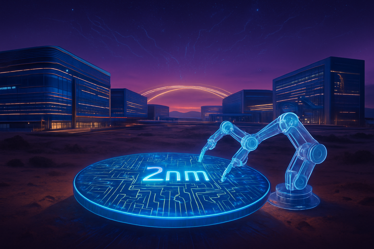
    Innovations poised to reshape the tech industry in the near future include wide-bandgap (WBG) materials like Gallium Nitride (GaN) and Silicon Carbide (SiC), which offer superior electrical efficiency, higher electron mobility, and better heat resistance for high-power applications, critical for EVs, 5G infrastructure, and data centers. Complementing these are two-dimensional (2D) materials such as graphene and Molybdenum Disulfide (MoS2), providing pathways to extreme miniaturization, enhanced electrostatic control, and even flexible electronics due to their atomic thinness. Beyond current FinFET transistor designs, new architectures like Gate-All-Around FETs (GAA-FETs, including nanosheets and nanoribbons) and Complementary FETs (CFETs) are becoming critical, enabling superior channel control and denser, more energy-efficient chips required for next-generation logic at 2nm nodes and beyond. Furthermore, advanced packaging techniques like chiplets and 3D stacking, along with the integration of silicon photonics for faster data transmission, are becoming essential to overcome bandwidth limitations and reduce energy consumption in high-performance computing and AI workloads. These advancements are not merely incremental improvements; they represent a fundamental re-evaluation of foundational materials and structures, enabling entirely new classes of AI applications, neuromorphic computing, and specialized processing that will power the next wave of technological innovation.

    The Technical Core: Unpacking the Next-Gen Semiconductor Innovations

    The semiconductor industry is undergoing a profound transformation driven by the escalating demands for higher performance, greater energy efficiency, and miniaturization beyond the limits of traditional silicon-based architectures. Emerging semiconductor technologies, encompassing novel materials, advanced transistor designs, and innovative packaging techniques, are poised to reshape the tech industry, particularly in the realm of artificial intelligence (AI).

    Wide-Bandgap Materials: Gallium Nitride (GaN) and Silicon Carbide (SiC)

    Gallium Nitride (GaN) and Silicon Carbide (SiC) are wide-bandgap (WBG) semiconductors that offer significant advantages over conventional silicon, especially in power electronics and high-frequency applications. Silicon has a bandgap of approximately 1.1 eV, while SiC boasts about 3.3 eV and GaN an even wider 3.4 eV. This larger energy difference allows WBG materials to sustain much higher electric fields before breakdown, handling nearly ten times higher voltages and operating at significantly higher temperatures (typically up to 200°C vs. silicon's 150°C). This improved thermal performance leads to better heat dissipation and allows for simpler, smaller, and lighter packaging. Both GaN and SiC exhibit higher electron mobility and saturation velocity, enabling switching frequencies up to 10 times higher than silicon, resulting in lower conduction and switching losses and efficiency improvements of up to 70%.

    While both offer significant improvements, GaN and SiC serve different power applications. SiC devices typically withstand higher voltages (1200V and above) and higher current-carrying capabilities, making them ideal for high-power applications such as automotive and locomotive traction inverters, large solar farms, and three-phase grid converters. GaN excels in high-frequency applications and lower power levels (up to a few kilowatts), offering superior switching speeds and lower losses, suitable for DC-DC converters and voltage regulators in consumer electronics and advanced computing.

    2D Materials: Graphene and Molybdenum Disulfide (MoS₂)

    Two-dimensional (2D) materials, only a few atoms thick, present unique properties for next-generation electronics. Graphene, a semimetal with a zero-electron bandgap, exhibits exceptional electrical and thermal conductivity, mechanical strength, flexibility, and optical transparency. Its high conductivity makes it promising for transparent conductive oxides and interconnects. However, its zero bandgap restricts its direct application in optoelectronics and field-effect transistors where a clear on/off switching characteristic is required.

    Molybdenum Disulfide (MoS₂), a transition metal dichalcogenide (TMDC), has a direct bandgap of 1.8 eV in its monolayer form. Unlike graphene, MoS₂'s natural bandgap makes it highly suitable for applications requiring efficient light absorption and emission, such as photodetectors, LEDs, and solar cells. MoS₂ monolayers have shown strong performance in 5nm electronic devices, including 2D MoS₂-based field-effect transistors and highly efficient photodetectors. Integrating MoS₂ and graphene creates hybrid systems that leverage the strengths of both, for instance, in high-efficiency solar cells or as ohmic contacts for MoS₂ transistors.

    Advanced Architectures: Gate-All-Around FETs (GAA-FETs) and Complementary FETs (CFETs)

    As traditional planar transistors reached their scaling limits, FinFETs emerged as 3D structures. FinFETs utilize a fin-shaped channel surrounded by the gate on three sides, offering improved electrostatic control and reduced leakage. However, at 3nm and below, FinFETs face challenges due to increasing variability and limitations in scaling metal pitch.

    Gate-All-Around FETs (GAA-FETs) overcome these limitations by having the gate fully enclose the entire channel on all four sides, providing superior electrostatic control and significantly reducing leakage and short-channel effects. GAA-FETs, typically constructed using stacked nanosheets, allow for a vertical form factor and continuous variation of channel width, offering greater design flexibility and improved drive current. They are emerging at 3nm and are expected to be dominant at 2nm and below.

    Complementary FETs (CFETs) are a potential future evolution beyond GAA-FETs, expected beyond 2030. CFETs dramatically reduce the footprint area by vertically stacking n-type MOSFET (nMOS) and p-type MOSFET (pMOS) transistors, allowing for much higher transistor density and promising significant improvements in power, performance, and area (PPA).

    Advanced Packaging: Chiplets, 3D Stacking, and Silicon Photonics

    Advanced packaging techniques are critical for continuing performance scaling as Moore's Law slows down, enabling heterogeneous integration and specialized functionalities, especially for AI workloads.

    Chiplets are small, specialized dies manufactured using optimal process nodes for their specific function. Multiple chiplets are assembled into a multi-chiplet module (MCM) or System-in-Package (SiP). This modular approach significantly improves manufacturing yields, allows for heterogeneous integration, and can lead to 30-40% lower energy consumption. It also optimizes cost by using cutting-edge nodes only where necessary.

    3D stacking involves vertically integrating multiple semiconductor dies or wafers using Through-Silicon Vias (TSVs) for vertical electrical connections. This dramatically shortens interconnect distances. 2.5D packaging places components side-by-side on an interposer, increasing bandwidth and reducing latency. True 3D packaging stacks active dies vertically using hybrid bonding, achieving even greater integration density, higher I/O density, reduced signal propagation delays, and significantly lower latency. These solutions can reduce system size by up to 70% and improve overall computing performance by up to 10 times.

    Silicon photonics integrates optical and electronic components on a single silicon chip, using light (photons) instead of electrons for data transmission. This enables extremely high bandwidth and low power consumption. In AI, silicon photonics, particularly through Co-Packaged Optics (CPO), is replacing copper interconnects to reduce power and latency in multi-rack AI clusters and data centers, addressing bandwidth bottlenecks for high-performance AI systems.

    Initial Reactions from the AI Research Community and Industry Experts

    The AI research community and industry experts have shown overwhelmingly positive reactions to these emerging semiconductor technologies. They are recognized as critical for fueling the next wave of AI innovation, especially given AI's increasing demand for computational power, vast memory bandwidth, and ultra-low latency. Experts acknowledge that traditional silicon scaling (Moore's Law) is reaching its physical limits, making advanced packaging techniques like 3D stacking and chiplets crucial solutions. These innovations are expected to profoundly impact various sectors, including autonomous vehicles, IoT, 5G/6G networks, cloud computing, and advanced robotics. Furthermore, AI itself is not only a consumer but also a catalyst for innovation in semiconductor design and manufacturing, with AI algorithms accelerating material discovery, speeding up design cycles, and optimizing power efficiency.

    Corporate Battlegrounds: How Emerging Semiconductors Reshape the Tech Industry

    The rapid evolution of Artificial Intelligence (AI) is heavily reliant on breakthroughs in semiconductor technology. Emerging technologies like wide-bandgap materials, 2D materials, Gate-All-Around FETs (GAA-FETs), Complementary FETs (CFETs), chiplets, 3D stacking, and silicon photonics are reshaping the landscape for AI companies, tech giants, and startups by offering enhanced performance, power efficiency, and new capabilities.

    Wide-Bandgap Materials: Powering the AI Infrastructure

    WBG materials (GaN, SiC) are crucial for power management in energy-intensive AI data centers, allowing for more efficient power delivery to AI accelerators and reducing operational costs. Companies like Nvidia (NASDAQ: NVDA) are already partnering to deploy GaN in 800V HVDC architectures for their next-generation AI processors. Tech giants like Google (NASDAQ: GOOGL), Meta (NASDAQ: META), and AMD (NASDAQ: AMD) will be major consumers for their custom silicon. Navitas Semiconductor (NASDAQ: NVTS) is a key beneficiary, validated as a critical supplier for AI infrastructure through its partnership with Nvidia. Other players like Wolfspeed (NYSE: WOLF), Infineon Technologies (FWB: IFX) (which acquired GaN Systems), ON Semiconductor (NASDAQ: ON), and STMicroelectronics (NYSE: STM) are solidifying their positions. Companies embracing WBG materials will have more energy-efficient and powerful AI systems, displacing silicon in power electronics and RF applications.

    2D Materials: Miniaturization and Novel Architectures

    2D materials (graphene, MoS2) promise extreme miniaturization, enabling ultra-low-power, high-density computing and in-sensor memory for AI. Major foundries like TSMC (NYSE: TSM) and Intel (NASDAQ: INTC) are heavily investing in their research and integration. Startups like Graphenea and Haydale Graphene Industries specialize in producing these nanomaterials. Companies successfully integrating 2D materials for ultra-fast, energy-efficient transistors will gain significant market advantages, although these are a long-term solution to scaling limits.

    Advanced Transistor Architectures: The Core of Future Chips

    GAA-FETs and CFETs are critical for continuing miniaturization and enhancing the performance and power efficiency of AI processors. Foundries like TSMC, Samsung (KRX: 005930), and Intel are at the forefront of developing and implementing these, making their ability to master these nodes a key competitive differentiator. Tech giants designing custom AI chips will leverage these advanced nodes. Startups may face high entry barriers due to R&D costs, but advanced EDA tools from companies like Siemens (FWB: SIE) and Synopsys (NASDAQ: SNPS) will be crucial. Foundries that successfully implement these earliest will attract top AI chip designers.

    Chiplets: Modular Innovation for AI

    Chiplets enable the creation of highly customized, powerful, and energy-efficient AI accelerators by integrating diverse, purpose-built processing units. This modular approach optimizes cost and improves energy efficiency. Tech giants like Google, Amazon (NASDAQ: AMZN), and Microsoft (NASDAQ: MSFT) are heavily reliant on chiplets for their custom AI chips. AMD has been a pioneer, and Intel is heavily invested with its IDM 2.0 strategy. Broadcom (NASDAQ: AVGO) is also developing 3.5D packaging. Chiplets significantly lower the barrier to entry for specialized AI hardware development for startups. This technology fosters an "infrastructure arms race," challenging existing monopolies like Nvidia's dominance.

    3D Stacking: Overcoming the Memory Wall

    3D stacking vertically integrates multiple layers of chips to enhance performance, reduce power, and increase storage capacity. This, especially with High Bandwidth Memory (HBM), is critical for AI accelerators, dramatically increasing bandwidth between processing units and memory. AMD (Instinct MI300 series), Intel (Foveros), Nvidia, Samsung, Micron (NASDAQ: MU), and SK Hynix (KRX: 000660) are heavily investing in this. Foundries like TSMC, Intel, and Samsung are making massive investments in advanced packaging, with TSMC dominating. Companies like Micron are becoming key memory suppliers for AI workloads. This is a foundational enabler for sustaining AI innovation beyond Moore's Law.

    Silicon Photonics: Ultra-Fast, Low-Power Interconnects

    Silicon photonics uses light for data transmission, enabling high-speed, low-power communication. This directly addresses the "bandwidth wall" for real-time AI processing and large language models. Tech giants like Google, Amazon, and Microsoft, invested in cloud AI services, benefit immensely for their data center interconnects. Startups focusing on optical I/O chiplets, like Ayar Labs, are emerging as leaders. Silicon photonics is positioned to solve the "twin crises" of power consumption and bandwidth limitations in AI, transforming the switching layer in AI networks.

    Overall Competitive Implications and Disruption

    The competitive landscape is being reshaped by an "infrastructure arms race" driven by advanced packaging and chiplet integration, challenging existing monopolies. Tech giants are increasingly designing their own custom AI chips, directly challenging general-purpose GPU providers. A severe talent shortage in semiconductor design and manufacturing is exacerbating competition for specialized talent. The industry is shifting from monolithic to modular chip designs, and the energy efficiency imperative is pushing existing inefficient products towards obsolescence. Foundries (TSMC, Intel Foundry Services, Samsung Foundry) and companies providing EDA tools (Arm (NASDAQ: ARM) for architectures, Siemens, Synopsys, Cadence (NASDAQ: CDNS)) are crucial. Memory innovators like Micron and SK Hynix are critical, and strategic partnerships are vital for accelerating adoption.

    The Broader Canvas: AI's Symbiotic Dance with Advanced Semiconductors

    Emerging semiconductor technologies are fundamentally reshaping the landscape of artificial intelligence, enabling unprecedented computational power, efficiency, and new application possibilities. These advancements are critical for overcoming the physical and economic limitations of traditional silicon-based architectures and fueling the current "AI Supercycle."

    Fitting into the Broader AI Landscape

    The relationship between AI and semiconductors is deeply symbiotic. AI's explosive growth, especially in generative AI and large language models (LLMs), is the primary catalyst driving unprecedented demand for smaller, faster, and more energy-efficient semiconductors. These emerging technologies are the engine powering the next generation of AI, enabling capabilities that would be impossible with traditional silicon. They fit into several key AI trends:

    • Beyond Moore's Law: As traditional transistor scaling slows, these technologies, particularly chiplets and 3D stacking, provide alternative pathways to continued performance gains.

    • Heterogeneous Computing: Combining different processor types with specialized memory and interconnects is crucial for optimizing diverse AI workloads, and emerging semiconductors enable this more effectively.

    • Energy Efficiency: The immense power consumption of AI necessitates hardware innovations that significantly improve energy efficiency, directly addressed by wide-bandbandgap materials and silicon photonics.

    • Memory Wall Breakthroughs: AI workloads are increasingly memory-bound. 3D stacking with HBM is directly addressing the "memory wall" by providing massive bandwidth, critical for LLMs.

    • Edge AI: The demand for real-time AI processing on devices with minimal power consumption drives the need for optimized chips using these advanced materials and packaging techniques.

    • AI for Semiconductors (AI4EDA): AI is not just a consumer but also a powerful tool in the design, manufacturing, and optimization of semiconductors themselves, creating a powerful feedback loop.

    Impacts and Potential Concerns

    Positive Impacts: These innovations deliver unprecedented performance, significantly faster processing, higher data throughput, and lower latency, directly translating to more powerful and capable AI models. They bring enhanced energy efficiency, greater customization and flexibility through chiplets, and miniaturization for widespread AI deployment. They also open new AI frontiers like neuromorphic computing and quantum AI, driving economic growth.

    Potential Concerns: The exorbitant costs of innovation, requiring billions in R&D and state-of-the-art fabrication facilities, create high barriers to entry. Physical and engineering challenges, such as heat dissipation and managing complexity at nanometer scales, remain difficult. Supply chain vulnerability, due to extreme concentration of advanced manufacturing, creates geopolitical risks. Data scarcity for AI in manufacturing, and integration/compatibility issues with new hardware architectures, also pose hurdles. Despite efficiency gains, the sheer scale of AI models means overall electricity consumption for AI is projected to rise dramatically, posing a significant sustainability challenge. Ethical concerns about workforce disruption, privacy, bias, and misuse of AI also become more pressing.

    Comparison to Previous AI Milestones

    The current advancements are ushering in an "AI Supercycle" comparable to previous transformative periods. Unlike past milestones often driven by software on existing hardware, this era is defined by deep co-design between AI algorithms and specialized hardware, representing a more profound shift. The relationship is deeply symbiotic, with AI driving hardware innovation and vice versa. These technologies are directly tackling fundamental physical and architectural bottlenecks (Moore's Law limits, memory wall, power consumption) that previous generations faced. The trend is towards highly specialized AI accelerators, often enabled by chiplets and 3D stacking, leading to unprecedented efficiency. The scale of modern AI is vastly greater, necessitating these innovations. A distinct difference is the emergence of AI being used to accelerate semiconductor development and manufacturing itself.

    The Horizon: Charting the Future of Semiconductor Innovation

    Emerging semiconductor technologies are rapidly advancing to meet the escalating demand for more powerful, energy-efficient, and compact electronic devices. These innovations are critical for driving progress in fields like artificial intelligence (AI), automotive, 5G/6G communication, and high-performance computing (HPC).

    Wide-Bandgap Materials (SiC and GaN)

    Near-Term (1-5 years): Continued optimization of manufacturing processes for SiC and GaN, increasing wafer sizes (e.g., to 200mm SiC wafers), and reducing production costs will enable broader adoption. SiC is expected to gain significant market share in EVs, power electronics, and renewable energy.
    Long-Term (Beyond 5 years): WBG semiconductors, including SiC and GaN, will largely replace traditional silicon in power electronics. Further integration with advanced packaging will maximize performance. Diamond (Dia) is emerging as a future ultrawide bandgap semiconductor.
    Applications: EVs (inverters, motor drives, fast charging), 5G/6G infrastructure, renewable energy systems, data centers, industrial power conversion, aerospace, and consumer electronics (fast chargers).
    Challenges: High production costs, material quality and reliability, lack of standardized norms, and limited production capabilities.
    Expert Predictions: SiC will become indispensable for electrification. The WBG technology market is expected to boom, projected to reach around $24.5 billion by 2034.

    2D Materials

    Near-Term (1-5 years): Continued R&D, with early adopters implementing them in niche applications. Hybrid approaches with silicon or WBG semiconductors might be initial commercialization pathways. Graphene is already used in thermal management.
    Long-Term (Beyond 5 years): 2D materials are expected to become standard components in high-performance and next-generation devices, enabling ultra-dense, energy-efficient transistors at atomic scales and monolithic 3D integration. They are crucial for logic applications.
    Applications: Ultra-fast, energy-efficient chips (graphene as optical-electronic translator), advanced transistors (MoS2, InSe), flexible and wearable electronics, high-performance sensors, neuromorphic computing, thermal management, and quantum photonics.
    Challenges: Scalability of high-quality production, compatible fabrication techniques, material stability (degradation by moisture/oxygen), cost, and integration with silicon.
    Expert Predictions: Crucial for future IT, enabling breakthroughs in device performance. The global 2D materials market is projected to reach $4,000 million by 2031, growing at a CAGR of 25.3%.

    Gate-All-Around FETs (GAA-FETs) and Complementary FETs (CFETs)

    Near-Term (1-5 years): GAA-FETs are critical for shrinking transistors beyond 3nm and 2nm nodes, offering superior electrostatic control and reduced leakage. The industry is transitioning to GAA-FETs.
    Long-Term (Beyond 5 years): Exploration of innovative designs like U-shaped FETs and CFETs as successors. CFETs are expected to offer even greater density and efficiency by vertically stacking n-type and p-type GAA-FETs. Research into alternative materials for channels is also on the horizon.
    Applications: HPC, AI processors, low-power logic systems, mobile devices, and IoT.
    Challenges: Fabrication complexities, heat dissipation, leakage currents, material compatibility, and scalability issues.
    Expert Predictions: GAA-FETs are pivotal for future semiconductor technologies, particularly for low-power logic systems, HPC, and AI domains.

    Chiplets

    Near-Term (1-5 years): Broader adoption beyond high-end CPUs and GPUs. The Universal Chiplet Interconnect Express (UCIe) standard is expected to mature, fostering a robust ecosystem. Advanced packaging (2.5D, 3D hybrid bonding) will become standard for HPC and AI, alongside intensified adoption of HBM4.
    Long-Term (Beyond 5 years): Fully modular semiconductor designs with custom chiplets optimized for specific AI workloads will dominate. Transition from 2.5D to more prevalent 3D heterogeneous computing. Co-packaged optics (CPO) are expected to replace traditional copper interconnects.
    Applications: HPC and AI hardware (specialized accelerators, breaking memory wall), CPUs and GPUs, data centers, autonomous vehicles, networking, edge computing, and smartphones.
    Challenges: Standardization (UCIe addressing this), complex thermal management, robust testing methodologies for multi-vendor ecosystems, design complexity, packaging/interconnect technology, and supply chain coordination.
    Expert Predictions: Chiplets will be found in almost all high-performance computing systems, becoming ubiquitous in AI hardware. The global chiplet market is projected to reach hundreds of billions of dollars.

    3D Stacking

    Near-Term (1-5 years): Rapid growth driven by demand for enhanced performance. TSMC (NYSE: TSM), Samsung, and Intel are leading this trend. Quick move towards glass substrates to replace current 2.5D and 3D packaging between 2026 and 2030.
    Long-Term (Beyond 5 years): Increasingly prevalent for heterogeneous computing, integrating different functional layers directly on a single chip. Further miniaturization and integration with quantum computing and photonics. More cost-effective solutions.
    Applications: HPC and AI (higher memory density, high-performance memory, quantum-optimized logic), mobile devices and wearables, data centers, consumer electronics, and automotive.
    Challenges: High manufacturing complexity, thermal management, yield challenges, high cost, interconnect technology, and supply chain.
    Expert Predictions: Rapid growth in the 3D stacking market, with projections ranging from reaching USD 9.48 billion by 2033 to USD 3.1 billion by 2028.

    Silicon Photonics

    Near-Term (1-5 years): Robust growth driven by AI and datacom transceiver demand. Arrival of 3.2Tbps transceivers by 2026. Innovation will involve monolithic integration using quantum dot lasers.
    Long-Term (Beyond 5 years): Pivotal role in next-generation computing, with applications in high-bandwidth chip-to-chip interconnects, advanced packaging, and co-packaged optics (CPO) replacing copper. Programmable photonics and photonic quantum computers.
    Applications: AI data centers, telecommunications, optical interconnects, quantum computing, LiDAR systems, healthcare sensors, photonic engines, and data storage.
    Challenges: Material limitations (achieving optical gain/lasing in silicon), integration complexity (high-powered lasers), cost management, thermal effects, lack of global standards, and production lead times.
    Expert Predictions: Market projected to grow significantly (44-45% CAGR between 2022-2028/2029). AI is a major driver. Key players will emerge, and China is making strides towards global leadership.

    The AI Supercycle: A Comprehensive Wrap-Up of Semiconductor's New Era

    Emerging semiconductor technologies are rapidly reshaping the landscape of modern computing and artificial intelligence, driving unprecedented innovation and projected market growth to a trillion dollars by the end of the decade. This transformation is marked by advancements across materials, architectures, packaging, and specialized processing units, all converging to meet the escalating demands for faster, more efficient, and intelligent systems.

    Key Takeaways

    The core of this revolution lies in several synergistic advancements: advanced transistor architectures like GAA-FETs and the upcoming CFETs, pushing density and efficiency beyond FinFETs; new materials such as Gallium Nitride (GaN) and Silicon Carbide (SiC), which offer superior power efficiency and thermal performance for demanding applications; and advanced packaging technologies including 2.5D/3D stacking and chiplets, enabling heterogeneous integration and overcoming traditional scaling limits by creating modular, highly customized systems. Crucially, specialized AI hardware—from advanced GPUs to neuromorphic chips—is being developed with these technologies to handle complex AI workloads. Furthermore, quantum computing, though nascent, leverages semiconductor breakthroughs to explore entirely new computational paradigms. The Universal Chiplet Interconnect Express (UCIe) standard is rapidly maturing to foster interoperability in the chiplet ecosystem, and High Bandwidth Memory (HBM) is becoming the "scarce currency of AI," with HBM4 pushing the boundaries of data transfer speeds.

    Significance in AI History

    Semiconductors have always been the bedrock of technological progress. In the context of AI, these emerging technologies mark a pivotal moment, driving an "AI Supercycle." They are not just enabling incremental gains but are fundamentally accelerating AI capabilities, pushing beyond the limits of Moore's Law through innovative architectural and packaging solutions. This era is characterized by a deep hardware-software symbiosis, where AI's immense computational demands directly fuel semiconductor innovation, and in turn, these hardware advancements unlock new AI models and applications. This also facilitates the democratization of AI, allowing complex models to run on smaller, more accessible edge devices. The intertwining evolution is so profound that AI is now being used to optimize semiconductor design and manufacturing itself.

    Long-Term Impact

    The long-term impact of these emerging semiconductor technologies will be transformative, leading to ubiquitous AI seamlessly integrated into every facet of life, from smart cities to personalized healthcare. A strong focus on energy efficiency and sustainability will intensify, driven by materials like GaN and SiC and eco-friendly production methods. Geopolitical factors will continue to reshape global supply chains, fostering more resilient and regionally focused manufacturing. New frontiers in computing, particularly quantum AI, promise to tackle currently intractable problems. Finally, enhanced customization and functionality through advanced packaging will broaden the scope of electronic devices across various industrial applications. The transition to glass substrates for advanced packaging between 2026 and 2030 is also a significant long-term shift to watch.

    What to Watch For in the Coming Weeks and Months

    The semiconductor landscape remains highly dynamic. Key areas to monitor include:

    • Manufacturing Process Node Updates: Keep a close eye on progress in the 2nm race and Angstrom-class (1.6nm, 1.8nm) technologies from leading foundries like TSMC (NYSE: TSM) and Intel (NASDAQ: INTC), focusing on their High Volume Manufacturing (HVM) timelines and architectural innovations like backside power delivery.
    • Advanced Packaging Capacity Expansion: Observe the aggressive expansion of advanced packaging solutions, such as TSMC's CoWoS and other 3D IC technologies, which are crucial for next-generation AI accelerators.
    • HBM Developments: High Bandwidth Memory remains critical. Watch for updates on new HBM generations (e.g., HBM4), customization efforts, and its increasing share of the DRAM market, with revenue projected to double in 2025.
    • AI PC and GenAI Smartphone Rollouts: The proliferation of AI-capable PCs and GenAI smartphones, driven by initiatives like Microsoft's (NASDAQ: MSFT) Copilot+ baseline, represents a substantial market shift for edge AI processors.
    • Government Incentives and Supply Chain Shifts: Monitor the impact of government incentives like the US CHIPS and Science Act, as investments in domestic manufacturing are expected to become more evident from 2025, reshaping global supply chains.
    • Neuromorphic Computing Progress: Look for breakthroughs and increased investment in neuromorphic chips that mimic brain-like functions, promising more energy-efficient and adaptive AI at the edge.

    The industry's ability to navigate the complexities of miniaturization, thermal management, power consumption, and geopolitical influences will determine the pace and direction of future innovations.


    This content is intended for informational purposes only and represents analysis of current AI developments.

    TokenRing AI delivers enterprise-grade solutions for multi-agent AI workflow orchestration, AI-powered development tools, and seamless remote collaboration platforms. For more information, visit https://www.tokenring.ai/.

  • Silicon’s Unyielding Ascent: How AI Fuels Semiconductor Resilience Amidst Economic Headwinds

    Silicon’s Unyielding Ascent: How AI Fuels Semiconductor Resilience Amidst Economic Headwinds

    October 6, 2025 – The semiconductor sector is demonstrating unprecedented resilience and robust growth, primarily propelled by the insatiable demand for Artificial Intelligence (AI) and high-performance computing (HPC). This formidable strength persists even as the broader economy, reflected in the S&P 500, navigates uncertainties like an ongoing U.S. government shutdown. The industry, projected to reach nearly $700 billion in global sales this year with an anticipated 11% growth, remains a powerful engine of technological advancement and a significant driver of market performance.

    The immediate significance of this resilience is profound. The semiconductor industry, particularly AI-centric companies, is a leading force in driving market momentum. Strategic partnerships, such as OpenAI's recent commitment to massive chip purchases from AMD, underscore the critical role semiconductors play in advancing AI and reshaping the tech landscape, solidifying the sector as the bedrock of modern technological advancement.

    The AI Supercycle: Technical Underpinnings of Semiconductor Strength

    The semiconductor industry is undergoing a profound transformation, often termed the "AI Supercycle," where AI not only fuels unprecedented demand for advanced chips but also actively participates in their design and manufacturing. This symbiotic relationship is crucial for enhancing resilience, improving efficiency, and accelerating innovation across the entire value chain. AI-driven solutions are dramatically reducing chip design cycles, optimizing circuit layouts, and rigorously enhancing verification and testing to detect design flaws with unprecedented accuracy, with companies like Synopsys reporting a 75% reduction in design timelines.

    In fabrication plants, AI and Machine Learning (ML) are game-changers for yield optimization. They enable predictive maintenance to avert costly downtime, facilitate real-time process adjustments for higher precision, and employ advanced defect detection systems. For example, TSMC (NYSE: TSM) has boosted its 3nm production line yields by 20% through AI-driven defect detection. NVIDIA's (NASDAQ: NVDA) NV-Tesseract and NIM technologies further enhance anomaly detection in fabs, minimizing production losses. This AI integration extends to supply chain optimization, achieving over 90% demand forecasting accuracy and reducing inventory holding costs by 15-20% by incorporating global economic indicators and real-time consumer behavior.

    The relentless demands of AI workloads necessitate immense computational power, vast memory bandwidth, and ultra-low latency, driving the development of specialized chip architectures far beyond traditional CPUs. Current leading AI chips include NVIDIA's Blackwell Ultra GPU (expected H2 2025) with 288 GB HBM3e and enhanced FP4 inference, and AMD's (NASDAQ: AMD) Instinct MI300 series, featuring the MI325X with 256 GB HBM3E and 6 TB/s bandwidth, offering 6.8x AI training performance over its predecessor. Intel's (NASDAQ: INTC) Gaudi 3 AI Accelerator, fabricated on TSMC's 5nm process, boasts 128 GB HBM2e with 3.7 TB/s bandwidth and 1.8 PFLOPs of FP8 and BF16 compute power, claiming significant performance and power efficiency gains over NVIDIA's H100 on certain models. High-Bandwidth Memory (HBM), including HBM3e and the upcoming HBM4, is critical, with SK hynix sampling 16-Hi HBM3e chips in 2025.

    These advancements differ significantly from previous approaches through specialization (purpose-built ASICs, NPUs, and highly optimized GPUs), advanced memory architecture (HBM), fine-grained precision support (INT8, FP8), and sophisticated packaging technologies like chiplets and CoWoS. The active role of AI in design and manufacturing, creating a self-reinforcing cycle, fundamentally shifts the innovation paradigm. The AI research community and industry experts overwhelmingly view AI as an "indispensable tool" and a "game-changer," recognizing an "AI Supercycle" driving unprecedented market growth, with AI chips alone projected to exceed $150 billion in sales in 2025. However, a "precision shortage" of advanced AI chips, particularly in sub-11nm geometries and advanced packaging, persists as a key bottleneck.

    Corporate Beneficiaries and Competitive Dynamics

    The AI-driven semiconductor resilience is creating clear winners and intensifying competition among tech giants and specialized chipmakers.

    NVIDIA (NASDAQ: NVDA) remains the undisputed market leader and primary beneficiary, with its market capitalization soaring past $4.5 trillion. The company commands an estimated 70-80% market share in new AI data center spending, with its GPUs being indispensable for AI model training. NVIDIA's integrated hardware and software ecosystem, particularly its CUDA platform, provides a significant competitive moat. Data center AI revenue is projected to reach $172 billion by 2025, with its AI PC business also experiencing rapid growth.

    Advanced Micro Devices (NASDAQ: AMD) is rapidly emerging as NVIDIA's chief competitor. A monumental strategic partnership with OpenAI, announced in October 2025, involves deploying up to 6 gigawatts of AMD Instinct GPUs for next-generation AI infrastructure. This focus on inference workloads and strong partnerships could position AMD to capture 15-20% of the estimated $165 billion AI chip market by 2030, with $3.5 billion in AI accelerator orders for 2025.

    Intel (NASDAQ: INTC), while facing challenges in the high-end AI chip market, is pursuing its IDM 2.0 strategy and benefiting from U.S. CHIPS Act funding. Intel aims to deliver full-stack AI solutions and targets the growing edge AI market. A strategic development includes NVIDIA's $5 billion investment in Intel stock, with Intel building NVIDIA-custom x86 CPUs for AI infrastructure. TSMC (NYSE: TSM) is the critical foundational partner, manufacturing chips for NVIDIA, AMD, Apple (NASDAQ: AAPL), Qualcomm (NASDAQ: QCOM), and Broadcom (NASDAQ: AVGO). Its revenue surged over 40% year-over-year in early 2025, with AI applications driving 60% of its Q2 2025 revenue. Samsung Electronics (KRX: 005930) is aggressively expanding its foundry business, positioning itself as a "one-stop shop" for AI chip development by integrating memory, foundry services, and advanced packaging.

    Hyperscalers like Google (NASDAQ: GOOGL), Microsoft (NASDAQ: MSFT), and Amazon (NASDAQ: AMZN) are central to the AI boom, with their collective annual investment in AI infrastructure projected to triple to $450 billion by 2027. Microsoft is seeing significant AI monetization, with AI-driven revenue up 175% year-over-year. However, Microsoft has adjusted its internal AI chip roadmap, highlighting challenges in competing with industry leaders. Broadcom (NASDAQ: AVGO) and Marvell Technology (NASDAQ: MRVL) are also key beneficiaries, with AI sales surging for Broadcom, partly due to a $10 billion custom chip order linked to OpenAI. AI is expected to account for 40-50% of revenue for both companies. The competitive landscape is also shaped by the rise of custom silicon, foundry criticality, memory innovation, and the importance of software ecosystems.

    Broader Implications and Geopolitical Undercurrents

    The AI-driven semiconductor resilience extends far beyond corporate balance sheets, profoundly impacting the broader AI landscape, geopolitical stability, and even environmental considerations. The "AI Supercycle" signifies a fundamental reshaping of the technological landscape, where generative AI, HPC, and edge AI are driving exponential demand for specialized silicon across every sector. The global semiconductor market is projected to reach approximately $800 billion in 2025, on track for a $1 trillion industry by 2030.

    The economic impact is significant, with increased profitability for companies with AI exposure and a reshaping of global supply chain strategies. Technologically, AI is accelerating chip design, cutting timelines from months to weeks, and enabling the creation of more efficient and innovative chip designs, including the exploration of neuromorphic and quantum computing. Societally, the pervasive integration of AI-enabled semiconductors is driving innovation across industries, from AI-powered consumer devices to advanced diagnostics in healthcare and autonomous systems.

    However, this rapid advancement is not without its concerns. Intense geopolitical competition, particularly between the United States and China, is a major concern. Export controls, trade restrictions, and substantial investments in domestic semiconductor production globally highlight the strategic importance of this sector. The high concentration of advanced chip manufacturing in Taiwan (TSMC) and South Korea (Samsung) creates significant vulnerabilities and strategic chokepoints, making the supply chain susceptible to disruptions and driving "technonationalism." Environmental concerns also loom large, as the production of AI chips is extremely energy and water-intensive, leading to substantial carbon emissions and a projected 3% contribution to total global emissions by 2040 if current trends persist. A severe global talent shortage further threatens sustained progress.

    Compared to previous AI milestones, the current "AI Supercycle" represents a distinct phase. Unlike the broad pandemic-era chip shortage, the current constraints are highly concentrated on advanced AI chips and their cutting-edge manufacturing processes. This era elevates semiconductor supply chain resilience from a niche industry concern to an urgent, strategic imperative, directly impacting national security and a nation's capacity for AI leadership, a level of geopolitical tension and investment arguably unprecedented.

    The Road Ahead: Future Developments in Silicon and AI

    The AI-driven semiconductor market anticipates a sustained "supercycle" of expansion, with significant advancements expected in the near and long term, fundamentally transforming computing paradigms and AI integration.

    In the near term (2025-2027), the global AI chip market is projected for significant growth, with sales potentially reaching $700 billion in 2025. Mass production of 2nm chips is scheduled to begin in late 2025, followed by A16 (1.6nm) for data center AI and HPC by late 2026. Demand for HBM, including HBM3E and HBM4, is skyrocketing, with Samsung accelerating its HBM4 development for completion by H2 2025. There's a strong trend towards custom AI chips developed by hyperscalers and enterprises, and Edge AI is gaining significant traction with AI-enabled PCs and mobile devices expanding rapidly.

    Longer term (2028-2035 and beyond), the global semiconductor market is projected to reach $1 trillion by 2030, with the AI chip market potentially exceeding $400 billion by 2030. The roadmap includes A14 (1.4nm) for mass production in 2028. Beyond traditional silicon, emerging architectures like neuromorphic computing, photonic computing (expected commercial viability by 2028), and quantum computing are poised to offer exponential leaps in efficiency and speed. TSMC forecasts a proliferation of "physical AI," with 1.3 billion AI robots globally by 2035, necessitating pushing AI capabilities to every edge device. This will be accompanied by an unprecedented expansion of fabrication capacity, with 105 new fabs expected to come online through 2028, and nearshoring efforts maturing between 2027 and 2029.

    Potential applications are vast, spanning data centers and cloud computing, edge AI (autonomous vehicles, industrial automation, AR, IoT, AI-enabled PCs/smartphones), healthcare (diagnostics, personalized treatment), manufacturing, energy management, defense, and more powerful generative AI models. However, significant challenges remain, including technical hurdles like heat dissipation, memory bandwidth, and design complexity at nanometer scales. Economic challenges include the astronomical costs of fabs and R&D, supply chain vulnerabilities, and the massive energy consumption of AI. Geopolitical and regulatory challenges, along with a severe talent shortage, also need addressing. Experts predict sustained growth, market dominance by AI chips, pervasive AI impact (transforming 40% of daily work tasks by 2028), and continued innovation in architectures, including "Sovereign AI" initiatives by governments.

    A New Era of Silicon Dominance

    The AI-driven semiconductor market is navigating a period of intense growth and transformation, exhibiting significant resilience driven by insatiable AI demand. This "AI Supercycle" marks a pivotal moment in AI history, fundamentally reshaping the technological landscape and positioning the semiconductor industry at the core of the digital economy's evolution. The industry's ability to overcome persistent supply chain fragilities, geopolitical pressures, and talent shortages through strategic innovation and diversification will define its long-term impact on AI's trajectory and the global technological landscape.

    Key takeaways include the projected growth towards a $1 trillion market by 2030, the targeted scarcity of advanced AI chips, escalating geopolitical tensions driving regionalized manufacturing, and the critical global talent shortage. AI itself has become an indispensable tool for enhancing chip design, manufacturing, and supply chain management, creating a virtuous cycle of innovation. While economic benefits are heavily concentrated among a few leading companies, the long-term impact promises transformative advancements in materials, architectures, and energy-efficient solutions. However, concerns about market overvaluation, ethical AI deployment, and the physical limits of transistor scaling remain pertinent.

    In the coming weeks and months, watch for the ramp-up of 2nm and 3nm chip production, expansion of advanced packaging capacity, and the market reception of AI-enabled consumer electronics. Further geopolitical developments and strategic alliances, particularly around securing chip allocations and co-development, will be crucial. Monitor talent development initiatives and how competitors continue to challenge NVIDIA's dominance. Finally, keep an eye on innovations emphasizing energy-efficient chip designs and improved thermal management solutions as the immense power demands of AI continue to grow.


    This content is intended for informational purposes only and represents analysis of current AI developments.

    TokenRing AI delivers enterprise-grade solutions for multi-agent AI workflow orchestration, AI-powered development tools, and seamless remote collaboration platforms.
    For more information, visit https://www.tokenring.ai/.

  • The New Era of Silicon: AI, Advanced Packaging, and Novel Materials Propel Chip Quality to Unprecedented Heights

    The New Era of Silicon: AI, Advanced Packaging, and Novel Materials Propel Chip Quality to Unprecedented Heights

    October 6, 2025 – The semiconductor industry is in the midst of a profound transformation, driven by an insatiable global demand for increasingly powerful, efficient, and reliable chips. This revolution, fueled by the synergistic advancements in Artificial Intelligence (AI), sophisticated packaging techniques, and the exploration of novel materials, is fundamentally reshaping the quality and capabilities of semiconductors across every application, from the smartphones in our pockets to the autonomous vehicles on our roads. As traditional transistor scaling faces physical limitations, these innovations are not merely extending Moore's Law but are ushering in a new era of chip design and manufacturing, crucial for the continued acceleration of AI and the broader digital economy.

    The immediate significance of these developments is palpable. The global semiconductor market is projected to reach an all-time high of $697 billion in 2025, with AI technologies alone expected to account for over $150 billion in sales. This surge is a direct reflection of the breakthroughs in chip quality, which are enabling faster innovation cycles, expanding the possibilities for new applications, and ensuring the reliability and security of critical systems in an increasingly interconnected world. The industry is witnessing a shift where quality, driven by intelligent design and manufacturing, is as critical as raw performance.

    The Technical Core: AI, Advanced Packaging, and Materials Redefine Chip Excellence

    The current leap in semiconductor quality is underpinned by a trifecta of technical advancements, each pushing the boundaries of what's possible.

    AI's Intelligent Hand in Chipmaking: AI, particularly machine learning (ML) and deep learning (DL), has become an indispensable tool across the entire semiconductor lifecycle. In design, AI-powered Electronic Design Automation (EDA) tools, such as Synopsys' (NASDAQ: SNPS) DSO.ai system, are revolutionizing workflows by automating complex tasks like layout generation, design optimization, and defect prediction. This drastically reduces time-to-market; a 5nm chip's optimization cycle, for instance, has reportedly shrunk from six months to six weeks. AI can explore billions of possible transistor arrangements, creating designs that human engineers might not conceive, leading to up to a 40% reduction in power efficiency and a 3x to 5x improvement in design productivity. In manufacturing, AI algorithms analyze vast amounts of real-time production data to optimize processes, predict maintenance needs, and significantly reduce defect rates, boosting yield rates by up to 30% for advanced nodes. For quality control, AI, ML, and deep learning are integrated into visual inspection systems, achieving over 99% accuracy in detecting, classifying, and segmenting defects, even at submicron and nanometer scales. Purdue University's recent research, for example, integrates advanced imaging with AI to detect minuscule defects, moving beyond traditional manual inspections to ensure chip reliability and combat counterfeiting. This differs fundamentally from previous rule-based or human-intensive approaches, offering unprecedented precision and efficiency.

    Advanced Packaging: Beyond Moore's Law: As traditional transistor scaling slows, advanced packaging has emerged as a cornerstone of semiconductor innovation, enabling continued performance improvements and reduced power consumption. This involves combining multiple semiconductor chips (dies or chiplets) into a single electronic package, rather than relying on a single monolithic die. 2.5D and 3D-IC packaging are leading the charge. 2.5D places components side-by-side on an interposer, while 3D-IC vertically stacks active dies, often using through-silicon vias (TSVs) for ultra-short signal paths. Techniques like TSMC's (NYSE: TSM) CoWoS (chip-on-wafer-on-substrate) and Intel's (NASDAQ: INTC) EMIB (embedded multi-die interconnect bridge) exemplify this, achieving interconnection speeds of up to 4.8 TB/s (e.g., NVIDIA (NASDAQ: NVDA) Hopper H100 with HBM stacks). Hybrid bonding is crucial for advanced packaging, achieving interconnect pitches in the single-digit micrometer range, a significant improvement over conventional microbump technology (40-50 micrometers), and bandwidths up to 1000 GB/s. This allows for heterogeneous integration, where different chiplets (CPUs, GPUs, memory, specialized AI accelerators) are manufactured using their most suitable process nodes and then combined, optimizing overall system performance and efficiency. This approach fundamentally differs from traditional packaging, which typically packaged a single die and relied on slower PCB connections, offering increased functional density, reduced interconnect distances, and improved thermal management.

    Novel Materials: The Future Beyond Silicon: As silicon approaches its inherent physical limitations, novel materials are stepping in to redefine chip performance. Wide-Bandgap (WBG) Semiconductors like Gallium Nitride (GaN) and Silicon Carbide (SiC) are revolutionizing power electronics. GaN boasts a bandgap of 3.4 eV (compared to silicon's 1.1 eV) and a breakdown field strength ten times higher, allowing for 10-100 times faster switching speeds and operation at higher voltages and temperatures. SiC offers similar advantages with three times higher thermal conductivity than silicon, crucial for electric vehicles and industrial applications. Two-Dimensional (2D) Materials such as graphene and molybdenum disulfide (MoS₂) promise higher electron mobility (graphene can be 100 times greater than silicon) for faster switching and reduced power consumption, enabling extreme miniaturization. High-k Dielectrics, like Hafnium Oxide (HfO₂), replace silicon dioxide as gate dielectrics, significantly reducing gate leakage currents (by more than an order of magnitude) and power consumption in scaled transistors. These materials offer superior electrical, thermal, and scaling properties that silicon cannot match, opening doors for new device architectures and applications. The AI research community and industry experts have reacted overwhelmingly positively to these advancements, hailing AI as a "game-changer" for design and manufacturing, recognizing advanced packaging as a "critical enabler" for high-performance computing, and viewing novel materials as essential for overcoming silicon's limitations.

    Industry Ripples: Reshaping the Competitive Landscape

    The advancements in semiconductor chip quality are creating a fiercely competitive and dynamic environment, profoundly impacting AI companies, tech giants, and agile startups.

    Beneficiaries Across the Board: Chip designers and vendors like NVIDIA (NASDAQ: NVDA), AMD (NASDAQ: AMD), and Intel (NASDAQ: INTC) are direct beneficiaries, with NVIDIA continuing its dominance in AI acceleration through its GPU architectures (Hopper, Blackwell) and the robust CUDA ecosystem. AMD is aggressively challenging with its Instinct GPUs and EPYC server processors, securing partnerships with cloud providers like Microsoft (NASDAQ: MSFT) and Oracle (NYSE: ORCL). Intel is investing in AI-specific accelerators (Gaudi 3) and advanced manufacturing (18A process). Foundries like TSMC (NYSE: TSM) and Samsung (KRX: 005930) are exceptionally well-positioned due to their leadership in advanced process nodes (3nm, 2nm) and cutting-edge packaging technologies like CoWoS, with TSMC doubling its CoWoS capacity for 2025. Semiconductor equipment suppliers such as ASML (NASDAQ: ASML), Applied Materials (NASDAQ: AMAT), Lam Research (NASDAQ: LRCX), and KLA Corp (NASDAQ: KLAC) are also seeing increased demand for their specialized tools. Memory manufacturers like Micron Technology (NASDAQ: MU), Samsung, and SK Hynix (KRX: 000660) are experiencing a recovery driven by the massive data storage requirements for AI, particularly for High-Bandwidth Memory (HBM).

    Competitive Implications: The continuous enhancement of chip quality directly translates to faster AI training, more responsive inference, and significantly lower power consumption, allowing AI labs to develop more sophisticated models and deploy them at scale cost-effectively. Tech giants like Apple (NASDAQ: AAPL), Google (NASDAQ: GOOGL), and Microsoft are increasingly designing their own custom AI chips (e.g., Google's TPUs) to gain a competitive edge through vertical integration, optimizing performance, efficiency, and cost for their specific AI workloads. This reduces reliance on external vendors and allows for tighter hardware-software co-design. Advanced packaging has become a crucial differentiator, and companies mastering or securing access to these technologies gain a significant advantage in building high-performance AI systems. NVIDIA's formidable hardware-software ecosystem (CUDA) creates a strong lock-in effect, making it challenging for rivals. The industry also faces intense talent wars for specialized researchers and engineers.

    Potential Disruption: Less sophisticated chip design, manufacturing, and inspection methods are rapidly becoming obsolete, pressuring companies to invest heavily in AI and computer vision R&D. There's a notable shift from general-purpose to highly specialized AI silicon (ASICs, NPUs, neuromorphic chips) optimized for specific AI tasks, potentially disrupting companies relying solely on general-purpose CPUs or GPUs for certain applications. While AI helps optimize supply chains, the increasing concentration of advanced component manufacturing makes the industry potentially more vulnerable to disruptions. The surging demand for compute-intensive AI workloads also raises energy consumption concerns, driving the need for more efficient chips and innovative cooling solutions. Critically, advanced packaging solutions are dramatically boosting memory bandwidth and reducing latency, directly overcoming the "memory wall" bottleneck that has historically constrained AI performance, accelerating R&D and making real-time AI applications more feasible.

    Wider Significance: A Foundational Shift for AI and Society

    These semiconductor advancements are foundational to the "AI Gold Rush" and represent a critical juncture in the broader technological evolution.

    Enabling AI's Exponential Growth: Improved chip quality directly fuels the "insatiable hunger" for computational power demanded by generative AI, large language models (LLMs), high-performance computing (HPC), and edge AI. Specialized hardware, optimized for neural networks, is at the forefront, enabling faster and more efficient AI training and inference. The AI chip market alone is projected to surpass $150 billion in 2025, underscoring this deep interdependency.

    Beyond Moore's Law: As traditional silicon scaling approaches its limits, advanced packaging and novel materials are extending performance scaling, effectively serving as the "new battleground" for semiconductor innovation. This shift ensures the continued progress of computing power, even as transistor miniaturization becomes more challenging. These advancements are critical enablers for other major technological trends, including 5G/6G communications, autonomous vehicles, the Internet of Things (IoT), and data centers, all of which require high-performance, energy-efficient chips.

    Broader Impacts:

    • Technological: Unprecedented performance, efficiency, and miniaturization are being achieved, enabling new architectures like neuromorphic chips that offer up to 1000x improvements in energy efficiency for specific AI inference tasks.
    • Economic: The global semiconductor market is experiencing robust growth, projected to reach $697 billion in 2025 and potentially $1 trillion by 2030. This drives massive investment and job creation, with over $500 billion invested in the U.S. chip ecosystem since 2020. New AI-driven products and services are fostering innovation across sectors.
    • Societal: AI-powered applications, enabled by these chips, are becoming more integrated into consumer electronics, autonomous systems, and AR/VR devices, potentially enhancing daily life and driving advancements in critical sectors like healthcare and defense. AI, amplified by these hardware improvements, has the potential to drive enormous productivity growth.

    Potential Concerns: Despite the benefits, several concerns persist. Geopolitical tensions and supply chain vulnerabilities, particularly between the U.S. and China, continue to create significant challenges, increasing costs and risking innovation. The high costs and complexity of manufacturing advanced nodes require heavy investment, potentially concentrating power among a few large players. A critical talent shortage in the semiconductor industry threatens to impede innovation. Despite efforts toward energy efficiency, the exponential growth of AI and data centers still demands significant energy, raising environmental concerns. Finally, as semiconductors enable more powerful AI, ethical implications around data privacy, algorithmic bias, and job displacement become more pressing.

    Comparison to Previous AI Milestones: These hardware advancements represent a distinct, yet interconnected, phase compared to previous AI milestones. Earlier breakthroughs were often driven by algorithmic innovations (e.g., deep learning). However, the current phase is characterized by a "profound shift" in the physical hardware itself, becoming the primary enabler for the "next wave of AI innovation." While previous milestones initiated new AI capabilities, current semiconductor improvements amplify and accelerate these capabilities, pushing them into new domains and performance levels. This era is defined by a uniquely symbiotic relationship where AI development necessitates advanced semiconductors, while AI itself is an indispensable tool for designing and manufacturing these next-generation processors.

    The Horizon: Future Developments and What's Next

    The semiconductor industry is poised for unprecedented advancements, with a clear roadmap for both the near and long term.

    Near-Term (2025-2030): Expect advanced packaging technologies like 2.5D and 3D-IC stacking, FOWLP, and chiplet integration to become standard, driving heterogeneous integration. TSMC's CoWoS capacity will continue to expand aggressively, and Cu-Cu hybrid bonding for 3D die stacking will see increased adoption. Continued miniaturization through EUV lithography will push transistor performance, with new materials and 3D structures extending capabilities for at least another decade. Customization of High-Bandwidth Memory (HBM) and other memory innovations like GDDR7 will be crucial for managing AI's massive data demands. A strong focus on energy efficiency will lead to breakthroughs in power components for edge AI and data centers.

    Long-Term (Beyond 2030): The exploration of materials beyond silicon will intensify. Wide-bandband semiconductors (GaN, SiC) will become indispensable for power electronics in EVs and 5G/6G. Two-dimensional materials (graphene, MoS₂, InSe) are long-term solutions for scaling limits, offering exceptional electrical conductivity and potential for novel device architectures and neuromorphic computing. Hybrid approaches integrating 2D materials with silicon or WBG semiconductors are predicted as an initial pathway to commercialization. System-level integration and customization will continue, and high-stack 3D DRAM mass production is anticipated around 2030.

    Potential Applications: Advanced chips will underpin generative AI and LLMs in cloud data centers, PCs, and smartphones; edge AI in autonomous vehicles and IoT devices; 5G/6G communications; high-performance computing; next-generation consumer electronics (AR/VR); healthcare devices; and even quantum computing.

    Challenges Ahead: Realizing these future developments requires overcoming significant hurdles: the immense technological complexity and cost of miniaturization; supply chain disruptions and geopolitical tensions; a critical and intensifying talent shortage; and the growing energy consumption and environmental impact of AI and semiconductor manufacturing.

    Expert Predictions: Experts predict AI will play an even more transformative role, automating design, optimizing manufacturing, enhancing reliability, and revolutionizing supply chain management. Advanced packaging, with its market forecast to rise at a robust 9.4% CAGR, is considered the "hottest topic," with 2.5D and 3D technologies dominating HPC and AI. Novel materials like GaN and SiC are seen as indispensable for power electronics, while 2D materials are long-term solutions for scaling limits, with hybrid approaches likely paving the way for commercialization.

    Comprehensive Wrap-Up: A New Dawn for Computing

    The advancements in semiconductor chip quality, driven by AI, advanced packaging, and novel materials, represent a pivotal moment in technological history. The key takeaway is the symbiotic relationship between these three pillars: AI not only consumes high-quality chips but is also an indispensable tool in their creation and validation. Advanced packaging and novel materials provide the physical foundation for the increasingly powerful, efficient, and specialized AI hardware demanded today. This trifecta is pushing performance boundaries beyond traditional scaling limits, improving quality through unprecedented precision, and fostering innovation for future computing paradigms.

    This development's significance in AI history cannot be overstated. Just as GPUs catalyzed the Deep Learning Revolution, the current wave of hardware innovation is essential for the continued scaling and widespread deployment of advanced AI. It unlocks unprecedented efficiencies, accelerates innovation, and expands AI's reach into new applications and extreme environments.

    The long-term impact is transformative. Chiplet-based designs are set to become the standard for complex, high-performance computing. The industry is moving towards fully autonomous manufacturing facilities, reshaping global strategies. Novel AI-specific hardware architectures, like neuromorphic chips, will offer vastly more energy-efficient AI processing, expanding AI's reach into new applications and extreme environments. While silicon will remain dominant in the near term, new electronic materials are expected to gradually displace it in mass-market devices from the mid-2030s, promising fundamentally more efficient and versatile computing. These innovations are crucial for mitigating AI's growing energy footprint and enabling future breakthroughs in autonomous systems, 5G/6G communications, electric vehicles, and even quantum computing.

    What to watch for in the coming weeks and months (October 2025 context):

    • Advanced Packaging Milestones: Continued widespread adoption of 2.5D and 3D hybrid bonding for high-performance AI and HPC systems, along with the maturation of the chiplet ecosystem and interconnect standards like UCIe.
    • HBM4 Commercialization: The full commercialization of HBM4 memory, expected in late 2025, will deliver another significant leap in memory bandwidth for AI accelerators.
    • TSMC's 2nm Production and CoWoS Expansion: TSMC's mass production of 2nm chips in Q4 2025 and its aggressive expansion of CoWoS capacity are critical indicators of industry direction.
    • Real-time AI Testing Deployments: The collaboration between Advantest (OTC: ATEYY) and NVIDIA, with NVIDIA selecting Advantest's ACS RTDI for high-volume production of Blackwell and next-generation devices, highlights the immediate impact of AI on testing efficiency and yield.
    • Novel Material Research: New reports and studies, such as Yole Group's Q4 2025 publications on "Glass Materials in Advanced Packaging" and "Polymeric Materials for Advanced Packaging," which will offer insights into emerging material opportunities.
    • Global Investment and Geopolitics: Continued massive investments in AI infrastructure and the ongoing influence of geopolitical risks and new export controls on the semiconductor supply chain.
    • India's Entry into Packaged Chips: Kaynes SemiCon is on track to become the first company in India to deliver packaged semiconductor chips by October 2025, marking a significant milestone for India's semiconductor ambitions and global supply chain diversification.

    This content is intended for informational purposes only and represents analysis of current AI developments.

    TokenRing AI delivers enterprise-grade solutions for multi-agent AI workflow orchestration, AI-powered development tools, and seamless remote collaboration platforms. For more information, visit https://www.tokenring.ai/.

  • Advanced Packaging Market Soars Towards $119.4 Billion by 2032, Igniting a New Era in Semiconductor Innovation

    Advanced Packaging Market Soars Towards $119.4 Billion by 2032, Igniting a New Era in Semiconductor Innovation

    The global Advanced Packaging Market is poised for an explosive growth trajectory, with estimations projecting it to reach an astounding $119.4 billion by 2032. This monumental valuation, a significant leap from an estimated $48.5 billion in 2023, underscores a profound transformation within the semiconductor industry. Far from being a mere protective casing, advanced packaging has emerged as a critical enabler of device performance, efficiency, and miniaturization, fundamentally reshaping how chips are designed, manufactured, and utilized in an increasingly connected and intelligent world.

    This rapid expansion, driven by a Compound Annual Growth Rate (CAGR) of 10.6% from 2024 to 2032, signifies a pivotal shift in the semiconductor value chain. It highlights the indispensable role of sophisticated assembly and interconnection technologies in powering next-generation innovations across diverse sectors. From the relentless demand for smaller, more powerful consumer electronics to the intricate requirements of Artificial Intelligence (AI), 5G, High-Performance Computing (HPC), and the Internet of Things (IoT), advanced packaging is no longer an afterthought but a foundational technology dictating the pace and possibilities of modern technological progress.

    The Engineering Marvels Beneath the Surface: Unpacking Technical Advancements

    The projected surge in the Advanced Packaging Market is intrinsically linked to a wave of groundbreaking technical innovations that are pushing the boundaries of semiconductor integration. These advancements move beyond traditional planar chip designs, enabling a "More than Moore" era where performance gains are achieved not just by shrinking transistors, but by ingeniously stacking and connecting multiple heterogeneous components within a single package.

    Key among these advancements are 2.5D and 3D packaging technologies, which represent a significant departure from conventional approaches. 2.5D packaging, often utilizing silicon interposers with Through-Silicon Vias (TSVs), allows multiple dies (e.g., CPU, GPU, High Bandwidth Memory – HBM) to be placed side-by-side on a single substrate, dramatically reducing the distance between components. This close proximity facilitates significantly faster data transfer rates—up to 35 times faster than traditional motherboards—and enhances overall system performance while improving power efficiency. 3D packaging takes this a step further by stacking dies vertically, interconnected by TSVs, creating ultra-compact, high-density modules. This vertical integration is crucial for applications demanding extreme miniaturization and high computational density, such as advanced AI accelerators and mobile processors.

    Other pivotal innovations include Fan-Out Wafer-Level Packaging (FOWLP) and Fan-Out Panel-Level Packaging (FOPLP). Unlike traditional packaging where the chip is encapsulated within a smaller substrate, FOWLP expands the packaging area beyond the die's dimensions, allowing for more I/O connections and better thermal management. This enables the integration of multiple dies or passive components within a single, thin package without the need for an interposer, leading to cost-effective, high-performance, and miniaturized solutions. FOPLP extends this concept to larger panels, promising even greater cost efficiencies and throughput. These techniques differ significantly from older wire-bonding and flip-chip methods by offering superior electrical performance, reduced form factors, and enhanced thermal dissipation, addressing critical bottlenecks in previous generations of semiconductor assembly. Initial reactions from the AI research community and industry experts highlight these packaging innovations as essential for overcoming the physical limitations of Moore's Law, enabling the complex architectures required for future AI models, and accelerating the deployment of edge AI devices.

    Corporate Chessboard: How Advanced Packaging Reshapes the Tech Landscape

    The burgeoning Advanced Packaging Market is creating a new competitive battleground and strategic imperative for AI companies, tech giants, and startups alike. Companies that master these sophisticated packaging techniques stand to gain significant competitive advantages, influencing market positioning and potentially disrupting existing product lines.

    Leading semiconductor manufacturers and foundries are at the forefront of this shift. Companies like Taiwan Semiconductor Manufacturing Company (TSMC) (NYSE: TSM), Samsung Electronics (KRX: 005930), and Intel Corporation (NASDAQ: INTC) are investing billions in advanced packaging R&D and manufacturing capabilities. TSMC's CoWoS (Chip-on-Wafer-on-Substrate) and InFO (Integrated Fan-Out) technologies, for instance, are critical for packaging high-performance AI chips and GPUs for clients like NVIDIA (NASDAQ: NVDA) and Advanced Micro Devices (NASDAQ: AMD). These investments are not merely about increasing capacity but about developing proprietary intellectual property and processes that differentiate their offerings and secure their role as indispensable partners in the AI supply chain.

    For AI companies and tech giants developing their own custom AI accelerators, such as Google (NASDAQ: GOOGL), Amazon (NASDAQ: AMZN), and Microsoft (NASDAQ: MSFT), access to and expertise in advanced packaging is paramount. It allows them to optimize their hardware for specific AI workloads, achieving unparalleled performance and power efficiency for their data centers and cloud services. Startups focusing on specialized AI hardware also stand to benefit immensely, provided they can leverage these advanced packaging ecosystems to bring their innovative chip designs to fruition. Conversely, companies reliant on older packaging technologies or lacking access to cutting-edge facilities may find themselves at a disadvantage, struggling to meet the performance, power, and form factor demands of next-generation AI applications, potentially leading to disruption of existing products and services. The ability to integrate diverse functionalities—logic, memory, sensors—into a single, compact, and high-performing package is becoming a key differentiator, influencing market share and strategic alliances across the tech industry.

    A New Pillar of the AI Revolution: Broader Significance and Trends

    The ascent of the Advanced Packaging Market to a $119.4 billion valuation by 2032 is not an isolated trend but a fundamental pillar supporting the broader AI landscape and its relentless march towards more powerful and pervasive intelligence. It represents a crucial answer to the increasing computational demands of AI, especially as traditional transistor scaling faces physical and economic limitations.

    This development fits seamlessly into the overarching trend of heterogeneous integration, where optimal performance is achieved by combining specialized processing units rather than relying on a single, monolithic chip. For AI, this means integrating powerful AI accelerators, high-bandwidth memory (HBM), and other specialized silicon into a single, tightly coupled package, minimizing latency and maximizing throughput for complex neural network operations. The impacts are far-reaching: from enabling more sophisticated AI models that demand massive parallel processing to facilitating the deployment of robust AI at the edge, in devices with stringent power and space constraints. Potential concerns, however, include the escalating complexity and cost of these advanced packaging techniques, which could create barriers to entry for smaller players and concentrate manufacturing expertise in a few key regions, raising supply chain resilience questions. This era of advanced packaging stands as a new milestone, comparable in significance to previous breakthroughs in semiconductor fabrication, ensuring that the performance gains necessary for the next wave of AI innovation can continue unabated.

    The Road Ahead: Future Horizons and Looming Challenges

    Looking towards the horizon, the Advanced Packaging Market is set for continuous evolution, driven by the insatiable demands of emerging technologies and the pursuit of even greater integration densities and efficiencies. Experts predict that near-term developments will focus on refining existing 2.5D/3D and fan-out technologies, improving thermal management solutions for increasingly dense packages, and enhancing the reliability and yield of these complex assemblies. The integration of optical interconnects within packages is also on the horizon, promising even faster data transfer rates and lower power consumption, particularly crucial for future data centers and AI supercomputers.

    Long-term developments are expected to push towards even more sophisticated heterogeneous integration, potentially incorporating novel materials and entirely new methods of chip-to-chip communication. Potential applications and use cases are vast, ranging from ultra-compact, high-performance AI modules for autonomous vehicles and robotics to highly specialized medical devices and advanced quantum computing components. However, significant challenges remain. These include the standardization of advanced packaging interfaces, the development of robust design tools that can handle the extreme complexity of 3D-stacked dies, and the need for new testing methodologies to ensure the reliability of these multi-chip systems. Furthermore, the escalating costs associated with advanced packaging R&D and manufacturing, along with the increasing geopolitical focus on semiconductor supply chain security, will be critical factors shaping the market's trajectory. Experts predict a continued arms race in packaging innovation, with a strong emphasis on co-design between chip architects and packaging engineers from the earliest stages of product development.

    A New Era of Integration: The Unfolding Future of Semiconductors

    The projected growth of the Advanced Packaging Market to $119.4 billion by 2032 marks a definitive turning point in the semiconductor industry, signifying that packaging is no longer a secondary process but a primary driver of innovation. The key takeaway is clear: as traditional silicon scaling becomes more challenging, advanced packaging offers a vital pathway to continue enhancing chip functionality, performance, and efficiency, directly enabling the next generation of AI and other transformative technologies.

    This development holds immense significance in AI history, providing the essential hardware foundation for increasingly complex and powerful AI models, from large language models to advanced robotics. It underscores a fundamental shift towards modularity and heterogeneous integration, allowing for specialized components to be optimally combined to create systems far more capable than monolithic designs. The long-term impact will be a sustained acceleration in technological progress, making AI more accessible, powerful, and integrated into every facet of our lives. In the coming weeks and months, industry watchers should keenly observe the continued investments from major semiconductor players, the emergence of new packaging materials and techniques, and the strategic partnerships forming to address the design and manufacturing complexities of this new era of integration. The future of AI, quite literally, is being packaged.

    This content is intended for informational purposes only and represents analysis of current AI developments.

    TokenRing AI delivers enterprise-grade solutions for multi-agent AI workflow orchestration, AI-powered development tools, and seamless remote collaboration platforms.
    For more information, visit https://www.tokenring.ai/.

  • Polysilicon’s Ascendant Reign: Fueling the AI Era and Green Revolution

    Polysilicon’s Ascendant Reign: Fueling the AI Era and Green Revolution

    The polysilicon market is experiencing an unprecedented boom, driven by the relentless expansion of the electronics and solar energy industries. This high-purity form of silicon, a fundamental building block for both advanced semiconductors and photovoltaic cells, is not merely a commodity; it is the bedrock upon which the future of artificial intelligence (AI) and the global transition to sustainable energy are being built. With market valuations projected to reach between USD 106.2 billion and USD 155.87 billion by 2030-2034, polysilicon's critical role in powering our digital world and decarbonizing our planet has never been more pronounced. Its rapid expansion underscores a pivotal moment where technological advancement and environmental imperatives converge, making its supply chain and production innovations central to global progress.

    This surge is predominantly fueled by the insatiable demand for solar panels, which account for a staggering 76% to 91.81% of polysilicon consumption, as nations worldwide push towards aggressive renewable energy targets. Concurrently, the burgeoning electronics sector, propelled by the proliferation of 5G, AI, IoT, and electric vehicles (EVs), continues to drive the need for ultra-high purity polysilicon essential for cutting-edge microchips. The intricate dance between supply, demand, and technological evolution in this market is shaping the competitive landscape for tech giants, influencing geopolitical strategies, and dictating the pace of innovation in critical sectors.

    The Micro-Mechanics of Purity: Siemens vs. FBR and the Quest for Perfection

    The production of polysilicon is a highly specialized and energy-intensive endeavor, primarily dominated by two distinct technologies: the established Siemens process and the emerging Fluidized Bed Reactor (FBR) technology. Each method strives to achieve the ultra-high purity levels required, albeit with different efficiencies and environmental footprints.

    The Siemens process, developed by Siemens AG (FWB: SIE) in 1954, remains the industry's workhorse, particularly for electronics-grade polysilicon. It involves reacting metallurgical-grade silicon with hydrogen chloride to produce trichlorosilane (SiHCl₃), which is then rigorously distilled to achieve exceptional purity (often 9N to 11N, or 99.9999999% to 99.999999999%). This purified gas then undergoes chemical vapor deposition (CVD) onto heated silicon rods, growing them into large polysilicon ingots. While highly effective in achieving stringent purity, the Siemens process is energy-intensive, consuming 100-200 kWh/kg of polysilicon, and operates in batches, making it less efficient than continuous methods. Companies like Wacker Chemie AG (FWB: WCH) and OCI Company Ltd. (KRX: 010060) have continuously refined the Siemens process, improving energy efficiency and yield over decades, proving it to be a "moving target" for alternatives. Wacker, for instance, developed a new ultra-pure grade in 2023 for sub-3nm chip production, with metallic contamination below 5 parts per trillion (ppt).

    Fluidized Bed Reactor (FBR) technology, on the other hand, represents a significant leap towards more sustainable and cost-effective production. In an FBR, silicon seed particles are suspended and agitated by a silicon-containing gas (like silane or trichlorosilane), allowing silicon to deposit continuously onto the particles, forming granules. FBR boasts significantly lower energy consumption (up to 80-90% less electricity than Siemens), a continuous production cycle, and higher output per reactor volume. Companies like GCL Technology Holdings Ltd. (HKG: 3800) and REC Silicon ASA (OSL: RECSI) have made substantial investments in FBR, with GCL-Poly announcing in 2021 that its FBR granular polysilicon achieved monocrystalline purity requirements, potentially outperforming the Siemens process in certain parameters. This breakthrough could drastically reduce the carbon footprint and energy consumption for high-efficiency solar cells. However, FBR still faces challenges such as managing silicon dust (fines), unwanted depositions, and ensuring consistent quality, which historically has limited its widespread adoption for the most demanding electronic-grade applications.

    The distinction between electronics-grade (EG-Si) and solar-grade (SoG-Si) polysilicon is paramount. EG-Si demands ultra-high purity (9N to 11N) to prevent even trace impurities from compromising the performance of sophisticated semiconductor devices. SoG-Si, while still requiring high purity (6N to 9N), has a slightly higher tolerance for certain impurities, balancing cost-effectiveness with solar cell efficiency. The shift towards more efficient solar cell architectures (e.g., N-type TOPCon, heterojunction) is pushing the purity requirements for SoG-Si closer to those of EG-Si, driving further innovation in both production methods. Initial reactions from the industry highlight a dual focus: continued optimization of the Siemens process for the most critical semiconductor applications, and aggressive development of FBR technology to meet the massive, growing demand for solar-grade material with a reduced environmental impact.

    Corporate Chessboard: Polysilicon's Influence on Tech Giants and AI Innovators

    The polysilicon market's dynamics profoundly impact a diverse ecosystem of companies, from raw material producers to chipmakers and renewable energy providers, with significant implications for the AI sector.

    Major Polysilicon Producers are at the forefront. Chinese giants like Tongwei Co., Ltd. (SHA: 600438), GCL Technology Holdings Ltd. (HKG: 3800), Daqo New Energy Corp. (NYSE: DQ), Xinte Energy Co., Ltd. (HKG: 1799), and Asia Silicon (Qinghai) Co., Ltd. dominate the solar-grade market, leveraging cost advantages in raw materials, electricity, and labor. Their rapid capacity expansion has led to China controlling approximately 89% of global solar-grade polysilicon production in 2022. For ultra-high purity electronic-grade polysilicon, companies like Wacker Chemie AG (FWB: WCH), Hemlock Semiconductor Operations LLC (a joint venture involving Dow Inc. (NYSE: DOW) and Corning Inc. (NYSE: GLW)), Tokuyama Corporation (TYO: 4043), and REC Silicon ASA (OSL: RECSI) are critical suppliers, catering to the exacting demands of the semiconductor industry. These firms benefit from premium pricing and long-term contracts for their specialized products.

    The Semiconductor Industry, the backbone of AI, is heavily reliant on a stable supply of high-purity polysilicon. Companies like Intel Corporation (NASDAQ: INTC), Samsung Electronics Co., Ltd. (KRX: 005930), and Taiwan Semiconductor Manufacturing Company Limited (NYSE: TSM) require vast quantities of electronic-grade polysilicon to produce the advanced silicon wafers that become microprocessors, GPUs, and memory chips essential for AI training and inference. Disruptions in polysilicon supply, such as those experienced during the COVID-19 pandemic, can cascade into global chip shortages, directly hindering AI development and deployment. The fact that China, despite its polysilicon dominance, currently lacks the equipment and expertise to produce semiconductor-grade polysilicon at scale creates a strategic vulnerability for non-Chinese chip manufacturers, fostering a push for diversified and localized supply chains, as seen with Hemlock Semiconductor securing a federal grant to expand U.S. production.

    For the Solar Energy Industry, which consumes the lion's share of polysilicon, price volatility and supply chain stability are critical. Solar panel manufacturers, including major players like Longi Green Energy Technology Co., Ltd. (SHA: 601012) and JinkoSolar Holding Co., Ltd. (NYSE: JKS), are directly impacted by polysilicon costs. Recent increases in polysilicon prices, driven by Chinese policy shifts and production cuts, are expected to lead to higher solar module prices, potentially affecting project economics. Companies with vertical integration, from polysilicon production to module assembly, like GCL-Poly, gain a competitive edge by controlling costs and ensuring supply.

    The implications for AI companies, tech giants, and startups are profound. The escalating demand for high-performance AI chips means a continuous and growing need for ultra-high purity electronic-grade polysilicon. This specialized demand, representing a smaller but crucial segment of the overall polysilicon market, could strain existing supply chains. Furthermore, the immense energy consumption of AI data centers (an "unsustainable trajectory") creates a bottleneck in power generation, making access to reliable and affordable energy, increasingly from solar, a strategic imperative. Companies that can secure stable supplies of high-purity polysilicon and leverage energy-efficient technologies (like silicon photonics) will gain a significant competitive advantage. The interplay between polysilicon supply, semiconductor manufacturing, and renewable energy generation directly influences the scalability and sustainability of AI development globally.

    A Foundational Pillar: Polysilicon's Broader Significance in the AI and Green Landscape

    Polysilicon's expanding market transcends mere industrial growth; it is a foundational pillar supporting two of the most transformative trends of our era: the proliferation of artificial intelligence and the global transition to clean energy. Its significance extends to sustainable technology, geopolitical dynamics, and environmental stewardship.

    In the broader AI landscape, polysilicon underpins the very hardware that enables intelligent systems. Every advanced AI model, from large language models to complex neural networks, relies on high-performance silicon-based semiconductors for processing, memory, and high-speed data transfer. The continuous evolution of AI demands increasingly powerful and efficient chips, which in turn necessitates ever-higher purity and quality of electronic-grade polysilicon. Innovations in silicon photonics, allowing light-speed data transmission on silicon chips, are directly tied to polysilicon advancements, promising to address the data transfer bottlenecks that limit AI's scalability and energy efficiency. Thus, the robust health and growth of the polysilicon market are not just relevant; they are critical enablers for the future of AI.

    For sustainable technology, polysilicon is indispensable. It is the core material for photovoltaic solar cells, which are central to decarbonizing global energy grids. As countries commit to aggressive renewable energy targets, the demand for solar panels, and consequently solar-grade polysilicon, will continue to soar. By facilitating the widespread adoption of solar power, polysilicon directly contributes to reducing greenhouse gas emissions and mitigating climate change. Furthermore, advancements in polysilicon recycling from decommissioned solar panels are fostering a more circular economy, reducing waste and the environmental impact of primary production.

    However, this vital material is not without its potential concerns. The most significant is the geopolitical concentration of its supply chain. China's overwhelming dominance in polysilicon production, particularly solar-grade, creates strategic dependencies and vulnerabilities. Allegations of forced labor in the Xinjiang region, a major polysilicon production hub, have led to international sanctions, such as the U.S. Uyghur Forced Labor Prevention Act (UFLPA), disrupting global supply chains and creating a bifurcated market. This geopolitical tension drives efforts by countries like the U.S. to incentivize domestic polysilicon and solar manufacturing to enhance supply chain resilience and reduce reliance on a single, potentially contentious, source.

    Environmental considerations are also paramount. While polysilicon enables clean energy, its production is notoriously energy-intensive, often relying on fossil fuels, leading to a substantial carbon footprint. The Siemens process, in particular, requires significant electricity and can generate toxic byproducts like silicon tetrachloride, necessitating careful management and recycling. The industry is actively pursuing "sustainable polysilicon production" through energy efficiency, waste heat recovery, and the integration of renewable energy sources into manufacturing processes, aiming to lower its environmental impact.

    Comparing polysilicon to other foundational materials, its dual role in both advanced electronics and mainstream renewable energy is unique. While rare-earth elements are vital for specialized magnets and lithium for batteries, silicon, and by extension polysilicon, forms the very substrate of digital intelligence and the primary engine of solar power. Its foundational importance is arguably unmatched, making its market dynamics a bellwether for both technological progress and global sustainability efforts.

    The Horizon Ahead: Navigating Polysilicon's Future

    The polysilicon market stands at a critical juncture, with near-term challenges giving way to long-term growth opportunities, driven by relentless innovation and evolving global priorities. Experts predict a dynamic landscape shaped by technological advancements, new applications, and persistent geopolitical and environmental considerations.

    In the near-term, the market is grappling with significant overcapacity, particularly from China's rapid expansion, which has led to polysilicon prices falling below cash costs for many manufacturers. This oversupply, coupled with seasonal slowdowns in solar installations, is creating inventory build-up. However, this period of adjustment is expected to pave the way for a more balanced market as demand continues its upward trajectory.

    Long-term developments will be characterized by a relentless pursuit of higher purity and efficiency. Fluidized Bed Reactor (FBR) technology is expected to gain further traction, with continuous improvements aimed at reducing manufacturing costs and energy consumption. Breakthroughs like GCL-Poly's (HKG: 3800) FBR granular polysilicon achieving monocrystalline purity requirements signal a shift towards more sustainable and efficient production methods for solar-grade material. For electronics, the demand for ultra-high purity polysilicon (11N or higher) for sub-3nm chip production will intensify, pushing the boundaries of existing Siemens process refinements, as demonstrated by Wacker Chemie AG's (FWB: WCH) recent innovations.

    Polysilicon recycling is also emerging as a crucial future development. As millions of solar panels reach the end of their operational life, closed-loop silicon recycling initiatives will become increasingly vital, offering both environmental benefits and enhancing supply chain resilience. While currently facing economic hurdles, especially for older p-type wafers, advancements in recycling technologies and the growth of n-type and tandem cells are expected to make polysilicon recovery a more viable and significant part of the supply chain by 2035.

    Potential new applications extend beyond traditional solar panels and semiconductors. Polysilicon is finding its way into advanced sensors, Microelectromechanical Systems (MEMS), and critical components for electric and hybrid vehicles. Innovations in thin-film solar cells using polycrystalline silicon are enabling new architectural integrations, such as bent or transparent solar modules, expanding possibilities for green building design and ubiquitous energy harvesting.

    Ongoing challenges include the high energy consumption and associated carbon footprint of polysilicon production, which will continue to drive innovation towards greener manufacturing processes and greater reliance on renewable energy sources for production facilities. Supply chain resilience remains a top concern, with geopolitical tensions and trade restrictions prompting significant investments in domestic polysilicon production in regions like North America and Europe to reduce dependence on concentrated foreign supply. Experts, such as Bernreuter Research, even predict a potential new shortage by 2028 if aggressive capacity elimination continues, underscoring the cyclical nature of this market and the critical need for strategic planning.

    A Future Forged in Silicon: Polysilicon's Enduring Legacy

    The rapid expansion of the polysilicon market is more than a fleeting trend; it is a profound testament to humanity's dual pursuit of advanced technology and a sustainable future. From the intricate circuits powering artificial intelligence to the vast solar farms harnessing the sun's energy, polysilicon is the silent, yet indispensable, enabler.

    The key takeaways are clear: polysilicon is fundamental to both the digital revolution and the green energy transition. Its market growth is driven by unprecedented demand from the semiconductor and solar industries, which are themselves experiencing explosive growth. While the established Siemens process continues to deliver ultra-high purity for cutting-edge electronics, emerging FBR technology promises more energy-efficient and sustainable production for the burgeoning solar sector. The market faces critical challenges, including geopolitical supply chain concentration, energy-intensive production, and price volatility, yet it is responding with continuous innovation in purity, efficiency, and recycling.

    This development's significance in AI history cannot be overstated. Without a stable and increasingly pure supply of polysilicon, the exponential growth of AI, which relies on ever more powerful and energy-efficient chips, would be severely hampered. Similarly, the global push for renewable energy, a critical component of AI's sustainability given its immense data center energy demands, hinges on the availability of affordable, high-quality solar-grade polysilicon. Polysilicon is, in essence, the physical manifestation of the digital and green future.

    Looking ahead, the long-term impact of the polysilicon market's trajectory will be monumental. It will shape the pace of AI innovation, determine the success of global decarbonization efforts, and influence geopolitical power dynamics through control over critical raw material supply chains. The drive for domestic production in Western nations and the continuous technological advancements, particularly in FBR and recycling, will be crucial in mitigating risks and ensuring a resilient supply.

    What to watch for in the coming weeks and months includes the evolution of polysilicon prices, particularly how the current oversupply resolves and whether new shortages emerge as predicted. Keep an eye on new announcements regarding FBR technology breakthroughs and commercial deployments, as these could dramatically shift the cost and environmental footprint of polysilicon production. Furthermore, monitor governmental policies and investments aimed at diversifying supply chains and incentivizing sustainable manufacturing practices outside of China. The story of polysilicon is far from over; it is a narrative of innovation, challenge, and profound impact, continuing to unfold at the very foundation of our technological world.

    This content is intended for informational purposes only and represents analysis of current AI developments.

    TokenRing AI delivers enterprise-grade solutions for multi-agent AI workflow orchestration, AI-powered development tools, and seamless remote collaboration platforms.
    For more information, visit https://www.tokenring.ai/.
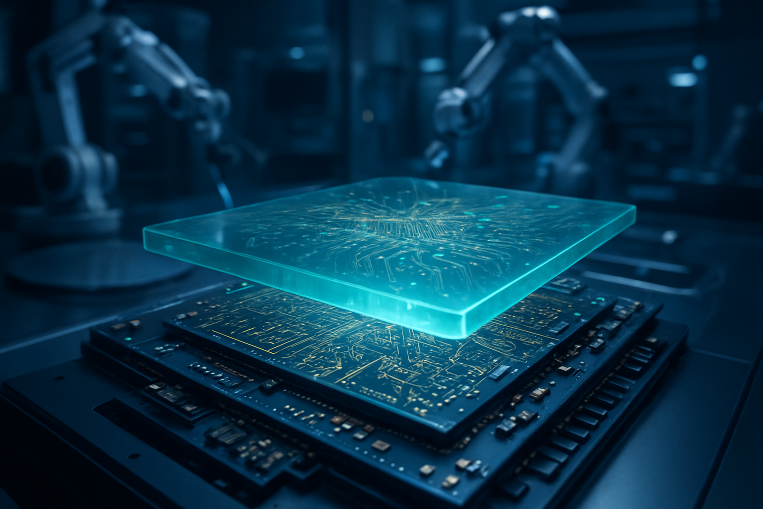
  • Chain Reaction Unleashes EL3CTRUM E31: A New Era of Efficiency in Bitcoin Mining Driven by Specialized Semiconductors

    Chain Reaction Unleashes EL3CTRUM E31: A New Era of Efficiency in Bitcoin Mining Driven by Specialized Semiconductors

    The cryptocurrency mining industry is buzzing with the recent announcement from Chain Reaction regarding its EL3CTRUM E31, a new suite of Bitcoin miners poised to redefine the benchmarks for energy efficiency and operational flexibility. This launch, centered around the groundbreaking EL3CTRUM A31 ASIC (Application-Specific Integrated Circuit), signifies a pivotal moment for large-scale mining operations, promising to significantly reduce operational costs and enhance profitability in an increasingly competitive landscape. With its cutting-edge 3nm process node technology, the EL3CTRUM E31 is not just an incremental upgrade but a generational leap, setting new standards for power efficiency and adaptability in the relentless pursuit of Bitcoin.

    The immediate significance of the EL3CTRUM E31 lies in its bold claim of delivering "sub-10 Joules per Terahash (J/TH)" efficiency, a metric that directly translates to lower electricity consumption per unit of computational power. This level of efficiency is critical as the global energy market remains volatile and environmental scrutiny on Bitcoin mining intensifies. Beyond raw power, the EL3CTRUM E31 emphasizes modularity, allowing miners to customize their infrastructure from the chip level up, and integrates advanced features like power curtailment and remote management. These innovations are designed to provide miners with unprecedented control and responsiveness to dynamic power markets, making the EL3CTRUM E31 a frontrunner in the race for sustainable and profitable Bitcoin production.

    Unpacking the Technical Marvel: The EL3CTRUM E31's Core Innovations

    At the heart of Chain Reaction's EL3CTRUM E31 system is the EL3CTRUM A31 ASIC, fabricated using an advanced 3nm process node. This miniaturization of transistor size is the primary driver behind its superior performance and energy efficiency. While samples are anticipated in May 2026 and volume shipments in Q3 2026, the projected specifications are already turning heads.

    The EL3CTRUM E31 is offered in various configurations to suit diverse operational needs and cooling infrastructures:

    • EL3CTRUM E31 Air: Offers a hash rate of 310 TH/s with 3472 W power consumption, achieving an efficiency of 11.2 J/TH.
    • EL3CTRUM E31 Hydro: Designed for liquid cooling, it boasts an impressive 880 TH/s hash rate at 8712 W, delivering a remarkable 9.9 J/TH efficiency.
    • EL3CTRUM E31 Immersion: Provides 396 TH/s at 4356 W, with an efficiency of 11.0 J/TH.

    The specialized ASICs are custom-designed for the SHA-256 algorithm used by Bitcoin, allowing them to perform this specific task with vastly greater efficiency than general-purpose CPUs or GPUs. Chain Reaction's commitment to pushing these boundaries is further evidenced by their active development of 2nm ASICs, promising even greater efficiencies in future iterations. This modular architecture, offering standalone A31 ASIC chips, H31 hashboards, and complete E31 units, empowers miners to optimize their systems for maximum scalability and a lower total cost of ownership. This flexibility stands in stark contrast to previous generations of more rigid, integrated mining units, allowing for tailored solutions based on regional power strategies, climate conditions, and existing facility infrastructure.

    Industry Ripples: Impact on Companies and Competitive Landscape

    The introduction of the EL3CTRUM E31 is set to create significant ripples across the Bitcoin mining industry, benefiting some while presenting formidable challenges to others. Chain Reaction, as the innovator behind this advanced technology, is positioned for substantial growth, leveraging its cutting-edge 3nm ASIC design and a robust supply chain.

    Several key players stand to benefit directly from this development. Core Scientific (NASDAQ: CORZ), a leading North American digital asset infrastructure provider, has a longstanding collaboration with Chain Reaction, recognizing ASIC innovation as crucial for differentiated infrastructure. This partnership allows Core Scientific to integrate EL3CTRUM technology to achieve superior efficiency and scalability. Similarly, ePIC Blockchain Technologies and BIT Mining Limited have also announced collaborations, aiming to deploy next-generation Bitcoin mining systems with industry-leading performance and low power consumption. For large-scale data center operators and industrial miners, the EL3CTRUM E31's efficiency and modularity offer a direct path to reduced operational costs and sustained profitability, especially in dynamic energy markets.

    Conversely, other ASIC manufacturers, such as industry stalwarts Bitmain and Whatsminer, will face intensified competitive pressure. The EL3CTRUM E31's "sub-10 J/TH" efficiency sets a new benchmark, compelling competitors to accelerate their research and development into smaller process nodes and more efficient architectures. Manufacturers relying on older process nodes or less efficient designs risk seeing their market share diminish if they cannot match Chain Reaction's performance metrics. This launch will likely hasten the obsolescence of current and older-generation mining hardware, forcing miners to upgrade more frequently to remain competitive. The emphasis on modular and customizable solutions could also drive a shift in the market, with large operators increasingly opting for components to integrate into custom data center designs, rather than just purchasing complete, off-the-shelf units.

    Wider Significance: Beyond the Mining Farm

    The advancements embodied by the EL3CTRUM E31 extend far beyond the immediate confines of Bitcoin mining, signaling broader trends within the technology and semiconductor industries. The relentless pursuit of efficiency and computational power in specialized hardware design mirrors the trajectory of AI, where purpose-built chips are essential for processing massive datasets and complex algorithms. While Bitcoin ASICs are distinct from AI chips, both fields benefit from the cutting-edge semiconductor manufacturing processes (e.g., 3nm, 2nm) that are pushing the limits of performance per watt.

    Intriguingly, there's a growing convergence between these sectors. Bitcoin mining companies, having established significant energy infrastructure, are increasingly exploring and even pivoting towards hosting AI and High-Performance Computing (HPC) operations. This synergy is driven by the shared need for substantial power and robust data center facilities. The expertise in managing large-scale digital infrastructure, initially developed for Bitcoin mining, is proving invaluable for the energy-intensive demands of AI, suggesting that advancements in Bitcoin mining hardware can indirectly contribute to the overall expansion of the AI sector.

    However, these advancements also bring wider concerns. While the EL3CTRUM E31's efficiency reduces energy consumption per unit of hash power, the overall energy consumption of the Bitcoin network remains a significant environmental consideration. As mining becomes more profitable, miners are incentivized to deploy more powerful hardware, increasing the total hash rate and, consequently, the network's total energy demand. The rapid technological obsolescence of mining hardware also contributes to a growing e-waste problem. Furthermore, the increasing specialization and cost of ASICs contribute to the centralization of Bitcoin mining, making it harder for individual miners to compete with large farms and potentially raising concerns about the network's decentralized ethos. The semiconductor industry, meanwhile, benefits from the demand but also faces challenges from the volatile crypto market and geopolitical tensions affecting supply chains. This evolution can be compared to historical tech milestones like the shift from general-purpose CPUs to specialized GPUs for graphics, highlighting a continuous trend towards optimized hardware for specific, demanding computational tasks.

    The Road Ahead: Future Developments and Expert Predictions

    The future of Bitcoin mining technology, particularly concerning specialized semiconductors, promises continued rapid evolution. In the near term (1-3 years), the industry will see a sustained push towards even smaller and more efficient ASIC chips. While 3nm ASICs like the EL3CTRUM A31 are just entering the market, the development of 2nm chips is already underway, with TSMC planning manufacturing by 2025 and Chain Reaction targeting a 2nm ASIC release in 2027. These advancements, leveraging innovative technologies like Gate-All-Around Field-Effect Transistors (GAAFETs), are expected to deliver further reductions in energy consumption and increases in processing speed. The entry of major players like Intel into the custom cryptocurrency product group also signals increased competition, which is likely to drive further innovation and potentially stabilize hardware pricing. Enhanced cooling solutions, such as hydro and immersion cooling, will also become increasingly standard to manage the heat generated by these powerful chips.

    Longer term (beyond 3 years), while the pursuit of miniaturization will continue, the fundamental economics of Bitcoin mining will undergo a significant shift. With the final Bitcoin projected to be mined around 2140, miners will eventually rely solely on transaction fees for revenue. This necessitates a robust fee market to incentivize miners and maintain network security. Furthermore, AI integration into mining operations is expected to deepen, optimizing power usage, hash rate performance, and overall operational efficiency. Beyond Bitcoin, the underlying technology of advanced ASICs holds potential for broader applications in High-Performance Computing (HPC) and encrypted AI computing, fields where Chain Reaction is already making strides with its "privacy-enhancing processors (3PU)."

    However, significant challenges remain. The ever-increasing network hash rate and difficulty, coupled with Bitcoin halving events (which reduce block rewards), will continue to exert immense pressure on miners to constantly upgrade equipment. High energy costs, environmental concerns, and semiconductor supply chain vulnerabilities exacerbated by geopolitical tensions will also demand innovative solutions and diversified strategies. Experts predict an unrelenting focus on efficiency, a continued geographic redistribution of mining power towards regions with abundant renewable energy and supportive policies, and intensified competition driving further innovation. Bullish forecasts for Bitcoin's price in the coming years suggest continued institutional adoption and market growth, which will sustain the incentive for these technological advancements.

    A Comprehensive Wrap-Up: Redefining the Mining Paradigm

    Chain Reaction's launch of the EL3CTRUM E31 marks a significant milestone in the evolution of Bitcoin mining technology. By leveraging advanced 3nm specialized semiconductors, the company is not merely offering a new product but redefining the paradigm for efficiency, modularity, and operational flexibility in the industry. The "sub-10 J/TH" efficiency target, coupled with customizable configurations and intelligent management features, promises substantial cost reductions and enhanced profitability for large-scale miners.

    This development underscores the critical role of specialized hardware in the cryptocurrency ecosystem and highlights the relentless pace of innovation driven by the demands of Proof-of-Work networks. It sets a new competitive bar for other ASIC manufacturers and will accelerate the obsolescence of less efficient hardware, pushing the entire industry towards more sustainable and technologically advanced solutions. While concerns around energy consumption, centralization, and e-waste persist, the EL3CTRUM E31 also demonstrates how advancements in mining hardware can intersect with and potentially benefit other high-demand computing fields like AI and HPC.

    Looking ahead, the industry will witness a continued "Moore's Law" effect in mining, with 2nm and even smaller chips on the horizon, alongside a growing emphasis on renewable energy integration and AI-driven operational optimization. The strategic partnerships forged by Chain Reaction with industry leaders like Core Scientific signal a collaborative approach to innovation that will be vital in navigating the challenges of increasing network difficulty and fluctuating market conditions. The EL3CTRUM E31 is more than just a miner; it's a testament to the ongoing technological arms race that defines the digital frontier, and its long-term impact will be keenly watched by tech journalists, industry analysts, and cryptocurrency enthusiasts alike in the weeks and months to come.

    This content is intended for informational purposes only and represents analysis of current AI developments.

    TokenRing AI delivers enterprise-grade solutions for multi-agent AI workflow orchestration, AI-powered development tools, and seamless remote collaboration platforms.
    For more information, visit https://www.tokenring.ai/.
  • Rambus Downgrade: A Valuation Reality Check Amidst the AI Semiconductor Boom

    Rambus Downgrade: A Valuation Reality Check Amidst the AI Semiconductor Boom

    On October 6, 2025, the semiconductor industry saw a significant development as financial firm Susquehanna downgraded Rambus (NASDAQ: RMBS) from "Positive" to "Neutral." This recalibration, while seemingly a step back, was primarily a valuation-driven decision, reflecting Susquehanna's view that Rambus's impressive 92% year-to-date stock surge had already priced in much of its anticipated upside. Despite the downgrade, Rambus shares experienced a modest 1.7% uptick in late morning trading, signaling a nuanced market reaction to a company deeply embedded in the burgeoning AI and data center landscape. This event serves as a crucial indicator of increasing investor scrutiny within a sector experiencing unprecedented growth, prompting a closer look at what this signifies for Rambus and the wider semiconductor market.

    The Nuance Behind the Numbers: A Deep Dive into Rambus's Valuation

    Susquehanna's decision to downgrade Rambus was not rooted in a fundamental skepticism of the company's technological prowess or market strategy. Instead, the firm concluded that Rambus's stock, trading at a P/E ratio of 48, had largely factored in a "best-case earnings scenario." The immediate significance for Rambus lies in this valuation adjustment, suggesting that while the company's prospects remain robust, particularly from server-driven product revenue (projected over 40% CAGR from 2025-2027) and IP revenue expansion, its current stock price reflects these positives, leading to a "Neutral" stance. Susquehanna also adjusted its price target for Rambus to $100 from $75, noting its proximity to the current share price and indicating a balanced risk/reward profile.

    Rambus stands as a critical player in the high-performance memory and interconnect space, offering technologies vital for modern AI and data center infrastructure. Its product portfolio includes cutting-edge DDR5 memory interface chips, such as Registering Clock Driver (RCD) Buffer Chips and Companion Chips, which are essential for AI servers and data centers, with Rambus commanding over 40% of the DDR5 RCD market. The transition to Gen3 DDR5 RCDs is expected to drive double-digit growth. Furthermore, Rambus is at the forefront of Compute Express Link (CXL) solutions, providing CXL 3.1 and PCIe 6.1 controllers with integrated Integrity and Data Encryption (IDE) modules, offering zero-latency security at high speeds. The company is also heavily invested in High-Bandwidth Memory (HBM) development, including HBM4 modules, crucial for next-generation AI workloads. Susquehanna’s analysis, while acknowledging these strong growth drivers, anticipated a modest decline in gross margins due to a shift towards faster-growing but lower-margin product revenue. Critically, the downgrade did not stem from concerns about Rambus's technological capabilities or the market adoption of CXL, but rather from the stock's already-rich valuation.

    Ripples in the Pond: Implications for AI Companies and the Semiconductor Ecosystem

    Given the valuation-driven nature of the downgrade, the immediate operational impact on other semiconductor companies, especially those focused on AI hardware and data center solutions, is likely to be limited. However, it could subtly influence investor perception and competitive dynamics within the industry.

    Direct competitors in the memory interface chip market, such as Montage Technology Co. Ltd. and Renesas Electronics Corporation, which collectively hold over 80% of the global market share, could theoretically see opportunities if Rambus's perceived momentum were to slow. In the broader IP licensing arena, major Electronic Design Automation (EDA) platforms like Cadence Design Systems (NASDAQ: CDNS) and Synopsys (NASDAQ: SNPS), both with extensive IP portfolios, might attract increased customer interest. Memory giants such as Micron Technology (NASDAQ: MU), SK Hynix, and Samsung (KRX: 005930), deeply involved in advanced memory technologies like HBM and LPCAMM2, could also benefit from any perceived shift in the competitive landscape.

    Major AI hardware developers and data center solution providers, including NVIDIA (NASDAQ: NVDA), Intel (NASDAQ: INTC), AMD (NASDAQ: AMD), and hyperscalers like Amazon Web Services (NASDAQ: AMZN), Google Cloud (NASDAQ: GOOG), and Microsoft Azure (NASDAQ: MSFT), are unlikely to face immediate disruptions. Rambus maintains strong partnerships, evidenced by Intel integrating Rambus chipsets into Core Ultra processors and NVIDIA renewing patent licenses. Disruptions would only become a concern if the downgrade signaled underlying operational or financial instability, leading to supply chain issues, delayed innovation in next-generation memory interfaces, or uncertainty in IP licensing. Currently, there is no indication that such severe disruptions are imminent. Rambus’s competitors, particularly the larger, more diversified players, often leverage their comprehensive product offerings, established market share, and robust R&D pipelines as strategic advantages, which they may subtly emphasize in the wake of such valuation adjustments.

    Beyond Rambus: The Broader Significance for the AI Semiconductor Landscape

    The valuation-driven downgrade of Rambus, while specific to the company, resonates within broader semiconductor market trends, especially concerning the relentless growth of AI and data centers. It underscores a growing cautious sentiment among investors, even towards companies integral to the AI revolution. While the AI boom is real and driving unprecedented demand, the market is becoming increasingly discerning about current valuations. High stock gains, even when justified by underlying technological importance, can lead to a perception of being "fully priced," making these companies vulnerable to corrections if future earnings do not meet aggressive forecasts.

    For specialized semiconductor companies, this implies that strong technological positioning in AI is necessary but not sufficient to sustain perpetual stock growth without corresponding, outperforming financial results. The semiconductor industry, particularly its AI-related segments, is facing increasing concerns about overvaluation and the potential for market corrections. The collective market capitalization of leading tech giants, including AI chipmakers, has reached historic highs, prompting questions about whether earnings growth can justify current stock prices. While AI spending will continue, the pace of growth might decelerate below investor expectations, leading to sharp declines. Furthermore, the industry remains inherently cyclical and sensitive to economic fluctuations, with geopolitical factors like stringent export controls profoundly reshaping global supply chains, adding new layers of complexity and risk.

    This environment shares some characteristics with previous periods of investor recalibration, such as the 1980s DRAM crash or the dot-com bubble. However, key differences exist today, including an improved memory oligopoly, a shift in primary demand drivers from consumer electronics to AI data centers, and the unprecedented "weaponization" of supply chains through geopolitical competition.

    The Road Ahead: Navigating Future Developments and Challenges

    The future for Rambus and the broader semiconductor market, particularly concerning AI and data center technologies, points to continued, substantial growth, albeit with inherent challenges. Rambus is well-positioned for near-term growth, with expectations of increased production for DDR5 PMICs through 2025 and beyond, and significant growth anticipated in companion chip revenue in 2026 with the launch of MRDIMM technology. The company's ongoing R&D in DDR6 and HBM aims to maintain its technical leadership.

    Rambus’s technologies are critical enablers for next-generation AI and data center infrastructure. DDR5 memory is essential for data-intensive AI applications, offering higher data transfer rates and improved power efficiency. CXL is set to revolutionize data center architectures by enabling memory pooling and disaggregated systems, crucial for memory-intensive AI/ML workloads. HBM remains indispensable for training and inferencing complex AI models due to its unparalleled speed and efficiency, with HBM4 anticipated to deliver substantial leaps in bandwidth. Furthermore, Rambus’s CryptoManager Security IP solutions provide multi-tiered, quantum-safe protection, vital for safeguarding data centers against evolving cyberthreats.

    However, challenges persist. HBM faces high production costs, complex manufacturing, and a severe supply chain crunch, leading to undersupply. For DDR5, the high cost of transitioning from DDR4 and potential semiconductor shortages could hinder adoption. CXL, while promising, is still a nascent market requiring extensive testing, software optimization, and ecosystem alignment. The broader semiconductor market also contends with geopolitical tensions, tariffs, and potential over-inventory builds. Experts, however, remain largely bullish on both Rambus and the semiconductor market, emphasizing AI-driven memory innovation and IP growth. Baird, for instance, initiated coverage of Rambus with an Outperform rating, highlighting its central role in AI-driven performance increases and "first-to-market solutions addressing performance bottlenecks."

    A Measured Outlook: Key Takeaways and What to Watch For

    The Susquehanna downgrade of Rambus serves as a timely reminder that even amidst the exhilarating ascent of the AI semiconductor market, fundamental valuation principles remain paramount. It's not a commentary on Rambus's inherent strength or its pivotal role in enabling AI advancements, but rather a recalibration of investor expectations following a period of exceptional stock performance. Rambus continues to be a critical "memory architect" for AI and high-performance computing, with its DDR5, CXL, HBM, and security IP solutions forming the backbone of next-generation data centers.

    This development, while not a landmark event in AI history, is significant in reflecting the maturing market dynamics and intense investor scrutiny. It underscores that sustained stock growth requires not just technological leadership, but also a clear pathway to profitable growth that justifies market valuations. In the long term, such valuation-driven recalibrations will likely foster increased investor scrutiny, a greater focus on fundamentals, and encourage industry players to prioritize profitable growth, diversification, and strategic partnerships.

    In the coming weeks and months, investors and industry observers should closely monitor Rambus’s Q3 2025 earnings and future guidance for insights into its actual financial performance against expectations. Key indicators to watch include the adoption rates of DDR5 and HBM4 in AI infrastructure, progress in CXL and security IP solutions, and the evolving competitive landscape in AI memory. The overall health of the semiconductor market, global AI investment trends, and geopolitical developments will also play crucial roles in shaping the future trajectory of Rambus and its peers. While the journey of AI innovation is far from over, the market is clearly entering a phase where tangible results and sustainable growth will be rewarded with increasing discernment.


    This content is intended for informational purposes only and represents analysis of current AI developments.

    TokenRing AI delivers enterprise-grade solutions for multi-agent AI workflow orchestration, AI-powered development tools, and seamless remote collaboration platforms.
    For more information, visit https://www.tokenring.ai/.

  • ESD Industry Soars to $5.1 Billion in Q2 2025, Fueling AI’s Hardware Revolution

    ESD Industry Soars to $5.1 Billion in Q2 2025, Fueling AI’s Hardware Revolution

    San Francisco, CA – October 6, 2025 – The Electronic System Design (ESD) industry has reported a robust and pivotal performance in the second quarter of 2025, achieving an impressive $5.1 billion in revenue. This significant figure represents an 8.6% increase compared to Q2 2024, signaling a period of sustained and accelerated growth for the foundational sector that underpins the entire semiconductor ecosystem. As the demand for increasingly complex and specialized chips for Artificial Intelligence (AI), 5G, and IoT applications intensifies, the ESD industry’s expansion is proving critical, directly fueling the innovation and advancement of semiconductor design tools and, by extension, the future of AI hardware.

    This strong financial showing, which saw the industry's four-quarter moving average revenue climb by 10.4%, underscores the indispensable role of Electronic Design Automation (EDA) tools in navigating the intricate challenges of modern chip development. The consistent upward trajectory in revenue reflects the global electronics industry's reliance on sophisticated software to design, verify, and manufacture the advanced integrated circuits (ICs) that power everything from data centers to autonomous vehicles. This growth is particularly significant as the industry moves beyond traditional scaling limits, with AI-powered EDA becoming the linchpin for continued innovation in semiconductor performance and efficiency.

    AI and Digital Twins Drive a New Era of Chip Design

    The core of the ESD industry's recent surge lies in the transformative integration of Artificial Intelligence (AI), Machine Learning (ML), and digital twin technologies into Electronic Design Automation (EDA) tools. This paradigm shift marks a fundamental departure from traditional, often manual, chip design methodologies, ushering in an era of unprecedented automation, optimization, and predictive capabilities across the entire design stack. Companies are no longer just automating tasks; they are empowering AI to actively participate in the design process itself.

    AI-driven tools are revolutionizing critical stages of chip development. In automated layout and floorplanning, reinforcement learning algorithms can evaluate millions of potential floorplans, identifying superior configurations that far surpass human-derived designs. For logic optimization and synthesis, ML models analyze Hardware Description Language (HDL) code to suggest improvements, leading to significant reductions in power consumption and boosts in performance. Furthermore, AI assists in rapid design space exploration, quickly identifying optimal microarchitectural configurations for complex systems-on-chips (SoCs). This enables significant improvements in power, performance, and area (PPA) optimization, with some AI-driven tools demonstrating up to a 40% reduction in power consumption and a three to five times increase in design productivity.

    The impact extends powerfully into verification and debugging, historically a major bottleneck in chip development. AI-driven verification automates test case generation, proactively detects design flaws, and predicts failure points before manufacturing, drastically reducing verification effort and improving bug detection rates. Digital twin technology, integrating continuously updated virtual representations of physical systems, allows designers to rigorously test chips against highly accurate simulations of entire subsystems and environments. This "shift left" in the design process enables earlier and more comprehensive validation, moving beyond static models to dynamic, self-learning systems that evolve with real-time data, ultimately leading to faster development cycles (months into weeks) and superior product quality.

    Competitive Landscape Reshaped: EDA Giants and Tech Titans Leverage AI

    The robust growth of the ESD industry, propelled by AI-powered EDA, is profoundly reshaping the competitive landscape for major AI companies, tech giants, and semiconductor startups alike. At the forefront are the leading EDA tool vendors, whose strategic integration of AI into their offerings is solidifying their market dominance and driving innovation.

    Synopsys, Inc. (NASDAQ: SNPS), a pioneer in full-stack AI-driven EDA, has cemented its leadership with its Synopsys.ai suite. This comprehensive platform, including DSO.ai for PPA optimization, VSO.ai for verification, and TSO.ai for test coverage, promises over three times productivity increases and up to 20% better quality of results. Synopsys is also expanding its generative AI (GenAI) capabilities with Synopsys.ai Copilot and developing AgentEngineer technology for autonomous decision-making in chip design. Similarly, Cadence Design Systems, Inc. (NASDAQ: CDNS) has adopted an "AI-first approach," with solutions like Cadence Cerebrus Intelligent Chip Explorer optimizing multiple blocks simultaneously, showing up to 20% improvements in PPA and 60% performance boosts on specific blocks. Cadence's vision of "Level 5 Autonomy" aims for AI to handle end-to-end chip design, accelerating cycles by as much as a month, with its AI-assisted platforms already used by over 1,000 customers. Siemens EDA, a division of Siemens AG (ETR: SIE), is also aggressively embedding AI into its core tools, with its EDA AI System offering secure, advanced generative and agentic AI capabilities. Its solutions, like Aprisa AI software, deliver significant productivity increases (10x), faster time to tapeout (3x), and better PPA (10%).

    Beyond the EDA specialists, major tech giants like Alphabet Inc. (NASDAQ: GOOGL), Amazon.com, Inc. (NASDAQ: AMZN), Microsoft Corporation (NASDAQ: MSFT), and Meta Platforms, Inc. (NASDAQ: META) are increasingly becoming their own chip architects. Leveraging AI-powered EDA, they design custom silicon, such as Google's Tensor Processing Units (TPUs), optimized for their proprietary AI workloads. This strategy enhances cloud services, reduces reliance on external vendors, and provides significant strategic advantages in cost efficiency and performance. For specialized AI hardware developers like NVIDIA Corporation (NASDAQ: NVDA) and Advanced Micro Devices, Inc. (NASDAQ: AMD), AI-powered EDA tools are indispensable for designing high-performance GPUs and AI-specific processors. Furthermore, the "democratization of design" facilitated by cloud-based, AI-amplified EDA solutions is lowering barriers to entry for semiconductor startups, enabling them to develop customized chips more efficiently and cost-effectively for emerging niche applications in edge computing and IoT.

    The Broader Significance: Fueling the AI Revolution and Extending Moore's Law

    The ESD industry's robust growth, driven by AI-powered EDA, represents a pivotal development within the broader AI landscape. It signifies a "virtuous cycle" where advanced AI-powered tools design better AI chips, which, in turn, accelerate further AI development. This symbiotic relationship is crucial as current AI trends, including the proliferation of generative AI, large language models (LLMs), and agentic AI, demand increasingly powerful and energy-efficient hardware. The AI hardware market is diversifying rapidly, moving from general-purpose computing to domain-specific architectures meticulously crafted for AI workloads, a trend directly supported by the capabilities of modern EDA.

    The societal and economic impacts are profound. AI-driven EDA tools significantly compress development timelines, enabling faster introduction of new technologies across diverse sectors, from smart homes and autonomous vehicles to advanced robotics and drug discovery. The AI chip market is projected to exceed $100 billion by 2030, with AI itself expected to contribute over $15.7 trillion to global GDP through enhanced productivity and new market creation. While AI automates repetitive tasks, it also transforms the job market, freeing engineers to focus on architectural innovation and high-level problem-solving, though it necessitates a workforce with new skills in AI and data science. Critically, AI-powered EDA is instrumental in extending the relevance of Moore's Law, pushing the boundaries of chip capabilities even as traditional transistor scaling faces physical and economic limits.

    However, this revolution is not without its concerns. The escalating complexity of chips, now containing billions or even trillions of transistors, poses new challenges for verification and validation of AI-generated designs. High implementation costs, the need for vast amounts of high-quality data, and ethical considerations surrounding AI explainability and potential biases in algorithms are significant hurdles. The surging demand for skilled engineers who understand both AI and semiconductor design is creating a global talent gap, while the immense computational resources required for training sophisticated AI models raise environmental sustainability concerns. Despite these challenges, the current era, often dubbed "EDA 4.0," marks a distinct evolutionary leap, moving beyond mere automation to generative and agentic AI that actively designs, optimizes, and even suggests novel solutions, fundamentally reshaping the future of technology.

    The Horizon: Autonomous Design and Pervasive AI

    Looking ahead, the ESD industry and AI-powered EDA tools are poised for even more transformative developments, promising a future of increasingly autonomous and intelligent chip design. In the near term, AI will continue to enhance existing workflows, automating tasks like layout generation and verification, and acting as an intelligent assistant for scripting and collateral generation. Cloud-based EDA solutions will further democratize access to high-performance computing for design and verification, fostering greater collaboration and enabling real-time design rule checking to catch errors earlier.

    The long-term vision points towards truly autonomous design flows and "AI-native" methodologies, where self-learning systems generate and optimize circuits with minimal human oversight. This will be critical for the shift towards multi-die assemblies and 3D-ICs, where AI will be indispensable for optimizing complex chiplet-based architectures, thermal management, and signal integrity. AI is expected to become pervasive, impacting every aspect of chip design, from initial specification to tape-out and beyond, blurring the lines between human creativity and machine intelligence. Experts predict that design cycles that once took months or years could shrink to weeks, driven by real-time analytics and AI-guided decisions. The industry is also moving towards autonomous semiconductor manufacturing, where AI, IoT, and digital twins will detect and resolve process issues with minimal human intervention.

    However, challenges remain. Effective data management, bridging the expertise gap between AI and semiconductor design, and building trust in "black box" AI algorithms through rigorous validation are paramount. Ethical considerations regarding job impact and potential "hallucinations" from generative AI systems also need careful navigation. Despite these hurdles, the consensus among experts is that AI will lead to an evolution rather than a complete disruption of EDA, making engineers more productive and helping to bridge the talent gap. The demand for more efficient AI accelerators will continue to drive innovation, with companies racing to create new architectures, including neuromorphic chips, optimized for specific AI workloads.

    A New Era for AI Hardware: The Road Ahead

    The Electronic System Design industry's impressive $5.1 billion revenue in Q2 2025 is far more than a financial milestone; it is a clear indicator of a profound paradigm shift in how electronic systems are conceived, designed, and manufactured. This robust growth, overwhelmingly driven by the integration of AI, machine learning, and digital twin technologies into EDA tools, underscores the industry's critical role as the bedrock for the ongoing AI revolution. The ability to design increasingly complex, high-performance, and energy-efficient chips with unprecedented speed and accuracy is directly enabling the next generation of AI advancements, from sophisticated generative models to pervasive intelligent edge devices.

    This development marks a significant chapter in AI history, moving beyond software-centric breakthroughs to a fundamental transformation of the underlying hardware infrastructure. The synergy between AI and EDA is not merely an incremental improvement but a foundational re-architecture of the design process, allowing for the extension of Moore's Law and the creation of entirely new categories of specialized AI hardware. The competitive race among EDA giants, tech titans, and nimble startups to harness AI for chip design will continue to accelerate, leading to faster innovation cycles and more powerful computing capabilities across all sectors.

    In the coming weeks and months, the industry will be watching for continued advancements in AI-driven design automation, particularly in areas like multi-die system optimization and autonomous design flows. The development of a workforce skilled in both AI and semiconductor engineering will be crucial, as will addressing the ethical and environmental implications of this rapidly evolving technology. As the ESD industry continues its trajectory of growth, it will remain a vital barometer for the health and future direction of both the semiconductor industry and the broader AI landscape, acting as the silent architect of our increasingly intelligent world.

    TokenRing AI delivers enterprise-grade solutions for multi-agent AI workflow orchestration, AI-powered development tools, and seamless remote collaboration platforms. For more information, visit https://www.tokenring.ai/.