In the early weeks of 2026, the artificial intelligence industry has reached a pivotal realization: the race for dominance is no longer being won solely by those with the smallest transistors, but by those who can best "stitch" them together. At the heart of this paradigm shift is Taiwan Semiconductor Manufacturing Company (TSMC) (NYSE: TSM) and its proprietary CoWoS (Chip-on-Wafer-on-Substrate) technology. Once a niche back-end process, CoWoS has emerged as the single most critical bridge in the global AI supply chain, dictating the production timelines of every major AI accelerator from the NVIDIA (NASDAQ: NVDA) Blackwell series to the newly announced Rubin architecture.
The significance of this technology cannot be overstated. As the industry grapples with the physical limits of traditional silicon scaling, CoWoS has become the essential medium for integrating logic chips with High Bandwidth Memory (HBM). Without it, the massive Large Language Models (LLMs) that define 2026—now exceeding 100 trillion parameters—would be physically impossible to run. As TSMC’s advanced packaging capacity hits record highs this month, the bottleneck that once paralyzed the AI market in 2024 is finally beginning to ease, signaling a new era of high-volume, hyper-integrated compute.
The Architecture of Integration: Unpacking the CoWoS Family
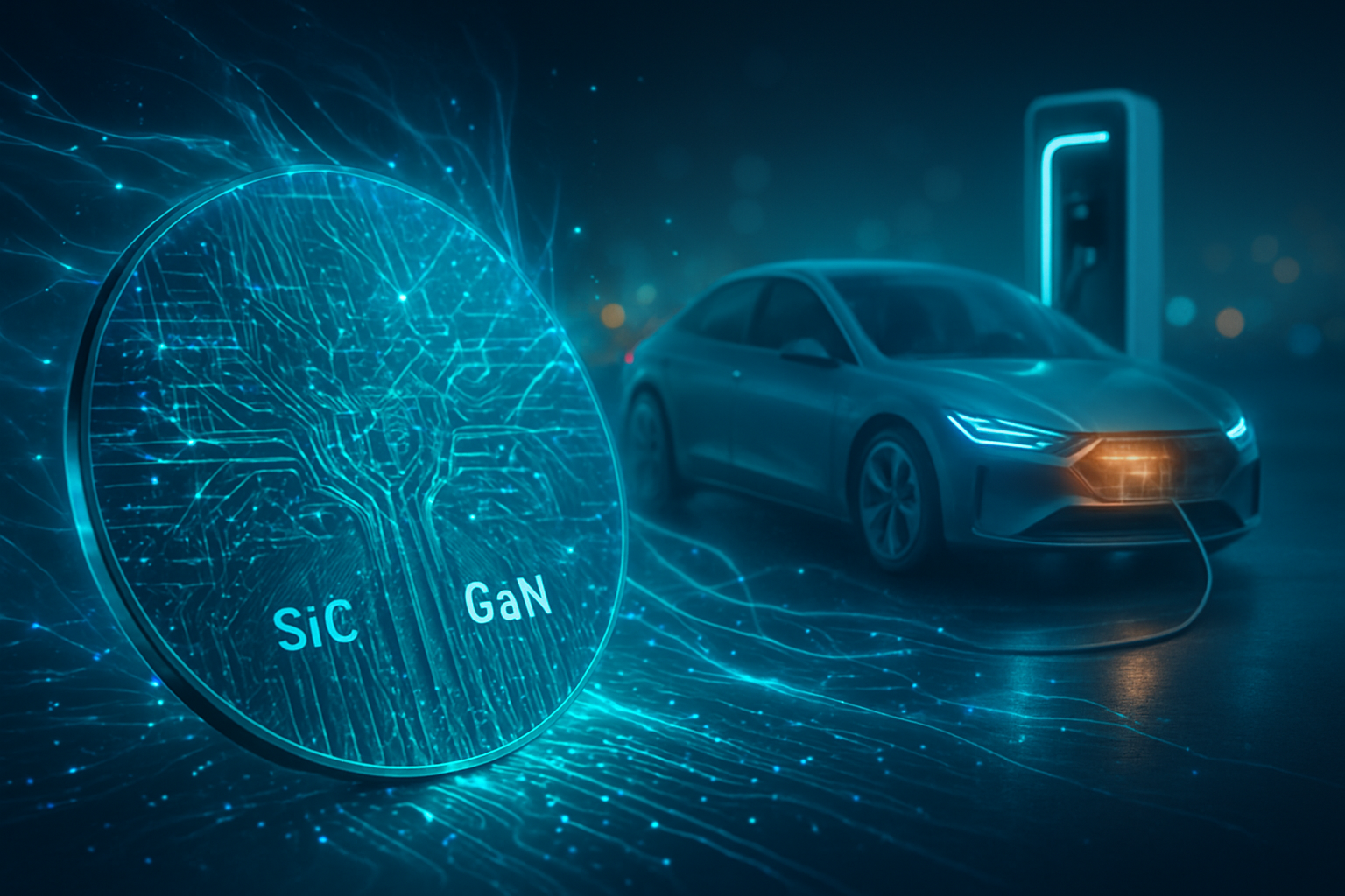
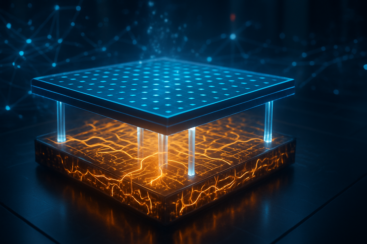
Technically, CoWoS is a 2.5D packaging technology that allows multiple silicon dies to be placed side-by-side on a silicon interposer, which then sits on a larger substrate. This arrangement allows for an unprecedented number of interconnections between the GPU and its memory, drastically reducing latency and increasing bandwidth. By early 2026, TSMC has evolved this platform into three distinct variants: CoWoS-S (Silicon), CoWoS-R (RDL), and the industry-dominant CoWoS-L (Local Interconnect). CoWoS-L has become the gold standard for high-end AI chips, using small silicon bridges to connect massive compute dies, allowing for packages that are up to nine times larger than a standard lithography "reticle" limit.
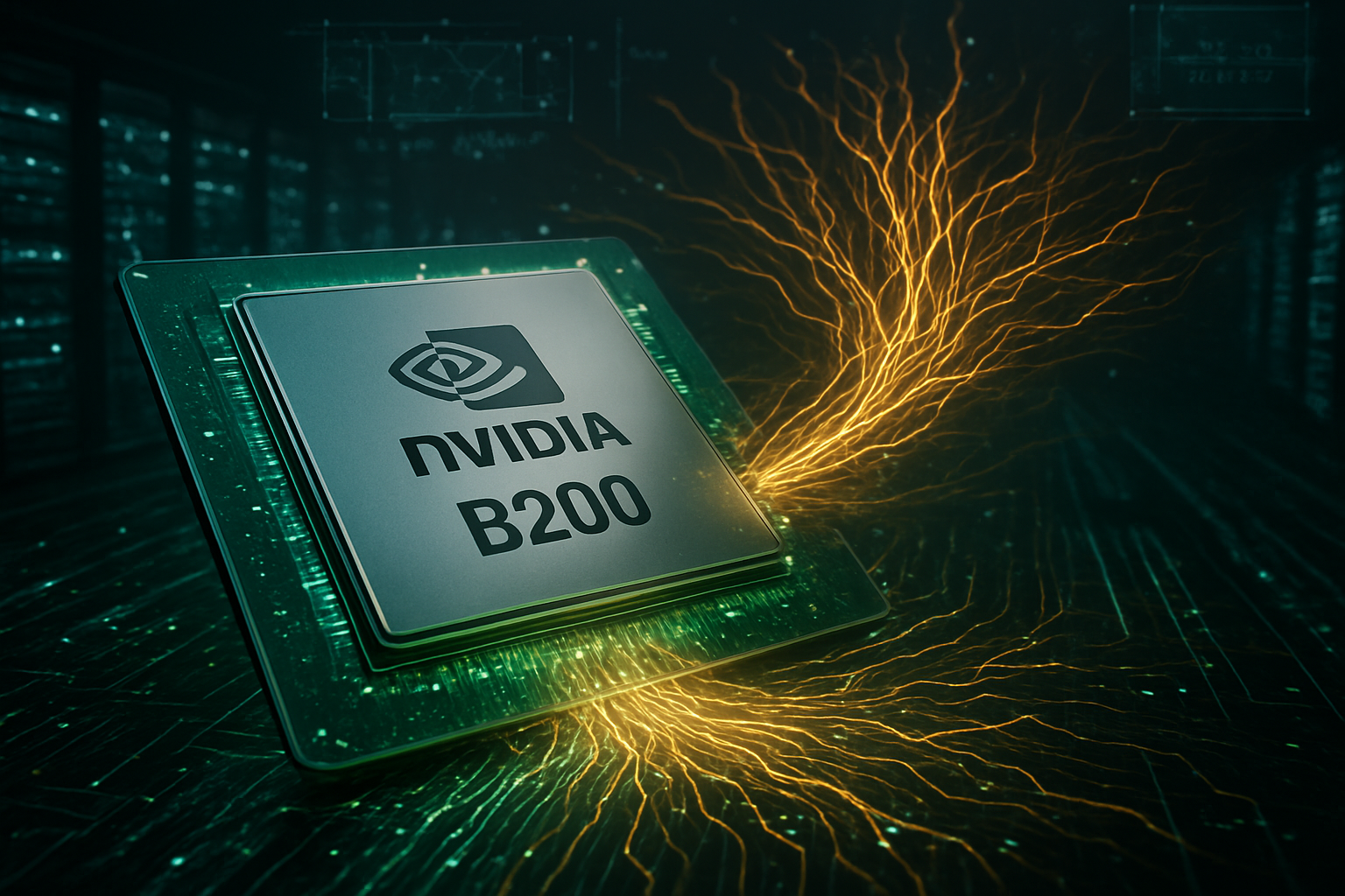
The shift to CoWoS-L was the technical catalyst for NVIDIA’s B200 and the transition to the R100 (Rubin) GPUs showcased at CES 2026. These chips require the integration of up to 12 or 16 HBM4 (High Bandwidth Memory 4) stacks, which utilize a 2048-bit interface—double that of the previous generation. This leap in complexity means that standard "flip-chip" packaging, which uses much larger connection bumps, is no longer viable. Experts in the research community have noted that we are witnessing the transition from "back-end assembly" to "system-level architecture," where the package itself acts as a massive, high-speed circuit board.
This advancement differs from existing technology primarily in its density and scale. While Intel (NASDAQ: INTC) uses its EMIB (Embedded Multi-die Interconnect Bridge) and Foveros stacking, TSMC has maintained a yield advantage by perfecting its "Local Silicon Interconnect" (LSI) bridges. These bridges allow TSMC to stitch together two "reticle-sized" dies into one monolithic processor, effectively circumventing the laws of physics that limit how large a single chip can be printed. Industry analysts from Yole Group have described this as the "Post-Moore Era," where performance gains are driven by how many components you can fit into a single 10cm x 10cm package.
Market Dominance and the "Foundry 2.0" Strategy
The strategic implications of CoWoS dominance have fundamentally reshaped the semiconductor market. TSMC is no longer just a foundry that prints wafers; it has evolved into a "System Foundry" under a model known as Foundry 2.0. By bundling wafer fabrication with advanced packaging and testing, TSMC has created a "strategic lock-in" for the world's most valuable tech companies. NVIDIA (NASDAQ: NVDA) has reportedly secured nearly 60% of TSMC's total 2026 CoWoS capacity, which is projected to reach 130,000 wafers per month by year-end. This massive allocation gives NVIDIA a nearly insurmountable lead in supply-chain reliability over smaller rivals.
Other major players are scrambling to secure their slice of the interposer. Broadcom (NASDAQ: AVGO), the primary architect of custom AI ASICs for Google and Meta, holds approximately 15% of the capacity, while Advanced Micro Devices (NASDAQ: AMD) has reserved 11% for its Instinct MI350 and MI400 series. For these companies, CoWoS allocation is more valuable than cash; it is the "permission to grow." Companies like Marvell (NASDAQ: MRVL) have also benefited, utilizing CoWoS-R for cost-effective networking chips that power the backbone of the global data center expansion.
This concentration of power has forced competitors like Samsung (KRX: 005930) to offer "turnkey" alternatives. Samsung’s I-Cube and X-Cube technologies are being marketed to customers who were "squeezed out" of TSMC’s schedule. Samsung’s unique advantage is its ability to manufacture the logic, the HBM4, and the packaging all under one roof—a vertical integration that TSMC, which does not make memory, cannot match. However, the industry’s deep familiarity with TSMC’s CoWoS design rules has made migration difficult, reinforcing TSMC's position as the primary gatekeeper of AI hardware.
Geopolitics and the Quest for "Silicon Sovereignty"
The wider significance of CoWoS extends beyond the balance sheets of tech giants and into the realm of national security. Because nearly all high-end CoWoS packaging is performed in Taiwan—specifically at TSMC’s massive new AP7 and AP8 plants—the global AI economy remains tethered to a single geographic point of failure. This has given rise to the concept of "AI Chip Sovereignty," where nations view the ability to package chips as a vital national interest. The 2026 "Silicon Pact" between the U.S. and its allies has accelerated efforts to reshore this capability, leading to the landmark partnership between TSMC and Amkor (NASDAQ: AMKR) in Peoria, Arizona.
This Arizona facility represents the first time a complete, end-to-end advanced packaging supply chain for AI chips has existed on U.S. soil. While it currently only handles a fraction of the volume seen in Taiwan, its presence provides a "safety valve" for lead customers like Apple and NVIDIA. Concerns remain, however, regarding the "Silicon Shield"—the theory that Taiwan’s indispensability to the AI world prevents military conflict. As advanced packaging capacity becomes more distributed globally, some geopolitical analysts worry that the strategic deterrent provided by TSMC's Taiwan-based gigafabs may eventually weaken.
Comparatively, the packaging bottleneck of 2024–2025 is being viewed by historians as the modern equivalent of the 1970s oil crisis. Just as oil powered the industrial age, "Advanced Packaging Interconnects" power the intelligence age. The transition from circular 300mm wafers to rectangular "Panel-Level Packaging" (PLP) is the next milestone, intended to increase the usable surface area for chips by over 300%. This shift is essential for the "Super-chips" of 2027, which are expected to integrate trillions of transistors and consume kilowatts of power, pushing the limits of current cooling and delivery systems.
The Horizon: From 2.5D to 3D and Glass Substrates
Looking forward, the industry is already moving toward "3D Silicon" architectures that will make current CoWoS technology look like a precursor. Expected in late 2026 and throughout 2027 is the mass adoption of SoIC (System on Integrated Chips), which allows for true 3D stacking of logic-on-logic without the use of micro-bumps. This "bumpless bonding" allows chips to be stacked vertically with interconnect densities that are orders of magnitude higher than CoWoS. When combined with CoWoS (a configuration often called 3.5D), it allows for a "skyscraper" of processors that the software interacts with as a single, massive monolithic chip.
Another revolutionary development on the horizon is the shift to Glass Substrates. Leading companies, including Intel and Samsung, are piloting glass as a replacement for organic resins. Glass provides better thermal stability and allows for even tighter interconnect pitches. Intel’s Chandler facility is predicted to begin high-volume manufacturing of glass-based AI packages by the end of this year. Additionally, the integration of Co-Packaged Optics (CPO)—using light instead of electricity to move data—is expected to solve the burgeoning power crisis in data centers by 2028.
However, these future applications face significant challenges. The thermal management of 3D-stacked chips is a major hurdle; as chips get denser, getting the heat out of the center of the "skyscraper" becomes a feat of extreme engineering. Furthermore, the capital expenditure required to build these next-generation packaging plants is staggering, with a single Panel-Level Packaging line costing upwards of $2 billion. Experts predict that only a handful of "Super-Foundries" will survive this capital-intensive transition, leading to further consolidation in the semiconductor industry.
Conclusion: A New Chapter in AI History
The importance of TSMC’s CoWoS technology in 2026 marks a definitive chapter in the history of computing. We have moved past the era where a chip was defined by its transistors alone. Today, a chip is defined by its connections. TSMC’s foresight in investing in advanced packaging a decade ago has allowed it to become the indispensable architect of the AI revolution, holding the keys to the world's most powerful compute engines.
As we look at the coming weeks and months, the primary indicators to watch will be the "yield ramp" of HBM4 integration and the first production runs of Panel-Level Packaging. These developments will determine if the AI industry can maintain its current pace of exponential growth or if it will hit another physical wall. For now, the "Silicon Squeeze" has eased, but the hunger for more integrated, more powerful, and more efficient chips remains insatiable. The world is no longer just building chips; it is building "Systems-in-Package," and TSMC’s CoWoS is the thread that holds that future together.
This content is intended for informational purposes only and represents analysis of current AI developments.
TokenRing AI delivers enterprise-grade solutions for multi-agent AI workflow orchestration, AI-powered development tools, and seamless remote collaboration platforms.
For more information, visit https://www.tokenring.ai/.
Generated on January 19, 2026.