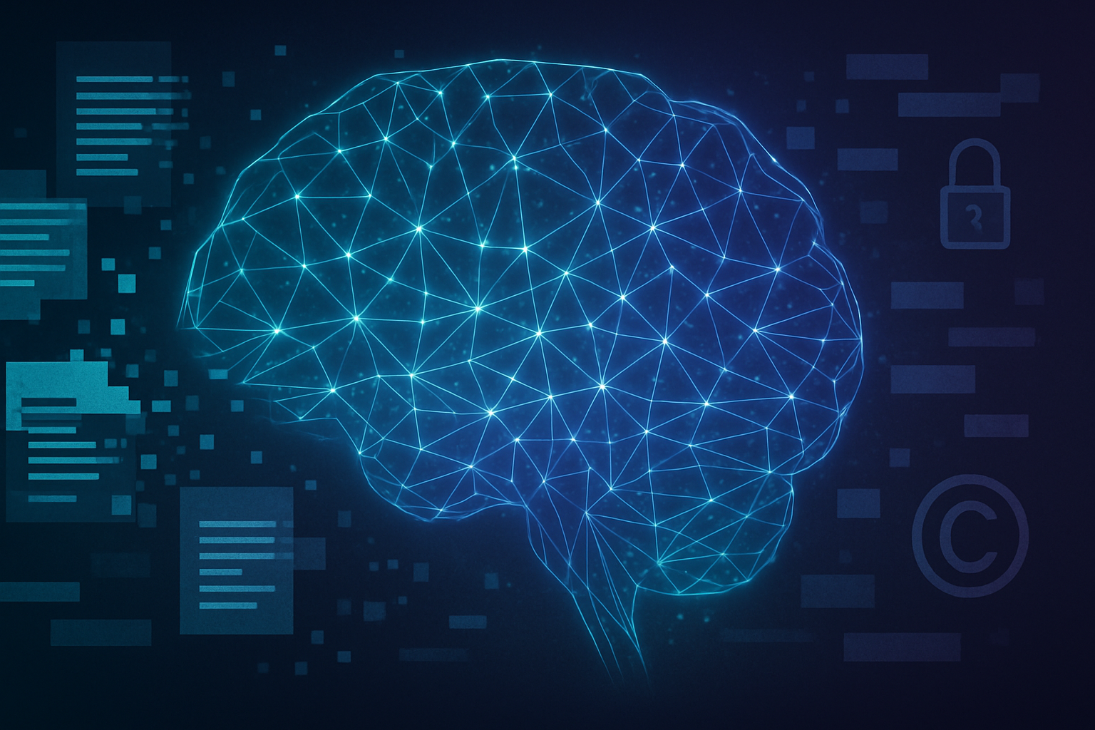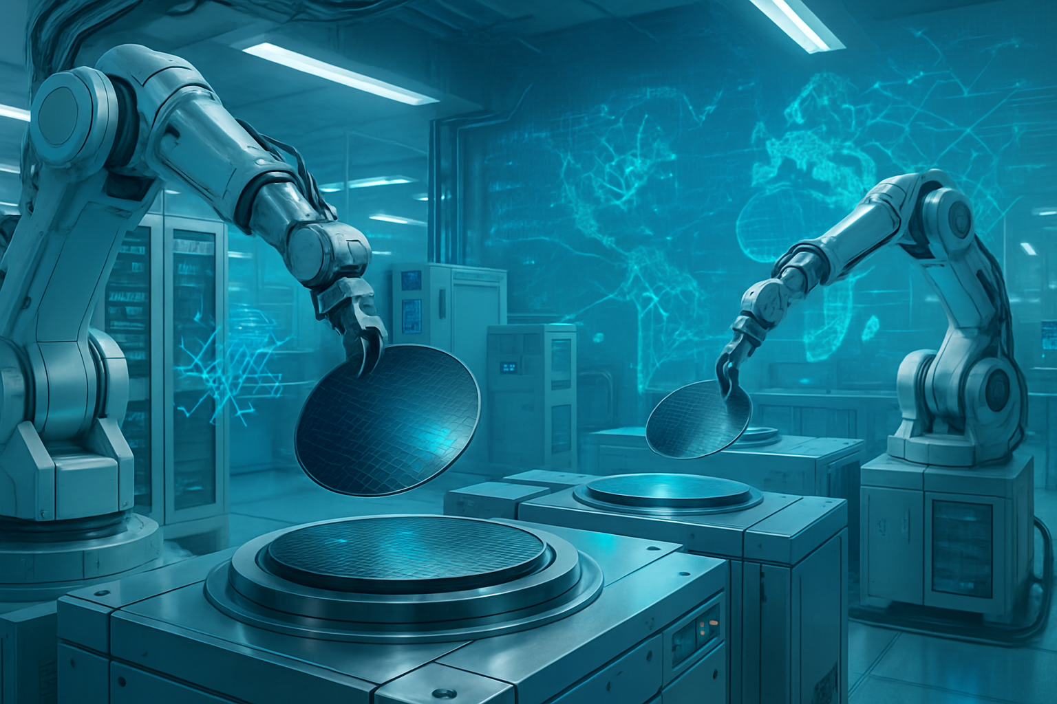
In a landmark move poised to redefine the application of artificial intelligence, CoreWeave, a specialized provider of high-performance cloud infrastructure, announced its agreement to acquire Monolith AI. The acquisition, unveiled around October 6, 2025, marks a pivotal moment, signaling CoreWeave's aggressive expansion beyond traditional AI workloads into the intricate world of industrial design and complex engineering challenges. This strategic integration is set to create a formidable, full-stack AI platform, democratizing advanced AI capabilities for sectors previously constrained by the sheer complexity and cost of R&D.
This strategic acquisition by CoreWeave aims to bridge the gap between cutting-edge AI infrastructure and the demanding requirements of industrial and manufacturing enterprises. By bringing Monolith AI's specialized machine learning capabilities under its wing, CoreWeave is not just growing its cloud services; it's cultivating an ecosystem where AI can directly influence and optimize the design, testing, and development of physical products. This represents a significant shift, moving AI from primarily software-centric applications to tangible, real-world engineering solutions.
The Fusion of High-Performance Cloud and Physics-Informed Machine Learning
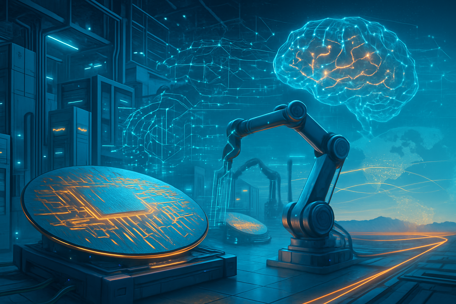
Monolith AI stands out as a pioneer in applying artificial intelligence to solve some of the most intractable problems in physics and engineering. Its core technology leverages machine learning models trained on vast datasets of historical simulation and testing data to predict outcomes, identify anomalies, and recommend optimal next steps in the design process. This allows engineers to make faster, more reliable decisions without requiring deep machine learning expertise or extensive coding. The cloud-based platform, with its intuitive user interface, is already in use by major engineering firms like Nissan (TYO: 7201), BMW (FWB: BMW), and Honeywell (NASDAQ: HON), enabling them to dramatically reduce product development cycles.
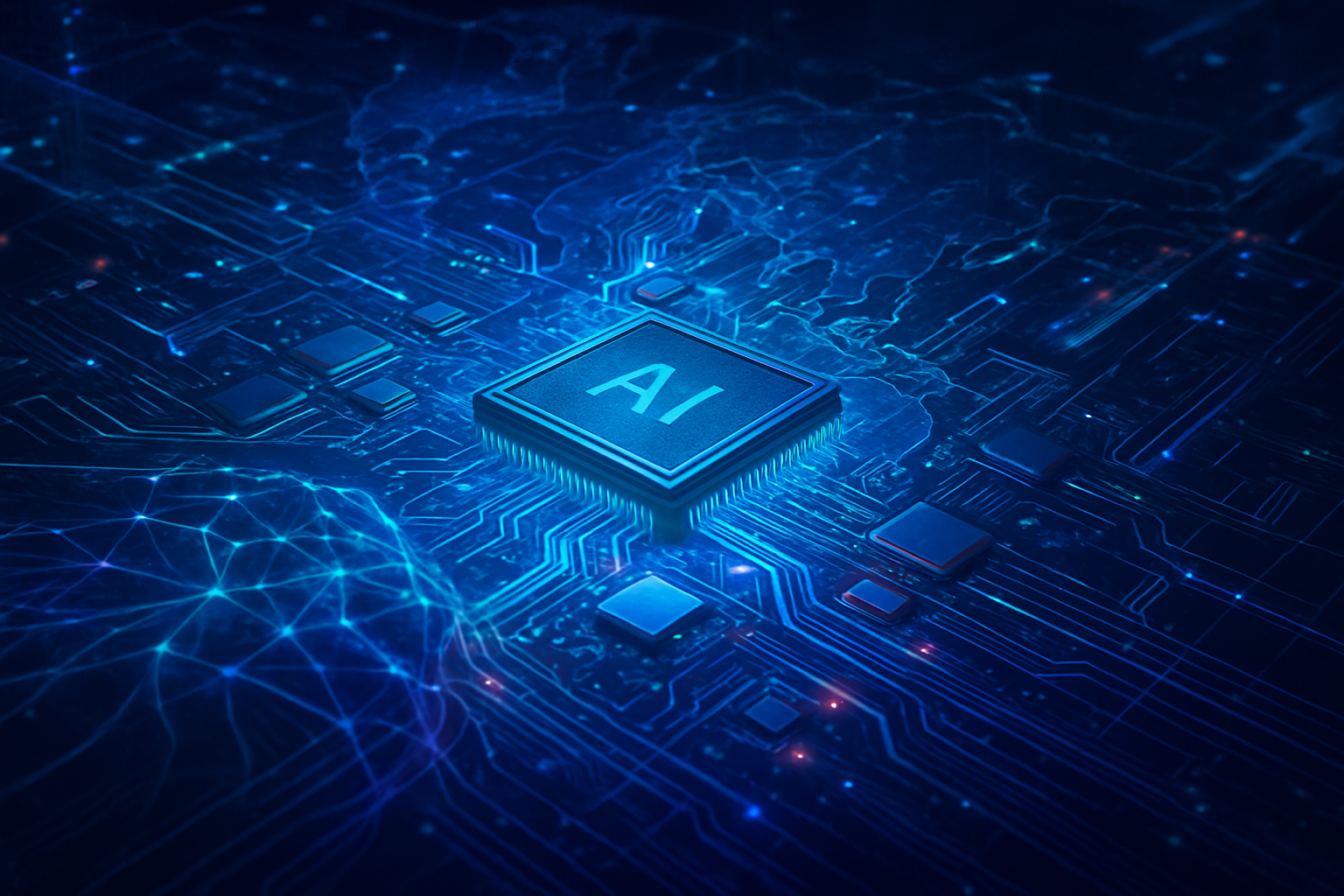
The integration of Monolith AI's capabilities with CoreWeave's (private company) purpose-built, GPU-accelerated AI cloud infrastructure creates a powerful synergy. Traditionally, applying AI to industrial design involved laborious manual data preparation, specialized expertise, and significant computational resources, often leading to fragmented workflows. The combined entity will offer an end-to-end solution where CoreWeave's robust cloud provides the computational backbone for Monolith's physics-informed machine learning. This new approach differs fundamentally from previous methods by embedding advanced AI tools directly into engineering workflows, making AI-driven design accessible to non-specialist engineers. For instance, automotive engineers can predict crash dynamics virtually before physical prototypes are built, and aerospace manufacturers can optimize wing designs based on millions of virtual test cases, significantly reducing the need for costly and time-consuming physical experiments.
Initial reactions from industry experts highlight the transformative potential of this acquisition. Many see it as a validation of AI's growing utility beyond generative models and a strong indicator of the trend towards vertical integration in the AI space. The ability to dramatically shorten R&D cycles, accelerate product development, and unlock new levels of competitive advantage through AI-driven innovation is expected to resonate deeply within the industrial community, which has long sought more efficient ways to tackle complex engineering challenges.
Reshaping the AI Landscape for Enterprises and Innovators
This acquisition is set to have far-reaching implications across the AI industry, benefiting not only CoreWeave and its new industrial clientele but also shaping the competitive dynamics among tech giants and startups. CoreWeave stands to gain a significant strategic advantage by extending its AI cloud platform into a specialized, high-value niche. By offering a full-stack solution from infrastructure to application-specific AI, CoreWeave can cultivate a sticky customer base within industrial sectors, complementing its previous acquisitions like OpenPipe (private company) for reinforcement learning and Weights & Biases (private company) for model iteration.
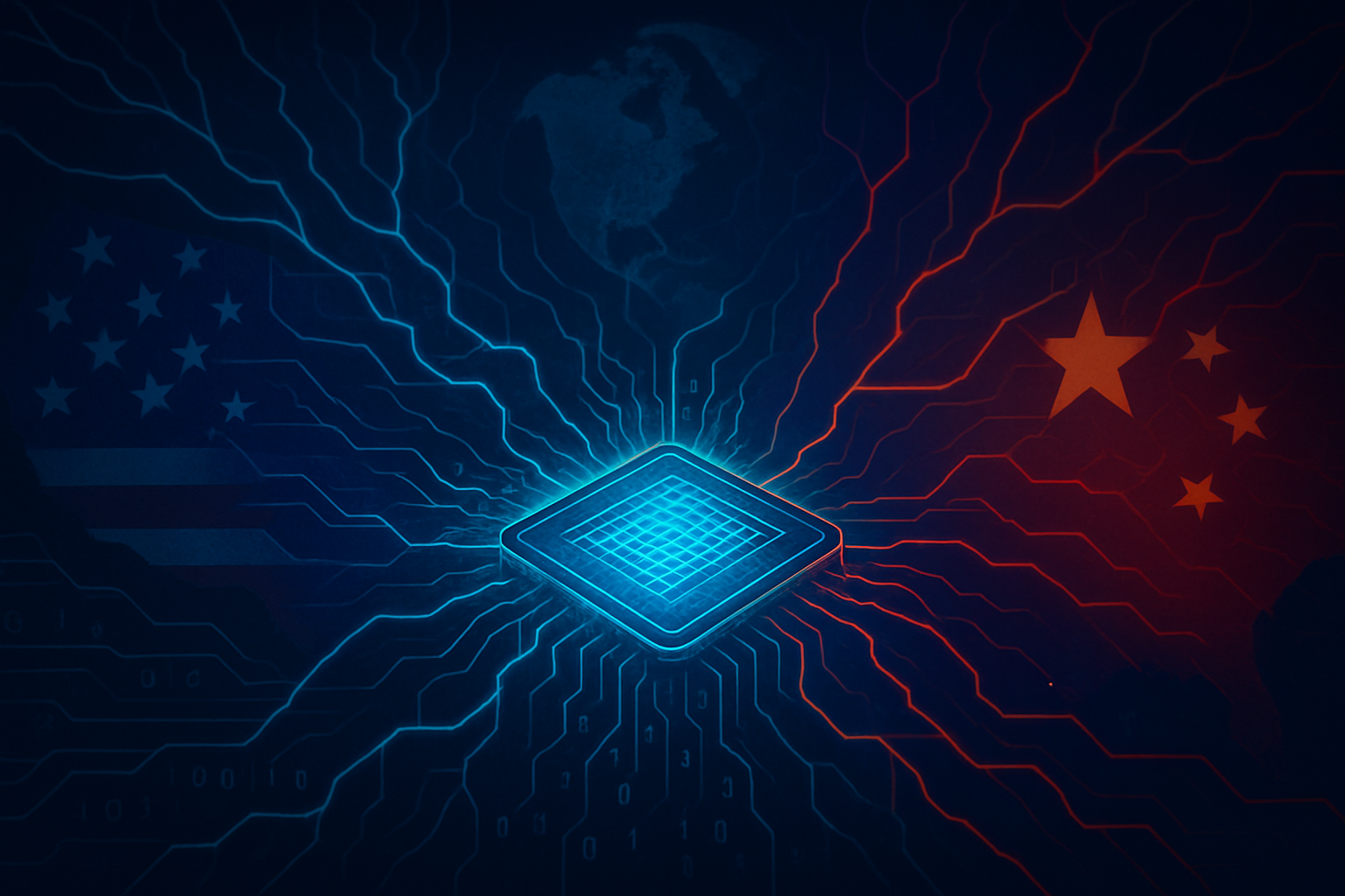
For major AI labs and tech companies, this move by CoreWeave could signal a new front in the AI arms race: the race for vertical integration and domain-specific AI solutions. While many tech giants focus on foundational models and general-purpose AI, CoreWeave's targeted approach with Monolith AI demonstrates the power of specialized, full-stack offerings. This could potentially disrupt existing product development services and traditional engineering software providers that have yet to fully integrate advanced AI into their core offerings. Startups focusing on industrial AI or physics-informed machine learning might find increased interest from investors and potential acquirers, as the market validates the demand for such specialized tools. The competitive landscape will likely see an increased focus on practical, deployable AI solutions that deliver measurable ROI in specific industries.
A Broader Significance for AI's Industrial Revolution
CoreWeave's acquisition of Monolith AI fits squarely into the broader AI landscape's trend towards practical application and vertical specialization. While much of the recent AI hype has centered around large language models and generative AI, this move underscores the critical importance of AI in solving real-world, complex problems in established industries. It signifies a maturation of the AI industry, moving beyond theoretical breakthroughs to tangible, economic impacts. The ability to reduce battery testing by up to 73% or predict crash dynamics virtually before physical prototypes are built represents not just efficiency gains, but a fundamental shift in how products are designed and brought to market.
The impacts are profound: accelerated innovation, reduced costs, and the potential for entirely new product categories enabled by AI-driven design. However, potential concerns, while not immediately apparent from the announcement, could include the need for robust data governance in highly sensitive industrial data, the upskilling of existing engineering workforces, and the ethical implications of AI-driven design decisions. This milestone draws comparisons to earlier AI breakthroughs that democratized access to complex computational tools, such as the advent of CAD/CAM software in the 1980s or simulation tools in the 1990s. This time, AI is not just assisting engineers; it's becoming an integral, intelligent partner in the creative and problem-solving process.
The Horizon: AI-Driven Design and Autonomous Engineering
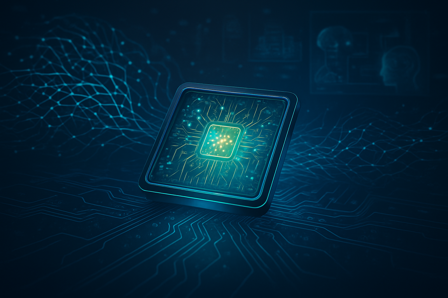
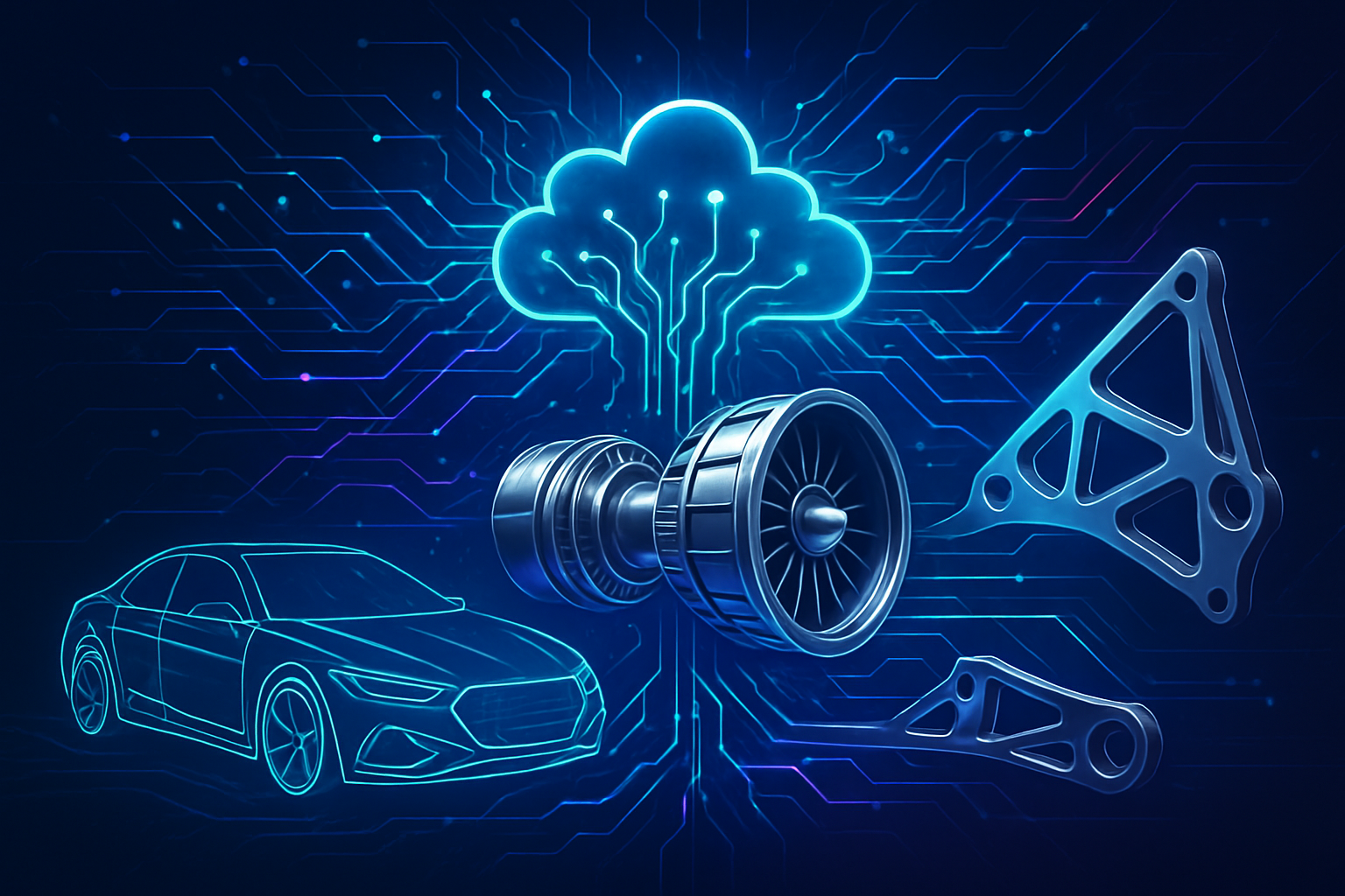
Looking ahead, the integration of CoreWeave and Monolith AI promises a future where AI-driven design becomes the norm, not the exception. In the near term, we can expect to see enhanced capabilities for predictive modeling across a wider range of industrial applications, from material science to advanced robotics. The platform will likely evolve to offer more autonomous design functionalities, where AI can iterate through millions of design possibilities in minutes, optimizing for multiple performance criteria simultaneously. Potential applications include hyper-efficient aerospace components, personalized medical devices, and entirely new classes of sustainable materials.
Long-term developments could lead to fully autonomous engineering cycles, where AI assists from concept generation through to manufacturing optimization with minimal human intervention. Challenges will include ensuring seamless data integration across disparate engineering systems, building trust in AI-generated designs, and continuously advancing the physics-informed AI models to handle ever-greater complexity. Experts predict that this strategic acquisition will accelerate the adoption of AI in heavy industries, fostering a new era of innovation where the speed and scale of AI are harnessed to solve humanity's most pressing engineering and design challenges. The ultimate goal is to enable a future where groundbreaking products can be designed, tested, and brought to market with unprecedented speed and efficiency.
A New Chapter for Industrial AI
CoreWeave's acquisition of Monolith AI marks a significant turning point in the application of artificial intelligence, heralding a new chapter for industrial innovation. The key takeaway is the creation of a vertically integrated, full-stack AI platform designed to empower engineers in sectors like manufacturing, automotive, and aerospace with advanced AI capabilities. This development is not merely an expansion of cloud services; it's a strategic move to embed AI directly into the heart of industrial design and R&D, democratizing access to powerful predictive modeling and simulation tools.
The significance of this development in AI history lies in its clear demonstration that AI's transformative power extends far beyond generative content and large language models. It underscores the immense value of specialized AI solutions tailored to specific industry challenges, paving the way for unprecedented efficiency and innovation in the physical world. As AI continues to mature, such targeted integrations will likely become more common, leading to a more diverse and impactful AI landscape. In the coming weeks and months, the industry will be watching closely to see how CoreWeave integrates Monolith AI's technology, the new offerings that emerge, and the initial successes reported by early adopters in the industrial sector. This acquisition is a testament to AI's burgeoning role as a foundational technology for industrial progress.
This content is intended for informational purposes only and represents analysis of current AI developments.
TokenRing AI delivers enterprise-grade solutions for multi-agent AI workflow orchestration, AI-powered development tools, and seamless remote collaboration platforms.
For more information, visit https://www.tokenring.ai/.