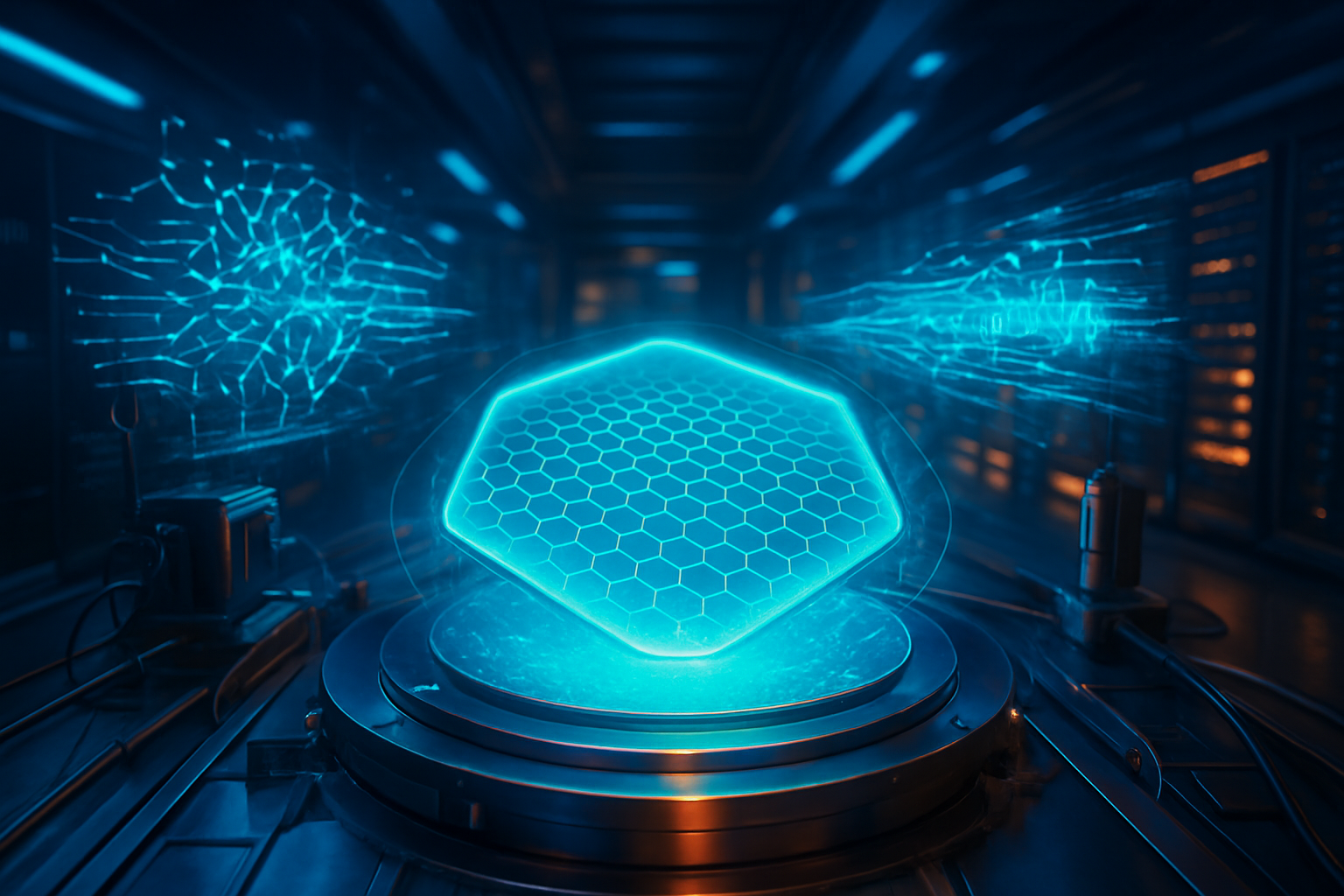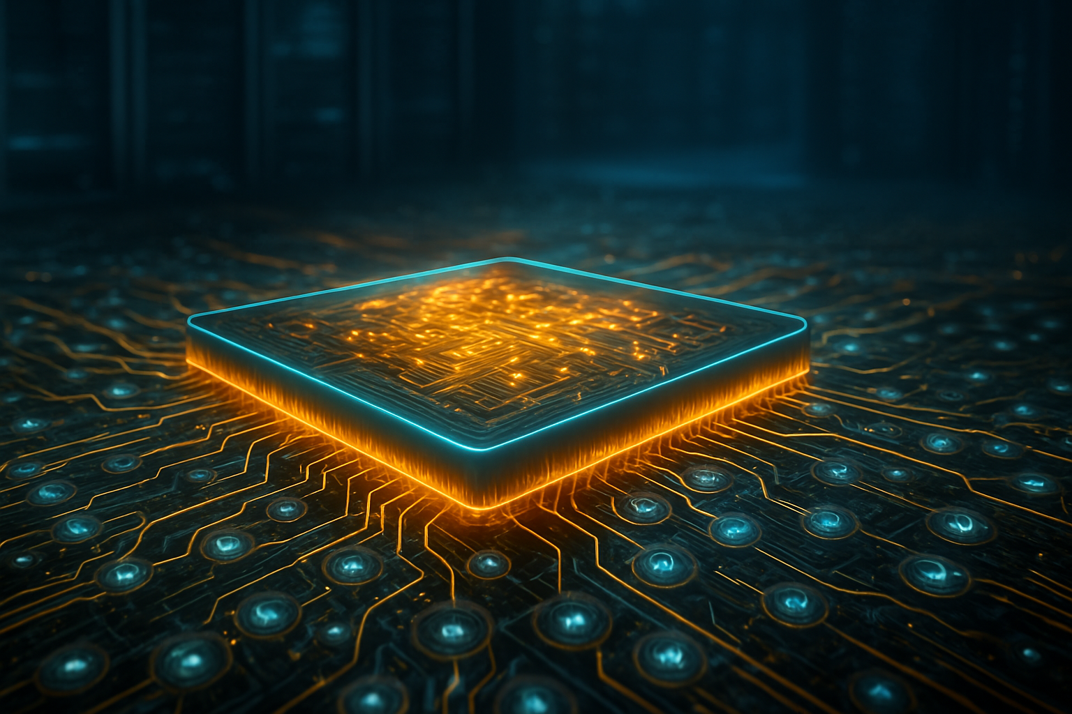
As the global demand for artificial intelligence reaches an atmospheric peak, a revolutionary computing architecture known as Computational RAM (CRAM) is poised to solve the industry’s most persistent bottleneck. By performing calculations directly within the memory cells themselves, CRAM effectively eliminates the "memory wall"—the energy-intensive data transfer between storage and processing—promising an unprecedented 2,500-fold increase in energy efficiency for AI workloads.
This breakthrough, primarily spearheaded by researchers at the University of Minnesota, comes at a critical juncture in January 2026. With AI data centers now consuming electricity at rates comparable to mid-sized nations, the shift from traditional processing to "logic-in-memory" is no longer a theoretical curiosity but a commercial necessity. As the industry moves toward "beyond-CMOS" (Complementary Metal-Oxide-Semiconductor) technologies, CRAM represents the most viable path toward sustainable, high-performance artificial intelligence.
Redefining the Architecture: The End of the Von Neumann Era
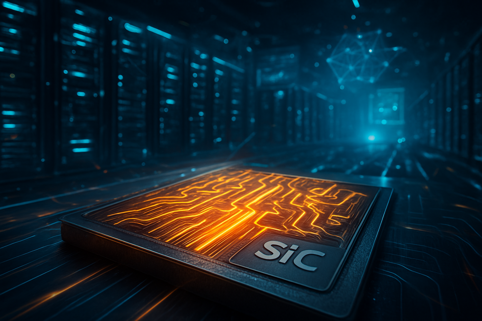
For over 70 years, computing has been defined by the Von Neumann architecture, where the processor (CPU or GPU) and the memory (RAM) are physically separate. In this paradigm, every calculation requires data to be "shuttled" across a bus, a process that consumes roughly 200 times more energy than the computation itself. CRAM disrupts this by utilizing Magnetic Tunnel Junctions (MTJs)—the same spintronic technology used in high-end hard drives—to store data and perform logic operations simultaneously.
Unlike standard RAM that relies on volatile electrical charges, CRAM uses a 2T1M configuration (two transistors and one MTJ). One transistor handles standard memory storage, while the second acts as a switch to enable a "logic mode." By connecting multiple MTJs to a shared Logic Line, the system can perform complex operations like AND, OR, and NOT by simply adjusting voltage pulses. This fully digital approach makes CRAM far more robust and scalable than other "Processing-in-Memory" (PIM) solutions that rely on error-prone analog signals.
Experimental demonstrations published in npj Unconventional Computing have validated these claims, showing that a CRAM-based machine learning accelerator can classify handwritten digits with 2,500x the energy efficiency and 1,700x the speed of traditional near-memory systems. For the broader AI industry, this translates to a consistent 1,000x reduction in energy consumption, a figure that could rewrite the economics of large-scale model training and inference.
The Industrial Shift: Tech Giants and the Search for Sustainability
The move toward CRAM is already drawing significant attention from the semiconductor industry's biggest players. Intel Corporation (NASDAQ: INTC) has been a prominent supporter of the University of Minnesota’s research, viewing spintronics as a primary candidate for the next generation of computing. Similarly, Honeywell International Inc. (NASDAQ: HON) has provided expertise and funding, recognizing the potential for CRAM in high-reliability aerospace and defense applications.
The competitive landscape for AI hardware leaders like NVIDIA Corporation (NASDAQ: NVDA) and Advanced Micro Devices, Inc. (NASDAQ: AMD) is also shifting. While these companies currently dominate the market with HBM4 (High Bandwidth Memory) and advanced GPU architectures to mitigate the memory wall, CRAM represents a disruptive "black swan" technology. If commercialized successfully, it could render current data-transfer-heavy GPU architectures obsolete for specific AI inference tasks. Analysts at the 2026 Consumer Electronics Show (CES) have noted that while HBM4 is the current industry "stopgap," in-memory computing is the long-term endgame for the 2027–2030 roadmap.
For startups, the emergence of CRAM creates a fertile ground for "Edge AI" innovation. Devices that previously required massive batteries or constant tethering to a power source—such as autonomous drones, wearable health monitors, and remote sensors—could soon run sophisticated generative AI models locally using only milliwatts of power.
A Global Imperative: AI Power Consumption and Environmental Impact
The broader significance of CRAM cannot be overstated in the context of global energy policy. As of early 2026, the energy consumption of AI data centers is on track to rival the entire electricity demand of Japan. This "energy wall" has become a geopolitical concern, with tech companies increasingly forced to build their own power plants or modular nuclear reactors to sustain their AI ambitions. CRAM offers a technological "get out of jail free" card by reducing the power footprint of these facilities by three orders of magnitude.
Furthermore, CRAM fits into a larger trend of "non-volatile" computing. Because it uses magnetic states rather than electrical charges to store data, CRAM does not lose information when power is cut. This enables "instant-on" AI systems and "zero-leakage" standby modes, which are critical for the billions of IoT devices expected to populate the global network by 2030.
However, the transition to CRAM is not without concerns. Shifting from traditional CMOS manufacturing to spintronics requires significant changes to existing semiconductor fabrication plants (fabs). There is also the challenge of software integration; the entire stack of modern software, from compilers to operating systems, is built on the assumption of separate memory and logic. Re-coding the world for CRAM will be a monumental task for the global developer community.
The Road to 2030: Commercialization and Future Horizons
Looking ahead, the timeline for CRAM is accelerating. Lead researcher Professor Jian-Ping Wang and the University of Minnesota’s Technology Commercialization office have seen a record-breaking number of startups emerging from their labs in late 2025. Experts predict that the first commercial CRAM chips will begin appearing in specialized industrial sensors and military hardware by 2028, with widespread adoption in consumer electronics and data centers by 2030.
The next major milestone to watch for is the integration of CRAM into a "hybrid" chip architecture, where traditional CPUs handle general-purpose tasks while CRAM blocks act as ultra-efficient AI accelerators. Researchers are also exploring "3D CRAM," which would stack memory layers vertically to provide even higher densities for massive large language models (LLMs).
Despite the hurdles of manufacturing and software compatibility, the consensus among industry leaders is clear: the current path of AI energy consumption is unsustainable. CRAM is not just an incremental improvement; it is a fundamental architectural reset that could ensure the AI revolution continues without exhausting the planet’s energy resources.
Summary of the CRAM Breakthrough
The emergence of Computational RAM marks one of the most significant shifts in computer science history since the invention of the transistor. By performing calculations within memory cells and achieving 2,500x energy efficiency, CRAM addresses the two greatest threats to the AI industry: the physical memory wall and the spiraling cost of energy.
As we move through 2026, the industry should keep a close eye on pilot manufacturing runs and the formation of a "CRAM Standards Consortium" to facilitate software compatibility. While we are still several years away from seeing a CRAM-powered smartphone, the laboratory successes of 2024 and 2025 have paved the way for a more sustainable and powerful future for artificial intelligence.
This content is intended for informational purposes only and represents analysis of current AI developments.
TokenRing AI delivers enterprise-grade solutions for multi-agent AI workflow orchestration, AI-powered development tools, and seamless remote collaboration platforms.
For more information, visit https://www.tokenring.ai/.