Tag: AI

  • The Great Compute Realignment: OpenAI Taps Google TPUs to Power the Future of ChatGPT

    The Great Compute Realignment: OpenAI Taps Google TPUs to Power the Future of ChatGPT

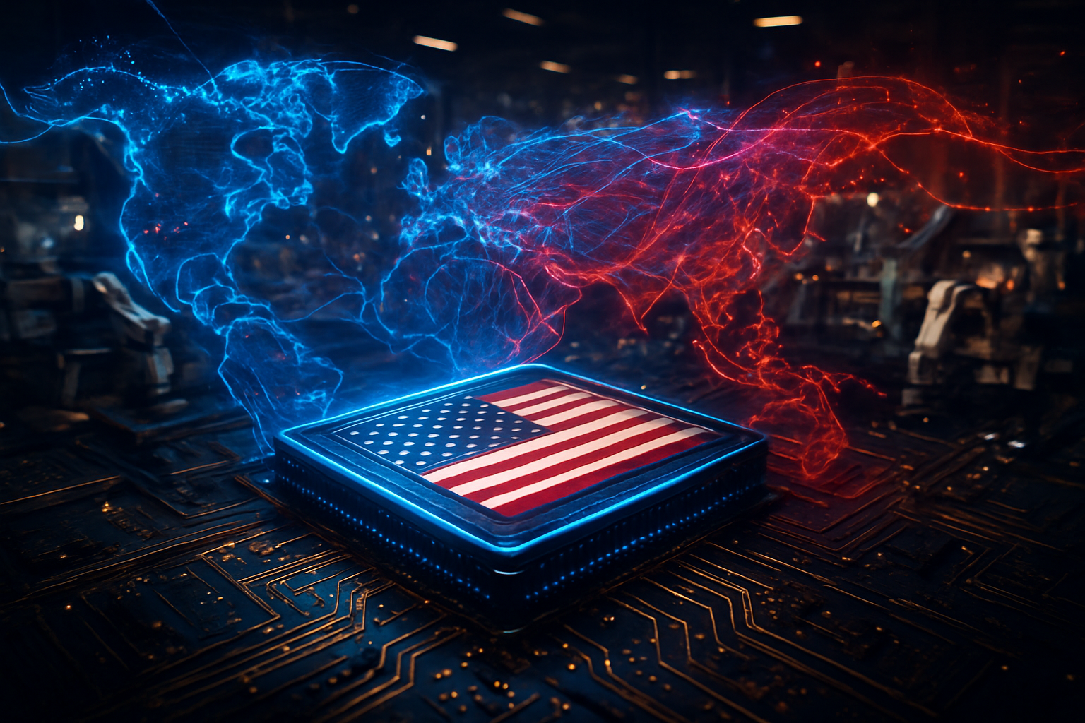
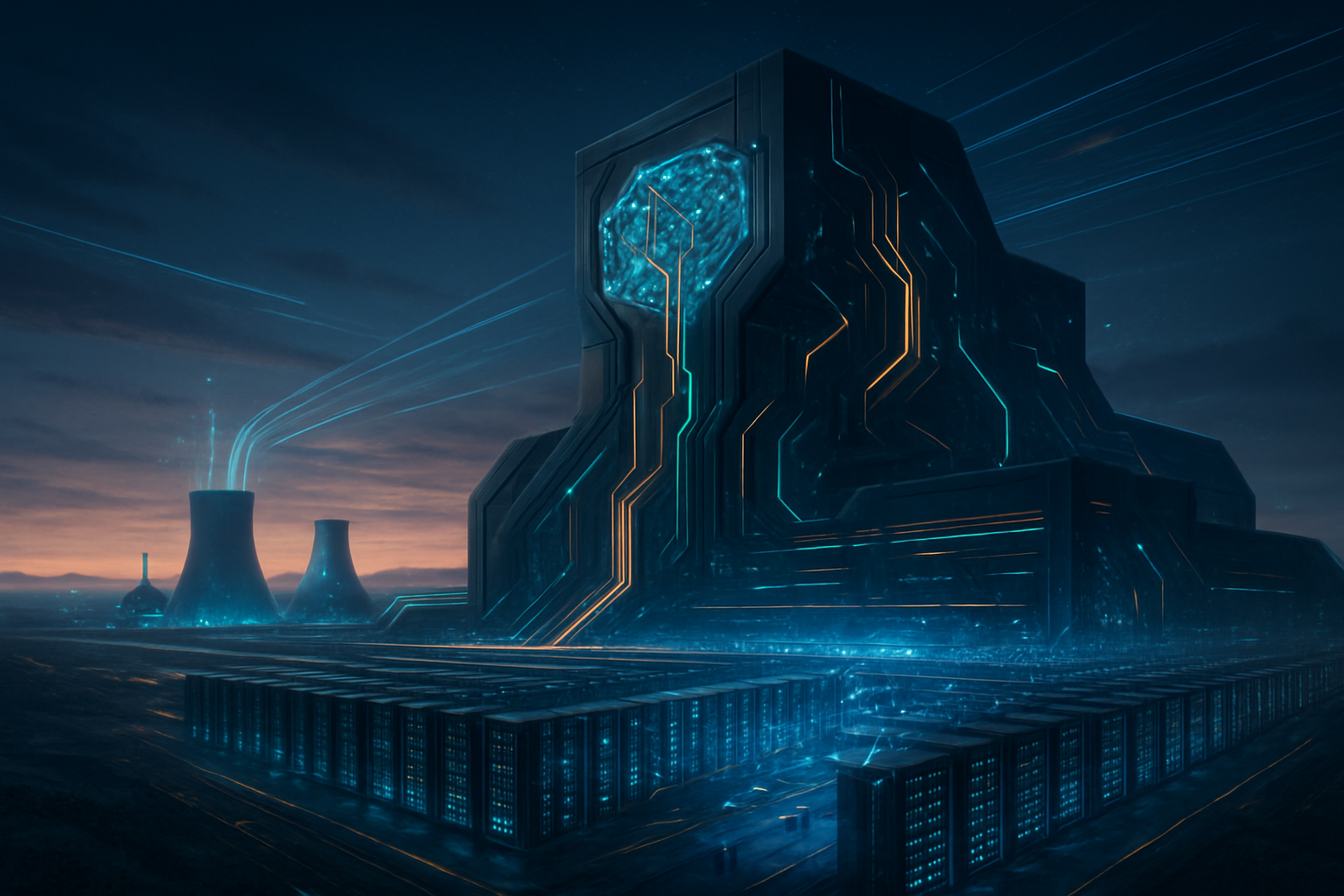
    In a move that has sent shockwaves through the heart of Silicon Valley, OpenAI has officially diversified its massive compute infrastructure, moving a significant portion of ChatGPT’s inference operations onto Google’s (NASDAQ: GOOGL) custom Tensor Processing Units (TPUs). This strategic shift, confirmed in late 2025 and accelerating into early 2026, marks the first time the AI powerhouse has looked significantly beyond its primary benefactor, Microsoft (NASDAQ: MSFT), for the raw processing power required to sustain its global user base of over 700 million monthly active users.

    The partnership represents a fundamental realignment of the AI power structure. By leveraging Google Cloud’s specialized hardware, OpenAI is not only mitigating the "NVIDIA tax" associated with the high cost of H100 and B200 GPUs but is also securing the low-latency capacity necessary for its next generation of "reasoning" models. This transition signals the end of the exclusive era of the OpenAI-Microsoft partnership and underscores a broader industry trend toward hardware diversification and "Silicon Sovereignty."

    The Rise of Ironwood: Technical Superiority and Cost Efficiency

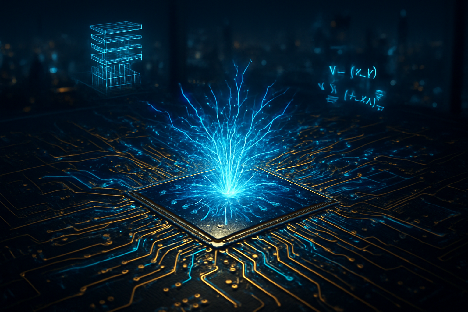
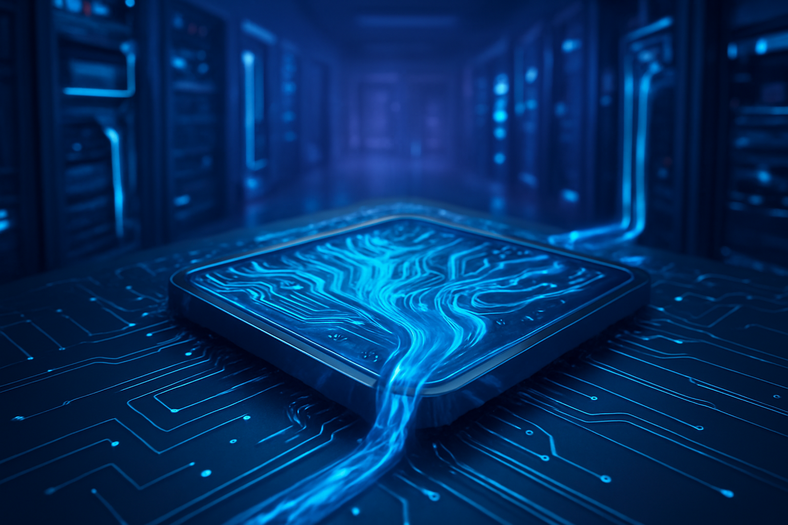
    At the core of this transition is the mass deployment of Google’s 7th-generation TPU, codenamed "Ironwood." Introduced in late 2025, Ironwood was designed specifically for the "Age of Inference"—an era where the cost of running models (inference) has surpassed the cost of training them. Technically, the Ironwood TPU (v7) offers a staggering 4.6 PFLOPS of FP8 peak compute and 192GB of HBM3E memory, providing 7.38 TB/s of bandwidth. This represents a generational leap over the previous Trillium (v6) hardware and a formidable alternative to NVIDIA’s (NASDAQ: NVDA) Blackwell architecture.

    What truly differentiates the TPU stack for OpenAI is Google’s proprietary Optical Circuit Switching (OCS). Unlike traditional Ethernet-based GPU clusters, OCS allows OpenAI to link up to 9,216 chips into a single "Superpod" with 10x lower networking latency. For a model as complex as GPT-4o or the newer o1 "Reasoning" series, this reduction in latency is critical for real-time applications. Industry experts estimate that running inference on Google TPUs is approximately 20% to 40% more cost-effective than using general-purpose GPUs, a vital margin for OpenAI as it manages a burn rate projected to hit $17 billion this year.

    The AI research community has reacted with a mix of surprise and validation. For years, Google’s TPU ecosystem was viewed as a "walled garden" reserved primarily for its own Gemini models. OpenAI’s adoption of the XLA (Accelerated Linear Algebra) compiler—necessary to run code on TPUs—demonstrates that the software hurdles once favoring NVIDIA’s CUDA are finally being cleared by the industry’s most sophisticated engineering teams.

    A Blow to Exclusivity: Implications for Tech Giants

    The immediate beneficiaries of this deal are undoubtedly Google and Broadcom (NASDAQ: AVGO). For Google, securing OpenAI as a tenant on its TPU infrastructure is a massive validation of its decade-long investment in custom AI silicon. It effectively positions Google Cloud as the "clear number two" in AI infrastructure, breaking the narrative that Microsoft Azure was the only viable home for frontier models. Broadcom, which co-designs the TPUs with Google, also stands to gain significantly as the primary architect of the world's most efficient AI accelerators.

    For Microsoft (NASDAQ: MSFT), the development is a nuanced setback. While the "Stargate" project—a $500 billion multi-year infrastructure plan with OpenAI—remains intact, the loss of hardware exclusivity signals a more transactional relationship. Microsoft is transitioning from OpenAI’s sole provider to one of several "sovereign enablers." This shift allows Microsoft to focus more on its own in-house Maia 200 chips and the integration of AI into its software suite (Copilot), rather than just providing the "pipes" for OpenAI’s growth.

    NVIDIA (NASDAQ: NVDA), meanwhile, faces a growing challenge to its dominance in the inference market. While it remains the undisputed king of training with its upcoming Vera Rubin platform, the move by OpenAI and other labs like Anthropic toward custom ASICs (Application-Specific Integrated Circuits) suggests that the high margins NVIDIA has enjoyed may be nearing a ceiling. As the market moves from "scarcity" (buying any chip available) to "efficiency" (building the exact chip needed), specialized hardware like TPUs are increasingly winning the high-volume inference wars.

    Silicon Sovereignty and the New AI Landscape

    This infrastructure pivot fits into a broader global trend known as "Silicon Sovereignty." Major AI labs are no longer content with being at the mercy of hardware allocation cycles or high third-party markups. By diversifying into Google TPUs and planning their own custom silicon, OpenAI is following a path blazed by Apple with its M-series chips: vertical integration from the transistor to the transformer.

    The move also highlights the massive scale of the "AI Factories" now being constructed. OpenAI’s projected compute spending is set to jump to $35 billion by 2027. This scale is so vast that it requires a multi-vendor strategy to ensure supply chain resilience. No single company—not even Microsoft or NVIDIA—can provide the 10 gigawatts of power and the millions of chips OpenAI needs to achieve its goals for Artificial General Intelligence (AGI).

    However, this shift raises concerns about market consolidation. Only a handful of companies have the capital and the engineering talent to design and deploy custom silicon at this level. This creates a widening "compute moat" that may leave smaller startups and academic institutions unable to compete with the "Sovereign Labs" like OpenAI, Google, and Meta. Comparisons are already being drawn to the early days of the cloud, where a few dominant players captured the vast majority of the infrastructure market.

    The Horizon: Project Titan and Beyond

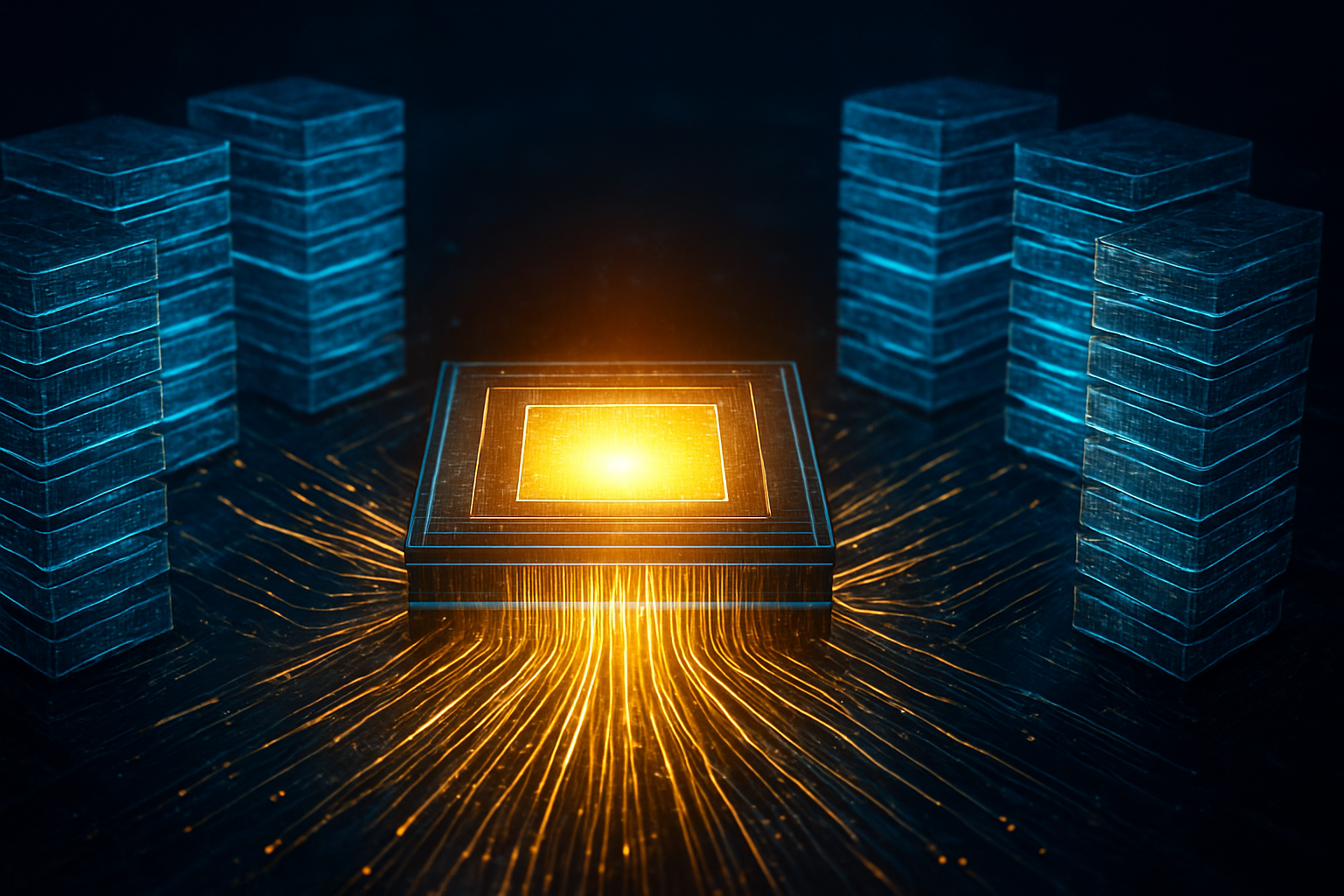
    Looking forward, the use of Google TPUs is likely a bridge to OpenAI’s ultimate goal: "Project Titan." This in-house initiative, partnered with Broadcom and TSMC, aims to produce OpenAI’s own custom inference accelerators by late 2026. These chips will reportedly be tuned specifically for "reasoning-heavy" workloads, where the model performs thousands of internal "thought" steps before generating an answer.

    As these custom chips go live, we can expect to see a new generation of AI applications that were previously too expensive to run at scale. This includes persistent AI agents that can work for hours on complex coding or research tasks, and more seamless, real-time multimodal experiences. The challenge will be managing the immense power requirements of these "AI Factories," with experts predicting that the industry will increasingly turn toward nuclear and other dedicated clean energy sources to fuel their 10GW targets.

    In the near term, we expect OpenAI to continue scaling its footprint in Google Cloud regions globally, particularly those with the newest Ironwood TPU clusters. This will likely be accompanied by a push for more efficient model architectures, such as Mixture-of-Experts (MoE), which are perfectly suited for the distributed memory architecture of the TPU Superpods.

    Conclusion: A Turning Point in AI History

    The decision by OpenAI to rent Google TPUs is more than a simple procurement deal; it is a landmark event in the history of artificial intelligence. It marks the transition of the industry from a hardware-constrained "gold rush" to a mature, efficiency-driven infrastructure era. By breaking the GPU monopoly and diversifying its compute stack, OpenAI has taken a massive step toward long-term sustainability and operational independence.

    The key takeaways for the coming months are clear: watch for the performance benchmarks of the Ironwood TPU v7 as it scales, monitor the progress of OpenAI’s "Project Titan" with Broadcom, and observe how Microsoft responds to this newfound competition within its own backyard. As of January 2026, the message is loud and clear: the future of AI will not be built on a single architecture, but on a diverse, competitive, and highly specialized silicon landscape.


    This content is intended for informational purposes only and represents analysis of current AI developments.

    TokenRing AI delivers enterprise-grade solutions for multi-agent AI workflow orchestration, AI-powered development tools, and seamless remote collaboration platforms.
    For more information, visit https://www.tokenring.ai/.

  • Trump Administration Slaps 25% Tariffs on High-End NVIDIA and AMD AI Chips to Force US Manufacturing

    Trump Administration Slaps 25% Tariffs on High-End NVIDIA and AMD AI Chips to Force US Manufacturing

    In a move that marks the most aggressive shift in global technology trade policy in decades, President Trump signed a national security proclamation yesterday, January 14, 2026, imposing a 25% tariff on the world’s most advanced artificial intelligence semiconductors. The order specifically targets NVIDIA (NASDAQ: NVDA) and AMD (NASDAQ: AMD), hitting their flagship H200 and Instinct MI325X chips. This "Silicon Surcharge" is designed to act as a financial hammer, forcing these semiconductor giants to move their highly sensitive advanced packaging and fabrication processes from Taiwan to the United States.

    The immediate significance of this order cannot be overstated. By targeting the H200 and MI325X—the literal engines of the generative AI revolution—the administration is signaling that "AI Sovereignty" now takes precedence over corporate margins. While the administration has framed the move as a necessary step to mitigate the national security risks of offshore fabrication, the tech industry is bracing for a massive recalibration of supply chains. Analysts suggest that the tariffs could add as much as $12,000 to the cost of a single high-end AI GPU, fundamentally altering the economics of data center builds and AI model training overnight.

    The Technical Battleground: H200, MI325X, and the Packaging Bottleneck

    The specific targeting of NVIDIA’s H200 and AMD’s MI325X is a calculated strike at the "gold standard" of AI hardware. The NVIDIA H200, built on the Hopper architecture, features 141GB of HBM3e memory and is the primary workhorse for large language model (LLM) inference. Its rival, the AMD Instinct MI325X, boasts an even larger 256GB of usable HBM3e memory, making it a critical asset for researchers handling massive datasets. Until now, both chips have relied almost exclusively on Taiwan Semiconductor Manufacturing Company (NYSE: TSM) for fabrication using 4nm and 5nm process nodes, and perhaps more importantly, for "CoWoS" (Chip-on-Wafer-on-Substrate) advanced packaging.

    This order differs from previous trade restrictions by moving away from the "blanket bans" of the early 2020s toward a "revenue-capture" model. By allowing the sale of these chips but taxing them at 25%, the administration is effectively creating a state-sanctioned toll road for advanced silicon. Initial reactions from the AI research community have been a mixture of shock and pragmatism. While some researchers at labs like OpenAI and Anthropic worry about the rising cost of compute, others acknowledge that the policy provides a clearer, albeit more expensive, path to acquiring hardware that was previously caught in a web of export-control uncertainty.

    Winners, Losers, and the "China Pivot"

    The implications for industry titans are profound. NVIDIA (NASDAQ: NVDA) and AMD (NASDAQ: AMD) now face a complex choice: pass the 25% tariff costs onto customers or accelerate their multi-billion dollar transitions to domestic facilities. Intel (NASDAQ: INTC) stands to benefit significantly from this shift; as the primary domestic alternative with established fabrication and growing packaging capabilities in Ohio and Arizona, Intel may see a surge in interest for its Gaudi-line of accelerators if it can close the performance gap with NVIDIA.

    For cloud giants like Amazon (NASDAQ: AMZN), Google (NASDAQ: GOOGL), and Microsoft (NASDAQ: MSFT), the tariffs represent a massive increase in capital expenditure for their international data centers. However, a crucial "Domestic Exemption" in the order ensures that chips imported specifically for use in U.S.-based data centers may be eligible for rebates, further incentivizing the concentration of AI power within American borders. Perhaps the most controversial aspect of the order is the "China Pivot"—a policy reversal that allows NVIDIA and AMD to sell H200-class chips to Chinese firms, provided the 25% tariff is paid directly to the U.S. Treasury and domestic U.S. demand is fully satisfied first.

    A New Era of Geopolitical AI Fragmentation

    This development fits into a broader trend of "technological decoupling" and the rise of a two-tier global AI market. By leveraging tariffs, the U.S. is effectively subsidizing its own domestic manufacturing through the fees collected from international sales. This marks a departure from the "CHIPS Act" era of direct subsidies, moving instead toward a more protectionist stance where access to the American AI ecosystem is the ultimate leverage. The 25% tariff essentially creates a "Trusted Tier" of hardware for the U.S. and its allies, and a "Taxed Tier" for the rest of the world.

    Comparisons are already being drawn to the 1980s semiconductor wars with Japan, but the stakes today are vastly higher. Critics argue that these tariffs could slow the global pace of AI innovation by making the necessary hardware prohibitively expensive for startups in Europe and the Global South. Furthermore, there are concerns that this move could provoke retaliatory measures from China, such as restricting the export of rare earth elements or the HBM (High Bandwidth Memory) components produced by firms like SK Hynix that are essential for these very chips.

    The Road to Reshoring: What Comes Next?

    In the near term, the industry is looking toward the completion of advanced packaging facilities on U.S. soil. Amkor Technology (NASDAQ: AMKR) and TSMC (NYSE: TSM) are both racing to finish high-end packaging plants in Arizona by late 2026. Once these facilities are operational, NVIDIA and AMD will likely be able to bypass the 25% tariff by certifying their chips as "U.S. Manufactured," a transition the administration hopes will create thousands of high-tech jobs and secure the AI supply chain against a potential conflict in the Taiwan Strait.

    Experts predict that we will see a surge in "AI hardware arbitrage," where secondary markets attempt to shuffle chips between jurisdictions to avoid the Silicon Surcharge. In response, the U.S. Department of Commerce is expected to roll out a "Silicon Passport" system—a blockchain-based tracking mechanism to ensure every H200 and MI325X chip can be traced from the fab to the server rack. The next six months will be a period of intense lobbying and strategic realignment as tech companies seek to define what exactly constitutes "U.S. Manufacturing" under the new rules.

    Summary and Final Assessment

    The Trump Administration’s 25% tariff on NVIDIA and AMD chips represents a watershed moment in the history of the digital age. By weaponizing the supply chain of the most advanced silicon on earth, the U.S. is attempting to forcefully repatriate an industry that has been offshore for decades. The key takeaways are clear: the cost of global AI compute is going up, the "China Ban" is being replaced by a "China Tax," and the pressure on semiconductor companies to build domestic capacity has reached a fever pitch.

    In the long term, this move may be remembered as the birth of true "Sovereign AI," where a nation’s power is measured not just by its algorithms, but by the physical silicon it can forge within its own borders. Watch for the upcoming quarterly earnings calls from NVIDIA and AMD in the weeks ahead; their guidance on "tariff-adjusted pricing" will provide the first real data on how the market intends to absorb this seismic policy shift.


    This content is intended for informational purposes only and represents analysis of current AI developments.

    TokenRing AI delivers enterprise-grade solutions for multi-agent AI workflow orchestration, AI-powered development tools, and seamless remote collaboration platforms.
    For more information, visit https://www.tokenring.ai/.

  • TSMC Sets Historic $56 Billion Capex for 2026 to Accelerate 2nm and A16 Production

    TSMC Sets Historic $56 Billion Capex for 2026 to Accelerate 2nm and A16 Production

    The Angstrom Era Begins: TSMC Shatters Records with $56 Billion Capex to Scale 2nm and A16 Production

    In a move that has sent shockwaves through the global technology sector, Taiwan Semiconductor Manufacturing Company (NYSE: TSM) announced today during its Q4 2025 earnings call that it will raise its capital expenditure (capex) budget to a staggering $52 billion to $56 billion for 2026. This massive financial commitment marks a significant escalation from the $40.9 billion spent in 2025, signaling the company's aggressive pivot to dominate the next generation of artificial intelligence and high-performance computing silicon.

    The announcement comes as the "AI Giga-cycle" reaches a fever pitch, with cloud providers and sovereign states demanding unprecedented levels of compute power. By allocating 70-80% of this record-breaking budget to its 2nm (N2) and A16 (1.6nm) roadmaps, TSMC is positioning itself as the sole gateway to the "angstrom era"—a transition in semiconductor manufacturing where features are measured in units smaller than a nanometer. This investment is not just a capacity expansion; it is a strategic moat designed to secure TSMC’s role as the primary forge for the world's most advanced AI accelerators and consumer electronics.

    The Architecture of Tomorrow: From Nanosheets to Super Power Rails

    The technical cornerstone of TSMC’s $56 billion investment lies in its transition from the long-standing FinFET transistor architecture to Nanosheet Gate-All-Around (GAA) technology. The 2nm process, internally designated as N2, entered volume production in late 2025, but the 2026 budget focuses on the rapid ramp-up of N2P and N2X—high-performance variants optimized for AI data centers. Compared to the current 3nm (N3P) standard, the N2 node offers a 15% speed improvement at the same power levels or a 30% reduction in power consumption, providing the thermal headroom necessary for the next generation of energy-hungry AI chips.

    Even more ambitious is the A16 process, representing the 1.6nm node. TSMC has confirmed that A16 will integrate its proprietary "Super Power Rail" (SPR) technology, which implements backside power delivery. By moving the power distribution network to the back of the silicon wafer, TSMC can drastically reduce voltage drop and interference, allowing for more efficient power routing to the billions of transistors on a single die. This architecture is expected to provide an additional 10% performance boost over N2P, making it the most sophisticated logic technology ever planned for mass production.

    Industry experts have reacted with a mix of awe and caution. While the technical specifications of A16 and N2 are unmatched, the sheer scale of the investment highlights the increasing difficulty of "Moores Law" scaling. The research community notes that TSMC is successfully navigating the transition to GAA transistors, an area where competitors like Samsung (KRX: 005930) and Intel (NASDAQ: INTC) have historically faced yield challenges. By doubling down on these advanced nodes, TSMC is betting that its "Golden Yield" reputation will allow it to capture nearly the entire market for sub-2nm chips.

    A High-Stakes Land Grab: Apple, NVIDIA, and the Fight for Capacity

    This record-breaking capex budget is essentially a response to a "land grab" for semiconductor capacity by the world's tech titans. Apple (NASDAQ: AAPL) has already secured its position as the lead customer for the N2 node, which is expected to power the A20 chip in the upcoming iPhone 18 and the M5-series processors for Mac. Apple’s early adoption provides TSMC with a stable, high-volume baseline, allowing the foundry to refine its 2nm yields before opening the floodgates for other high-performance clients.

    For NVIDIA (NASDAQ: NVDA), the 2026 expansion is a critical lifeline. Reports indicate that NVIDIA has secured exclusive early access to the A16 process for its next-generation "Feynman" GPU architecture, rumored for a 2027 release. As NVIDIA moves beyond its current Blackwell and Rubin architectures, the move to 1.6nm is seen as essential for maintaining its lead in AI training and inference. Simultaneously, AMD (NASDAQ: AMD) is aggressively pursuing N2P capacity for its EPYC "Zen 6" server CPUs and Instinct MI400 accelerators, as it attempts to close the performance gap with NVIDIA in the data center.

    The strategic advantage for these companies cannot be overstated. By locking in TSMC's 2026 capacity, these giants are effectively pricing out smaller competitors and startups. The massive capex also includes a significant portion—roughly 10-20%—allocated to advanced packaging technologies like CoWoS (Chip-on-Wafer-on-Substrate) and SoIC (System on Integrated Chips). This specialized packaging is currently the primary bottleneck for AI chip production, and TSMC’s expansion of these facilities will directly determine how many H200 or MI300-class chips can be shipped to global markets in the coming years.

    The Global AI Landscape and the "Giga Cycle"

    TSMC’s $56 billion budget is a bellwether for the broader AI landscape, confirming that the industry is in the midst of an unprecedented "Giga Cycle" of infrastructure spending. This isn't just about faster smartphones; it’s about a fundamental shift in global compute requirements. The massive investment suggests that TSMC sees the AI boom as a long-term structural change rather than a short-term bubble. The move contrasts sharply with previous industry cycles, which were often characterized by cyclical oversupply; currently, the demand for AI silicon appears to be outstripping even the most aggressive projections.

    However, this dominance comes with its own set of concerns. TSMC’s decision to implement a 3-5% price hike on sub-5nm wafers in 2026 demonstrates its immense pricing power. As the cost of leading-edge design and manufacturing continues to skyrocket, there is a growing risk that only the largest "Trillion Dollar" companies will be able to afford the transition to the angstrom era. This could lead to a consolidation of AI power, where the most capable models are restricted to those who can pay for the most expensive silicon.

    Furthermore, the geopolitical dimension of this expansion remains a focal point. A portion of the 2026 budget is earmarked for TSMC’s "Gigafab" expansion in Arizona, where the company is already operating its first 4nm plant. By early 2026, TSMC is expected to begin construction on a fourth Arizona facility and its first US-based advanced packaging plant. This geographic diversification is intended to mitigate risks associated with regional tensions in the Taiwan Strait, providing a more resilient supply chain for US-based tech giants like Microsoft (NASDAQ: MSFT) and Google (NASDAQ: GOOGL).

    The Path to 1.4nm and Beyond

    Looking toward the future, the 2026 capex plan provides the roadmap for the rest of the decade. While the focus is currently on 2nm and 1.6nm, TSMC has already begun preliminary research on the A14 (1.4nm) node, which is expected to debut near 2028. The industry is watching closely to see if the physics of silicon scaling will finally hit a "hard wall" or if new materials and architectures, such as carbon nanotubes or further iterations of 3D chip stacking, will keep the performance gains coming.

    In the near term, the most immediate challenge for TSMC will be managing the sheer complexity of the A16 ramp-up. The introduction of Super Power Rail technology requires entirely new design tools and EDA (Electronic Design Automation) software updates. Experts predict that the next 12 to 18 months will be a period of intensive collaboration between TSMC and its "ecosystem partners" like Cadence and Synopsys to ensure that chip designers can actually utilize the density gains promised by the 1.6nm process.

    Final Assessment: The Uncontested King of Silicon

    TSMC's historic $56 billion commitment for 2026 is a definitive statement of intent. By outspending its nearest rivals and pushing the boundaries of physics with N2 and A16, the company is ensuring that the global AI revolution remains fundamentally dependent on Taiwanese technology. The key takeaway for investors and industry observers is that the barrier to entry for leading-edge semiconductor manufacturing has never been higher, and TSMC is the only player currently capable of scaling these "angstrom-era" technologies at the volumes required by the market.

    In the coming weeks, all eyes will be on how competitors like Intel respond to this massive spending increase. While Intel’s "five nodes in four years" strategy has shown promise, TSMC’s record-shattering budget suggests they have no intention of ceding the crown. As we move further into 2026, the success of the 2nm ramp-up will be the primary metric for the health of the entire tech ecosystem, determining the pace of AI advancement for years to come.


    This content is intended for informational purposes only and represents analysis of current AI developments.

    TokenRing AI delivers enterprise-grade solutions for multi-agent AI workflow orchestration, AI-powered development tools, and seamless remote collaboration platforms.
    For more information, visit https://www.tokenring.ai/.

  • TSMC Post Record-Breaking Q4 Profits as AI Demand Hits New Fever Pitch

    TSMC Post Record-Breaking Q4 Profits as AI Demand Hits New Fever Pitch

    Taiwan Semiconductor Manufacturing Co. (NYSE: TSM) has shattered financial records, reporting a net profit of US$16 billion for the fourth quarter of 2025—a 35% year-over-year increase. The blowout results were driven by unrelenting demand for AI accelerators and the rapid ramp-up of 3nm and 5nm technologies, which now account for 63% of the company's total wafer revenue. CEO C.C. Wei confirmed that the 'AI gold rush' continues to fuel high utilization rates across all advanced fabs, solidifying TSMC's role as the indispensable backbone of the global AI economy.

    The financial surge marks a historic milestone for the foundry giant, as revenue from High-Performance Computing (HPC) and AI applications now officially accounts for 55% of the company's total intake, significantly outpacing the smartphone segment for the first time. As the world transitions into a new era of generative AI, TSMC’s quarterly performance serves as a primary bellwether for the entire tech sector, signaling that the infrastructure build-out for artificial intelligence is accelerating rather than cooling off.

    Scaling the Silicon Frontier: 3nm Dominance and the CoWoS Breakthrough

    At the heart of TSMC’s record-breaking quarter is the massive commercial success of its N3 (3nm) and N5 (5nm) process nodes. The 3nm family alone contributed 28% of total wafer revenue in Q4 2025, a steep climb from previous quarters as major clients migrated their flagship products to the more efficient node. This transition represents a significant technical leap over the 5nm generation, offering up to 15% better performance at the same power levels or a 30% reduction in power consumption. These specifications have become critical for AI data centers, where energy efficiency is the primary constraint on scaling massive LLM (Large Language Model) clusters.

    Beyond traditional wafer fabrication, TSMC has successfully navigated the "packaging crunch" that plagued the industry throughout 2024. The company’s Chip-on-Wafer-on-Substrate (CoWoS) advanced packaging capacity—a prerequisite for high-bandwidth memory integration in AI chips—has doubled over the last year to approximately 80,000 wafers per month. This expansion has been vital for the delivery of next-generation accelerators like the Blackwell series from NVIDIA (NASDAQ: NVDA). Industry experts note that TSMC’s ability to integrate advanced lithography with sophisticated 3D packaging is what currently separates it from competitors like Samsung and Intel (NASDAQ: INTC).

    The quarter also saw the official commencement of 2nm (N2) mass production at TSMC’s Hsinchu and Kaohsiung facilities. Unlike the FinFET transistors used in previous nodes, the 2nm process utilizes Nanosheet (GAAFET) architecture, allowing for finer control over current flow and further reducing leakage. Initial yields are reportedly ahead of schedule, with research analysts suggesting that the "AI gold rush" has provided TSMC with the necessary capital to accelerate this transition faster than any previous node shift in the company's history.

    The Kingmaker: Impact on Big Tech and the Fabless Ecosystem

    TSMC’s dominance has created a unique market dynamic where the company acts as the ultimate gatekeeper for the AI industry. Major clients, including NVIDIA, Apple (NASDAQ: AAPL), and Advanced Micro Devices (NASDAQ: AMD), are currently in a high-stakes competition to secure "golden wafers" for 2026 and 2027. NVIDIA, which is projected to become TSMC’s largest customer by revenue in the coming year, has reportedly secured nearly 60% of all available CoWoS output for its upcoming Rubin architecture, leaving rivals and hyperscalers to fight for the remaining capacity.

    This supply-side dominance provides a strategic advantage to "Early Adopters" like Apple, which has utilized its massive capital reserves to lock in 2nm capacity for its upcoming A19 and M5 chips. For smaller AI startups and specialized chipmakers, the barrier to entry is rising. With TSMC’s advanced node capacity essentially pre-sold through 2027, the "haves" of the AI world—those with established TSMC allocations—are pulling further ahead of the "have-nots." This has led to a surge in strategic partnerships and long-term supply agreements as companies seek to avoid the crippling shortages seen in early 2024.

    The competitive landscape is also shifting for TSMC’s foundry rivals. While Intel has made strides with its 18A node, TSMC’s Q4 results suggest that the scale of its ecosystem remains its greatest moat. The "Foundry 2.0" model, as CEO C.C. Wei describes it, integrates manufacturing, advanced packaging, and testing into a single, seamless pipeline. This vertical integration has made it difficult for competitors to lure away high-margin AI clients who require the guaranteed reliability of TSMC’s proven high-volume manufacturing.

    The Backbone of the Global AI Economy

    TSMC’s $16 billion profit is more than just a corporate success story; it is a reflection of the broader geopolitical and economic significance of semiconductors in 2026. The shift in revenue mix toward HPC/AI underscores the reality that "Sovereign AI"—nations building their own localized AI infrastructure—is becoming a primary driver of global demand. From the United States to Europe and the Middle East, governments are subsidizing data center builds that rely almost exclusively on the silicon produced in TSMC’s Taiwan-based fabs.

    The wider significance of this milestone also touches on the environmental impact of AI. As the industry faces criticism over the energy consumption of data centers, the rapid adoption of 3nm and the impending move to 2nm are seen as the only viable path to sustainable AI. By packing more transistors into the same area with lower voltage requirements, TSMC is effectively providing the "efficiency dividends" necessary to keep the AI revolution from overwhelming global power grids. This technical necessity has turned TSMC into a critical pillar of global ESG goals, even as its own power consumption rises to meet production demands.

    Comparisons to previous AI milestones are striking. While the release of ChatGPT in 2022 was the "software moment" for AI, TSMC’s Q4 2025 results mark the "hardware peak." The sheer volume of capital being funneled into advanced nodes suggests that the industry has moved past the experimental phase and is now in a period of heavy industrialization. Unlike the "dot-com" bubble, this era is characterized by massive, tangible hardware investments that are already yielding record profits for the infrastructure providers.

    The Road to 1.6nm: What Lies Ahead

    Looking toward the future, the momentum shows no signs of slowing. TSMC has already announced a massive capital expenditure budget of $52–$56 billion for 2026, aimed at further expanding its footprint in Arizona, Japan, and Germany. The focus is now shifting toward the A16 (1.6nm) process, which is slated for volume production in the second half of 2026. This node will introduce "Super Power Rail" technology—a backside power delivery system that decouples power routing from signal routing, significantly boosting efficiency and performance for AI logic.

    Experts predict that the next major challenge for TSMC will be managing the "complexity wall." As transistors shrink toward the atomic scale, the cost of design and manufacturing continues to skyrocket. This may lead to a more modular future, where "chiplets" from different process nodes are combined using TSMC’s SoIC (System-on-Integrated-Chips) technology. This would allow customers to use expensive 2nm logic only where necessary, while utilizing 5nm or 7nm for less critical components, potentially easing the demand on the most advanced nodes.

    Furthermore, the integration of silicon photonics into the packaging process is expected to be the next major breakthrough. As AI models grow, the bottleneck is no longer just how fast a chip can think, but how fast chips can talk to each other. TSMC’s research into CPO (Co-Packaged Optics) is expected to reach commercial viability by late 2026, potentially enabling a 10x increase in data transfer speeds between AI accelerators.

    Conclusion: A New Era of Silicon Supremacy

    TSMC’s Q4 2025 earnings represent a definitive statement: the AI era is not a speculative bubble, but a fundamental restructuring of the global technology landscape. By delivering a $16 billion profit and scaling 3nm and 5nm nodes to dominate 63% of its revenue, the company has proven that it is the heartbeat of modern computing. CEO C.C. Wei’s "AI gold rush" is more than a metaphor; it is a multi-billion dollar reality that is reshaping every industry from healthcare to high finance.

    As we move further into 2026, the key metrics to watch will be the 2nm ramp-up and the progress of TSMC’s overseas expansion. While geopolitical tensions remain a constant background noise, the world’s total reliance on TSMC’s advanced nodes has created a "silicon shield" that makes the company’s stability a matter of global economic security. For now, TSMC stands alone at the top of the mountain, the essential architect of the intelligence age.


    This content is intended for informational purposes only and represents analysis of current AI developments.

    TokenRing AI delivers enterprise-grade solutions for multi-agent AI workflow orchestration, AI-powered development tools, and seamless remote collaboration platforms.
    For more information, visit https://www.tokenring.ai/.

  • The Silicon Brain: NVIDIA’s BlueField-4 and the Dawn of the Agentic AI Chip Era

    The Silicon Brain: NVIDIA’s BlueField-4 and the Dawn of the Agentic AI Chip Era

    In a move that signals the definitive end of the "chatbot era" and the beginning of the "autonomous agent era," NVIDIA (NASDAQ: NVDA) has officially unveiled its new BlueField-4 Data Processing Unit (DPU) and the underlying Vera Rubin architecture. Announced this month at CES 2026, these developments represent a radical shift in how silicon is designed, moving away from raw mathematical throughput and toward hardware capable of managing the complex, multi-step reasoning cycles and massive "stateful" memory required by next-generation AI agents.

    The significance of this announcement cannot be overstated: for the first time, the industry is seeing silicon specifically engineered to solve the "Context Wall"—the primary physical bottleneck preventing AI from acting as a truly autonomous digital employee. While previous GPU generations focused on training massive models, BlueField-4 and the Rubin platform are built for the execution of agentic workflows, where AI doesn't just respond to prompts but orchestrates its own sub-tasks, maintains long-term memory, and reasons across millions of tokens of context in real-time.

    The Architecture of Autonomy: Inside BlueField-4

    Technical specifications for the BlueField-4 reveal a massive leap in orchestrational power. Boasting 64 Arm Neoverse V2 cores—a six-fold increase over the previous BlueField-3—and a blistering 800 Gb/s throughput via integrated ConnectX-9 networking, the chip is designed to act as the "nervous system" of the Vera Rubin platform. Unlike standard processors, BlueField-4 introduces the Inference Context Memory Storage (ICMS) platform. This creates a new "G3.5" storage tier—a high-speed, Ethernet-attached flash layer that sits between the GPU’s ultra-fast High Bandwidth Memory (HBM) and traditional data center storage.

    This architectural shift is critical for "long-context reasoning." In agentic AI, the system must maintain a Key-Value (KV) cache—essentially the "active memory" of every interaction and data point an agent encounters during a long-running task. Previously, this cache would quickly overwhelm a GPU's memory, causing "context collapse." BlueField-4 offloads and manages this memory management at ultra-low latency, effectively allowing agents to "remember" thousands of pages of history and complex goals without stalling the primary compute units. This approach differs from previous technologies by treating the entire data center fabric, rather than a single chip, as the fundamental unit of compute.

    Initial reactions from the AI research community have been electric. "We are moving from one-shot inference to reasoning loops," noted Simon Robinson, an analyst at Omdia. Experts highlight that while startups like Etched have focused on "burning" Transformer models into specialized ASICs for raw speed, and Groq (the current leader in low-latency Language Processing Units) has prioritized "Speed of Thought," NVIDIA’s BlueField-4 offers the infrastructure necessary for these agents to work in massive, coordinated swarms. The industry consensus is that 2026 will be the year of high-utility inference, where the hardware finally catches up to the demands of autonomous software.

    Market Wars: The Integrated vs. The Open

    NVIDIA’s announcement has effectively divided the high-end AI market into two distinct camps. By integrating the Vera CPU, Rubin GPU, and BlueField-4 DPU into a singular, tightly coupled ecosystem, NVIDIA (NASDAQ: NVDA) is doubling down on its "Apple-like" strategy of vertical integration. This positioning grants the company a massive strategic advantage in the enterprise sector, where companies are desperate for "turnkey" agentic solutions. However, this move has also galvanized the competition.

    Advanced Micro Devices (NASDAQ: AMD) responded at CES with its own "Helios" platform, featuring the MI455X GPU. Boasting 432GB of HBM4 memory—the largest in the industry—AMD is positioning itself as the "Android" of the AI world. By leading the Ultra Accelerator Link (UALink) consortium, AMD is championing an open, modular architecture that allows hyperscalers like Google and Amazon to mix and match hardware. This competitive dynamic is likely to disrupt existing product cycles, as customers must now choose between NVIDIA’s optimized, closed-loop performance and the flexibility of the AMD-led open standard.

    Startups like Etched and Groq also face a new reality. While their specialized silicon offers superior performance for specific tasks, NVIDIA's move to integrate agentic management directly into the data center fabric makes it harder for specialized ASICs to gain a foothold in general-purpose data centers. Major AI labs, such as OpenAI and Anthropic, stand to benefit most from this development, as the drop in "token-per-task" costs—projected to be up to 10x lower with BlueField-4—will finally make the mass deployment of autonomous agents economically viable.

    Beyond the Chatbot: The Broader AI Landscape

    The shift toward agentic silicon marks a significant milestone in AI history, comparable to the original "Transformer" breakthrough of 2017. We are moving away from "Generative AI"—which focuses on creating content—toward "Agentic AI," which focuses on achieving outcomes. This evolution fits into the broader trend of "Physical AI" and "Sovereign AI," where nations and corporations seek to build autonomous systems that can manage power grids, optimize supply chains, and conduct scientific research with minimal human intervention.

    However, the rise of chips designed for autonomous decision-making brings significant concerns. As hardware becomes more efficient at running long-horizon reasoning, the "black box" problem of AI transparency becomes more acute. If an agentic system makes a series of autonomous decisions over several hours of compute time, auditing that decision-making path becomes a Herculean task for human overseers. Furthermore, the power consumption required to maintain the "G3.5" memory tier at a global scale remains a looming environmental challenge, even with the efficiency gains of the 3nm and 2nm process nodes.

    Compared to previous milestones, the BlueField-4 era represents the "industrialization" of AI reasoning. Just as the steam engine required specialized infrastructure to become a global force, agentic AI requires this new silicon "nervous system" to move out of the lab and into the foundation of the global economy. The transition from "thinking" chips to "acting" chips is perhaps the most significant hardware pivot of the decade.

    The Horizon: What Comes After Rubin?

    Looking ahead, the roadmap for agentic silicon is moving toward even tighter integration. Near-term developments will likely focus on "Agentic Processing Units" (APUs)—a rumored 2027 product category that would see CPU, GPU, and DPU functions merged onto a single massive "system-on-a-chip" (SoC) for edge-based autonomy. We can expect to see these chips integrated into sophisticated robotics and autonomous vehicles, allowing for complex decision-making without a constant connection to the cloud.

    The challenges remaining are largely centered on memory bandwidth and heat dissipation. As agents become more complex, the demand for HBM4 and HBM5 will likely outstrip supply well into 2027. Experts predict that the next "frontier" will be the development of neuromorphic-inspired memory architectures that mimic the human brain's ability to store and retrieve information with almost zero energy cost. Until then, the industry will be focused on mastering the "Vera Rubin" platform and proving that these agents can deliver a clear Return on Investment (ROI) for the enterprises currently spending billions on infrastructure.

    A New Chapter in Silicon History

    NVIDIA’s BlueField-4 and the Rubin architecture represent more than just a faster chip; they represent a fundamental re-definition of what a "computer" is. In the agentic era, the computer is no longer a device that waits for instructions; it is a system that understands context, remembers history, and pursues goals. The pivot from training to stateful, long-context reasoning is the final piece of the puzzle required to make AI agents a ubiquitous part of daily life.

    As we look toward the second half of 2026, the key metric for success will no longer be TFLOPS (Teraflops), but "Tokens per Task" and "Reasoning Steps per Watt." The arrival of BlueField-4 has set a high bar for the rest of the industry, and the coming months will likely see a flurry of counter-announcements as the "Silicon Wars" enter their most intense phase yet. For now, the message from the hardware world is clear: the agents are coming, and the silicon to power them is finally ready.


    This content is intended for informational purposes only and represents analysis of current AI developments.

    TokenRing AI delivers enterprise-grade solutions for multi-agent AI workflow orchestration, AI-powered development tools, and seamless remote collaboration platforms.
    For more information, visit https://www.tokenring.ai/.

  • Beyond the Silicon Frontier: Microsoft and OpenAI Break Ground on the $100 Billion ‘Stargate’ Supercomputer

    Beyond the Silicon Frontier: Microsoft and OpenAI Break Ground on the $100 Billion ‘Stargate’ Supercomputer

    As of January 15, 2026, the landscape of artificial intelligence has moved beyond the era of mere software iteration and into a period of massive physical infrastructure. At the heart of this transformation is "Project Stargate," the legendary $100 billion supercomputer initiative spearheaded by Microsoft (NASDAQ:MSFT) and OpenAI. What began as a roadmap to house millions of specialized AI chips has now materialized into a series of "AI Superfactories" across the United States, marking the largest capital investment in a single computing project in human history.

    This monumental collaboration represents more than just a data center expansion; it is an architectural bet on the arrival of Artificial General Intelligence (AGI). By integrating advanced liquid cooling, dedicated nuclear power sources, and a proprietary networking fabric, Microsoft and OpenAI are attempting to create a monolithic computing entity capable of training next-generation frontier models that are orders of magnitude more powerful than the GPT-4 and GPT-5 architectures that preceded them.

    The Architecture of a Giant: 10 Gigawatts and Millions of Chips

    Technically, Project Stargate has moved into Phase 5 of its multi-year development cycle. While Phase 4 saw the activation of the "Fairwater" campus in Wisconsin and the "Stargate I" facility in Abilene, Texas, the current phase involves the construction of the primary Stargate core. Unlike traditional data centers that serve thousands of different applications, Stargate is designed as a "monolithic" entity where the entire facility functions as one cohesive computer. To achieve this, the project is moving away from the industry-standard InfiniBand networking—which struggled to scale beyond hundreds of thousands of chips—in favor of an ultra-high-speed, custom Ethernet fabric designed to interconnect millions of specialized accelerators simultaneously.

    The chip distribution for the 2026 roadmap reflects a diversified approach to silicon. While NVIDIA (NASDAQ:NVDA) remains the primary provider with its Blackwell (GB200 and GB300) and the newly shipping "Vera Rubin" architectures, Microsoft has successfully integrated its own custom silicon, the Maia 100 and the recently mass-produced "Braga" (Maia 2) accelerators. These chips are specifically tuned for OpenAI’s workloads, reducing the "compute tax" associated with general-purpose hardware. To keep these millions of processors from melting, the facilities utilize advanced closed-loop liquid cooling systems, which have become a regulatory necessity to eliminate the massive water consumption typically associated with such high-density heat loads.

    This approach differs significantly from previous supercomputing clusters, which were often modular and geographically dispersed. Stargate’s primary innovation is its energy density and interconnectivity. The roadmap targets a staggering 10-gigawatt power capacity by 2030—roughly the energy consumption of New York City. Industry experts have noted that the sheer scale of the project has forced a shift in AI research from "algorithm-first" to "infrastructure-first," where the physical constraints of power and heat now dictate the boundaries of intelligence.

    Market Shifting: The Era of the AI Super-Consortium

    The implications for the technology sector are profound, as Project Stargate has triggered a "trillion-dollar arms race" among tech giants. Microsoft’s early $100 billion commitment has solidified its position as the dominant cloud provider for frontier AI, but the partnership has evolved. As of late 2025, OpenAI transitioned into a for-profit Public Benefit Corporation (PBC), allowing it to seek additional capital from a wider pool of investors. This led to the involvement of Oracle (NYSE:ORCL), which is now providing physical data center construction expertise, and SoftBank (OTC:SFTBY), which has contributed to a broader $500 billion "national AI fabric" initiative that grew out of the original Stargate roadmap.

    Competitors have been forced to respond with equally audacious infrastructure plays. Google (NASDAQ:GOOGL) has accelerated its TPU v7 roadmap to match the Blackwell-Rubin scale, while Meta (NASDAQ:META) continues to build out its own massive clusters to support open-source research. However, the Microsoft-OpenAI alliance maintains a strategic advantage through its deep integration of custom hardware and software. By controlling the stack from the specialized "Braga" chips up to the model architecture, they can achieve efficiencies that startups and smaller labs simply cannot afford, potentially creating a "compute moat" that defines the next decade of the industry.

    The Wider Significance: AI as National Infrastructure

    Project Stargate is frequently compared to the Manhattan Project or the Apollo program, reflecting its status as a milestone of national importance. In the broader AI landscape, the project signals that the "scaling laws"—the observation that more compute and data consistently lead to better performance—have not yet hit a ceiling. However, this progress has brought significant concerns regarding energy consumption and environmental impact. The shift toward a 10-gigawatt requirement has turned Microsoft into a major energy player, exemplified by its 20-year deal with Constellation Energy (NASDAQ:CEG) to revive the Three Mile Island nuclear facility to provide clean baseload power.

    Furthermore, the project has sparked intense debate over the centralization of power. With a $100 billion-plus facility under the control of two private entities, critics argue that the path to AGI is being privatized. This has led to increased regulatory scrutiny and a push for "sovereign AI" initiatives in Europe and Asia, as nations realize that computing power has become the 21st century's most critical strategic resource. The success or failure of Stargate will likely determine whether the future of AI is a decentralized ecosystem or a handful of "super-facilities" that serve as the world's primary cognitive engines.

    The Horizon: SMRs and the Pursuit of AGI

    Looking ahead, the next two to three years will focus on solving the "power bottleneck." While solar and battery storage are being deployed at the Texas sites, the long-term viability of Stargate Phase 5 depends on the successful deployment of Small Modular Reactors (SMRs). OpenAI’s involvement with Helion Energy is a key part of this strategy, with the goal of providing on-site fusion or advanced fission power to keep the clusters running without straining the public grid. If these energy breakthroughs coincide with the next leap in chip efficiency, the cost of "intelligence" could drop to a level where real-time, high-reasoning AI is available for every human activity.

    Experts predict that by 2028, the Stargate core will be fully operational, facilitating the training of models that can perform complex scientific discovery, autonomous engineering, and advanced strategic planning. The primary challenge remains the physical supply chain: the sheer volume of copper, high-bandwidth memory, and specialized optical cables required for a "million-chip cluster" is currently stretching global manufacturing to its limits. How Microsoft and OpenAI manage these logistical hurdles will be as critical to their success as the code they write.

    Conclusion: A Monument to the Intelligence Age

    Project Stargate is more than a supercomputer; it is a monument to the belief that human-level intelligence can be engineered through massive scale. As we stand in early 2026, the project has already reshaped the global energy market, the semiconductor industry, and the geopolitical balance of technology. The key takeaway is that the era of "small-scale" AI experimentation is over; we have entered the age of industrial-scale intelligence, where success is measured in gigawatts and hundreds of billions of dollars.

    In the coming months, the industry will be watching for the first training runs on the Phase 4 clusters and the progress of the Three Mile Island restoration. If Stargate delivers on its promise, it will be remembered as the infrastructure that birthed a new era of human capability. If it falters under the weight of its own complexity or energy demands, it will serve as a cautionary tale of the limits of silicon. Regardless of the outcome, the gate has been opened, and the race toward the frontier of intelligence has never been more intense.


    This content is intended for informational purposes only and represents analysis of current AI developments.

    TokenRing AI delivers enterprise-grade solutions for multi-agent AI workflow orchestration, AI-powered development tools, and seamless remote collaboration platforms. For more information, visit https://www.tokenring.ai/.

  • The End of Air Cooling: TSMC and NVIDIA Pivot to Direct-to-Silicon Microfluidics for 2,000W AI “Superchips”

    The End of Air Cooling: TSMC and NVIDIA Pivot to Direct-to-Silicon Microfluidics for 2,000W AI “Superchips”

    As the artificial intelligence revolution accelerates into 2026, the industry has officially collided with a physical barrier: the "Thermal Wall." With the latest generation of AI accelerators now demanding upwards of 1,000 to 2,300 watts of power, traditional air cooling and even standard liquid-cooled cold plates have reached their limits. In a landmark shift for semiconductor architecture, NVIDIA (NASDAQ: NVDA) and Taiwan Semiconductor Manufacturing Company (NYSE: TSM) have moved to integrate liquid cooling channels directly into the silicon and packaging of their next-generation Blackwell and Rubin series chips.

    This transition marks one of the most significant architectural pivots in the history of computing. By etching microfluidic channels directly into the chip's backside or integrated heat spreaders, engineers are now bringing coolant within microns of the active transistors. This "Direct-to-Silicon" approach is no longer an experimental luxury but a functional necessity for the Rubin R100 GPUs, which were recently unveiled at CES 2026 as the first mass-market processors to cross the 2,000W threshold.

    Breaking the 2,000W Barrier: The Technical Leap to Microfluidics

    The technical specifications of the new Rubin series represent a staggering leap from the previous Blackwell architecture. While the Blackwell B200 and GB200 series (released in 2024-2025) pushed thermal design power (TDP) to the 1,200W range using advanced copper cold plates, the Rubin architecture pushes this as high as 2,300W per GPU. At this density, the bottleneck is no longer the liquid loop itself, but the "Thermal Interface Material" (TIM)—the microscopic layers of paste and solder that sit between the chip and its cooler. To solve this, TSMC has deployed its Silicon-Integrated Micro Cooler (IMC-Si) technology, effectively turning the chip's packaging into a high-performance heat exchanger.

    This "water-in-wafer" strategy utilizes microchannels ranging from 30 to 150 microns in width, etched directly into the silicon or the package lid. By circulating deionized water or dielectric fluids through these channels, TSMC has achieved a thermal resistance as low as 0.055 °C/W. This is a 15% improvement over the best external cold plate solutions and allows for the dissipation of heat that would literally melt a standard processor in seconds. Unlike previous approaches where cooling was a secondary component bolted onto a finished chip, these microchannels are now a fundamental part of the CoWoS (Chip-on-Wafer-on-Substrate) packaging process, ensuring a hermetic seal and zero-leak reliability.

    The industry has also seen the rise of the Microchannel Lid (MCL), a hybrid technology adopted for the initial Rubin R100 rollout. Developed in partnership with specialists like Jentech Precision (TPE: 3653), the MCL integrates cooling channels into the stiffener of the chip package itself. This eliminates the "TIM2" layer, a major heat-transfer bottleneck in earlier designs. Industry experts note that this shift has transformed the bill of materials for AI servers; the cooling system, once a negligible cost, now represents a significant portion of the total hardware investment, with the average selling price of high-end lids increasing nearly tenfold.

    The Infrastructure Upheaval: Winners and Losers in the Cooling Wars

    The shift to direct-to-silicon cooling is fundamentally reorganizing the AI supply chain. Traditional air-cooling specialists are being sidelined as data center operators scramble to retrofit facilities for 100% liquid-cooled racks. Companies like Vertiv (NYSE: VRT) and Schneider Electric (EPA: SU) have become central players in the AI ecosystem, providing the Coolant Distribution Units (CDUs) and secondary loops required to feed the ravenous microchannels of the Rubin series. Supermicro (NASDAQ: SMCI) has also solidified its lead by offering "Plug-and-Play" liquid-cooled clusters that can handle the 120kW+ per rack loads generated by the GB200 and Rubin NVL72 configurations.

    Strategically, this development grants NVIDIA a significant moat against competitors who are slower to adopt integrated cooling. By co-designing the silicon and the thermal management system with TSMC, NVIDIA can pack more transistors and drive higher clock speeds than would be possible with traditional cooling. Competitors like AMD (NASDAQ: AMD) and Intel (NASDAQ: INTC) are also pivoting; AMD’s latest MI400 series is rumored to follow a similar path, but NVIDIA’s early vertical integration with the cooling supply chain gives them a clear time-to-market advantage.

    Furthermore, this shift is creating a new class of "Super-Scale" data centers. Older facilities, limited by floor weight and power density, are finding it nearly impossible to host the latest AI clusters. This has sparked a surge in new construction specifically designed for liquid-to-the-chip architecture. Startups specializing in exotic cooling, such as JetCool and Corintis, are also seeing record venture capital interest as tech giants look for even more efficient ways to manage the heat of future 3,000W+ "Superchips."

    A New Era of High-Performance Sustainability

    The move to integrated liquid cooling is not just about performance; it is also a critical response to the soaring energy demands of AI. While it may seem counterintuitive that a 2,000W chip is "sustainable," the efficiency gains at the system level are profound. Traditional air-cooled data centers often spend 30% to 40% of their total energy just on fans and air conditioning. In contrast, the direct-to-silicon liquid cooling systems of 2026 can drive a Power Usage Effectiveness (PUE) rating as low as 1.07, meaning almost all the energy entering the building is going directly into computation rather than cooling.

    This milestone mirrors previous breakthroughs in high-performance computing (HPC), where liquid cooling was the standard for top-tier supercomputers. However, the scale is vastly different today. What was once reserved for a handful of government labs is now the standard for the entire enterprise AI market. The broader significance lies in the decoupling of power density from physical space; by moving heat more efficiently, the industry can continue to follow a "Modified Moore's Law" where compute density increases even as transistors hit their physical size limits.

    However, the move is not without concerns. The complexity of these systems introduces new points of failure. A single leak in a microchannel loop could destroy a multi-million dollar server rack. This has led to a boom in "smart monitoring" AI, where secondary neural networks are used solely to predict and prevent thermal anomalies or fluid pressure drops within the chip's cooling channels. The industry is currently debating the long-term reliability of these systems over a 5-to-10-year data center lifecycle.

    The Road to Wafer-Scale Cooling and 3,600W Chips

    Looking ahead, the roadmap for 2027 and beyond points toward even more radical cooling integration. TSMC has already previewed its System-on-Wafer-X (SoW-X) technology, which aims to integrate up to 16 compute dies and 80 HBM4 memory stacks on a single 300mm wafer. Such an entity would generate a staggering 17,000 watts of heat per wafer-module. Managing this will require "Wafer-Scale Cooling," where the entire substrate is essentially a giant heat sink with embedded fluid jets.

    Experts predict that the upcoming "Rubin Ultra" series, expected in 2027, will likely push TDP to 3,600W. To support this, the industry may move beyond water to advanced dielectric fluids or even two-phase immersion cooling where the fluid boils and condenses directly on the silicon surface. The challenge remains the integration of these systems into standard data center workflows, as the transition from "plumber-less" air cooling to high-pressure fluid management requires a total re-skilling of the data center workforce.

    The next few months will be crucial as the first Rubin-based clusters begin their global deployments. Watch for announcements regarding "Green AI" certifications, as the ability to utilize the waste heat from these liquid-cooled chips for district heating or industrial processes becomes a major selling point for local governments and environmental regulators.

    Final Assessment: Silicon and Water as One

    The transition to Direct-to-Silicon liquid cooling is more than a technical upgrade; it is the moment the semiconductor industry accepted that silicon and water must exist in a delicate, integrated dance to keep the AI dream alive. As we move through 2026, the era of the noisy, air-conditioned data center is rapidly fading, replaced by the quiet hum of high-pressure fluid loops and the high-efficiency "Power Racks" that house them.

    This development will be remembered as the point where thermal management became just as important as logic design. The success of NVIDIA's Rubin series and TSMC's 3DFabric platforms has proven that the "thermal wall" can be overcome, but only by fundamentally rethinking the physical structure of a processor. In the coming weeks, keep a close eye on the quarterly earnings of thermal suppliers and data center REITs, as they will be the primary indicators of how fast this liquid-cooled future is arriving.


    This content is intended for informational purposes only and represents analysis of current AI developments.

    TokenRing AI delivers enterprise-grade solutions for multi-agent AI workflow orchestration, AI-powered development tools, and seamless remote collaboration platforms.
    For more information, visit https://www.tokenring.ai/.

  • The 2026 HBM4 Memory War: SK Hynix, Samsung, and Micron Battle for NVIDIA’s Rubin Crown

    The 2026 HBM4 Memory War: SK Hynix, Samsung, and Micron Battle for NVIDIA’s Rubin Crown

    The unveiling of NVIDIA’s (NASDAQ: NVDA) next-generation Rubin architecture has officially ignited the "HBM4 Memory War," a high-stakes competition between the world’s three largest memory manufacturers—SK Hynix (KRX: 000660), Samsung Electronics (KRX: 005930), and Micron Technology (NASDAQ: MU). Unlike previous generations, this is not a mere race for capacity; it is a fundamental redesign of how memory and logic interact to sustain the voracious appetite of trillion-parameter AI models.

    The immediate significance of this development cannot be overstated. With the Rubin R100 GPUs entering mass production this year, the demand for HBM4 (High Bandwidth Memory 4) has created a bottleneck that defines the winners and losers of the AI era. These new GPUs require a staggering 288GB to 384GB of VRAM per package, delivered through ultra-wide interfaces that triple the bandwidth of the previous Blackwell generation. For the first time, memory is no longer a passive storage component but a customized logic-integrated partner, transforming the semiconductor landscape into a battlefield of advanced packaging and proprietary manufacturing techniques.

    The 2048-Bit Leap: Engineering the 16-Layer Stack

    The shift to HBM4 represents the most radical architectural departure in the decade-long history of High Bandwidth Memory. While HBM3e relied on a 1024-bit interface, HBM4 doubles this width to 2048-bit. This "wider pipe" allows for massive data throughput—up to 24 TB/s aggregate bandwidth on a single Rubin GPU—without the astronomical power draw that would come from simply increasing clock speeds. However, doubling the bus width has introduced a "routing nightmare" for engineers, necessitating advanced packaging solutions like TSMC’s (NYSE: TSM) CoWoS-L (Chip-on-Wafer-on-Substrate with Local Interconnect), which can handle the dense interconnects required for these ultra-wide paths.

    At the heart of the competition is the 16-layer (16-Hi) stack, which enables capacities of up to 64GB per module. SK Hynix has maintained its early lead by refining its proprietary Advanced Mass Reflow Molded Underfill (MR-MUF) process, managing to thin DRAM wafers to a record 30 micrometers to fit 16 layers within the industry-standard height limits. Samsung, meanwhile, has taken a bolder, higher-risk approach by pioneering Hybrid Bonding for its 16-layer stacks. This "bumpless" stacking method replaces traditional micro-bumps with direct copper-to-copper connections, significantly reducing heat and vertical height, though early reports suggest the company is still struggling with yield rates near 10%.

    This generation also introduces the "logic base die," where the bottom layer of the HBM stack is manufactured using a logic process (5nm or 12nm) rather than a traditional DRAM process. This allows the memory stack to handle basic computational tasks, such as data compression and encryption, directly on-die. Experts in the research community view this as a pivotal move toward "processing-in-memory" (PIM), a concept that has long been theorized but is only now becoming a commercial reality to combat the "memory wall" that threatens to stall AI progress.

    The Strategic Alliance vs. The Integrated Titan

    The competitive landscape for HBM4 has split the industry into two distinct strategic camps. On one side is the "Foundry-Memory Alliance," spearheaded by SK Hynix and Micron. Both companies have partnered with TSMC to manufacture their HBM4 base dies. This "One-Team" approach allows them to leverage TSMC’s world-class 5nm and 12nm logic nodes, ensuring their memory is perfectly tuned for the TSMC-manufactured NVIDIA Rubin GPUs. SK Hynix currently commands roughly 53% of the HBM market, and its proximity to TSMC's packaging ecosystem gives it a formidable defensive moat.

    On the other side stands Samsung Electronics, the "Integrated Titan." Leveraging its unique position as the only company in the world that houses a leading-edge foundry, a memory division, and an advanced packaging house under one roof, Samsung is offering a "turnkey" solution. By using its own 4nm node for the HBM4 logic die, Samsung aims to provide higher energy efficiency and a more streamlined supply chain. While yield issues have hampered their initial 16-layer rollout, Samsung’s 1c DRAM process (the 6th generation 10nm node) is theoretically 40% more efficient than its competitors' offerings, positioning them as a major threat for the upcoming "Rubin Ultra" refresh in 2027.

    Micron Technology, though currently the smallest of the three by market share, has emerged as a critical "dark horse." At CES 2026, Micron confirmed that its entire HBM4 production capacity for the year is already sold out through advance contracts. This highlights the sheer desperation of hyperscalers like Google (NASDAQ: GOOGL) and Meta (NASDAQ: META), who are bypassing traditional procurement routes to secure memory directly from any reliable source to fuel their internal AI accelerator programs.

    Beyond Bandwidth: Memory as the New AI Differentiator

    The HBM4 war signals a broader shift in the AI landscape where the processor is no longer the sole arbiter of performance. We are entering an era of "Custom HBM," where the memory stack itself is tailored to specific AI workloads. Because the base die of HBM4 is now a logic chip, AI giants can request custom IP blocks to be integrated directly into the memory they purchase. This allows a company like Amazon (NASDAQ: AMZN) or Microsoft (NASDAQ: MSFT) to optimize memory access patterns for their specific LLMs (Large Language Models), potentially gaining a 15-20% efficiency boost over generic hardware.

    This transition mirrors the milestone of the first integrated circuits, where separate components were merged to save space and power. However, the move toward custom memory also raises concerns about industry fragmentation. If memory becomes too specialized for specific GPUs or cloud providers, the "commodity" nature of DRAM could vanish, leading to higher costs and more complex supply chains. Furthermore, the immense power requirements of HBM4—with some Rubin GPU clusters projected to pull over 1,000 watts per package—have made thermal management the primary engineering challenge for the next five years.

    The societal implications are equally vast. The ability to run massive models more efficiently means that the next generation of AI—capable of real-time video reasoning and autonomous scientific discovery—will be limited not by the speed of the "brain" (the GPU), but by how fast it can remember and access information (the HBM4). The winner of this memory war will essentially control the "bandwidth of intelligence" for the late 2020s.

    The Road to Rubin Ultra and HBM5

    Looking toward the near-term future, the HBM4 cycle is expected to be relatively short. NVIDIA has already provided a roadmap for "Rubin Ultra" in 2027, which will utilize an enhanced HBM4e standard. This iteration is expected to push capacities even further, likely reaching 1TB of total VRAM per package by utilizing 20-layer stacks. Achieving this will almost certainly require the industry-wide adoption of hybrid bonding, as traditional micro-bumps will no longer be able to meet the stringent height and thermal requirements of such dense vertical structures.

    The long-term challenge remains the transition to 3D integration, where the memory is stacked directly on top of the GPU logic itself, rather than sitting alongside it on an interposer. While HBM4 moves us closer to this reality with its logic base die, true 3D stacking remains a "holy grail" that experts predict will not be fully realized until HBM5 or beyond. Challenges in heat dissipation and manufacturing complexity for such "monolithic" chips are the primary hurdles that researchers at SK Hynix and Samsung are currently racing to solve in their secret R&D labs.

    A Decisive Moment in Semiconductor History

    The HBM4 memory war is more than a corporate rivalry; it is the defining technological struggle of 2026. As NVIDIA's Rubin architecture begins to populate data centers worldwide, the success of the AI industry hinges on the ability of SK Hynix, Samsung, and Micron to deliver these complex 16-layer stacks at scale. SK Hynix remains the favorite due to its proven MR-MUF process and its tight-knit alliance with TSMC, but Samsung’s aggressive bet on hybrid bonding could flip the script if they can stabilize their yields by the second half of the year.

    For the tech industry, the key takeaway is that the era of "generic" hardware is ending. Memory is becoming as intelligent and as customized as the processors it serves. In the coming weeks and months, industry watchers should keep a close eye on the qualification results of Samsung’s 16-layer HBM4 samples; a successful certification from NVIDIA would signal a massive shift in market dynamics and likely trigger a rally in Samsung’s stock. As of January 2026, the lines have been drawn, and the "bandwidth of the future" is currently being forged in the cleanrooms of Suwon, Icheon, and Boise.


    This content is intended for informational purposes only and represents analysis of current AI developments.

    TokenRing AI delivers enterprise-grade solutions for multi-agent AI workflow orchestration, AI-powered development tools, and seamless remote collaboration platforms.
    For more information, visit https://www.tokenring.ai/.

  • The Great Slopification: Why ‘Slop’ is the 2025 Word of the Year

    The Great Slopification: Why ‘Slop’ is the 2025 Word of the Year

    As of early 2026, the digital landscape has reached a tipping point where the volume of synthetic content has finally eclipsed human creativity. Lexicographers at Merriam-Webster and the American Dialect Society have officially crowned "slop" as the Word of the Year for 2025, a linguistic milestone that codifies our collective frustration with the deluge of low-quality, AI-generated junk flooding our screens. This term has moved beyond niche tech circles to define an era where the open internet is increasingly viewed as a "Slop Sea," fundamentally altering how we search, consume information, and trust digital interactions.

    The designation reflects a global shift in internet culture. Just as "spam" became the term for unwanted emails in the 1990s, "slop" now serves as the derogatory label for unrequested, unreviewed AI-generated content—ranging from "Shrimp Jesus" Facebook posts to hallucinated "how-to" guides and uncanny AI-generated YouTube "brainrot" videos. In early 2026, the term is no longer just a critique; it is a technical category that search engines and social platforms are actively scrambling to filter out to prevent total "model collapse" and a mass exodus of human users.

    From Niche Slang to Linguistic Standard

    The term "slop" was first championed by British programmer Simon Willison in mid-2024, but its formal induction into the lexicon by Merriam-Webster and the American Dialect Society in January 2026 marks its official status as a societal phenomenon. Technically, slop is defined as AI-generated content produced in massive quantities without human oversight. Unlike "generative art" or "AI-assisted writing," which imply a level of human intent, slop is characterized by its utter lack of purpose other than to farm engagement or fill space. Lexicographers noted that the word’s phonetic similarity to "slime" or "sludge" captures the visceral "ick" factor users feel when encountering "uncanny valley" images or circular, AI-authored articles that provide no actual information.

    Initial reactions from the AI research community have been surprisingly supportive of the term. Experts at major labs agree that the proliferation of slop poses a technical risk known as "Model Collapse" or the "Digital Ouroboros." This occurs when new AI models are trained on the "slop" of previous models, leading to a degradation in quality, a loss of nuance, and the amplification of errors. By identifying and naming the problem, the tech community has begun to shift its focus from raw model scale to "data hygiene," prioritizing high-quality, human-verified datasets over the infinite but shallow pool of synthetic web-scraping.

    The Search Giant’s Struggle: Alphabet, Microsoft, and the Pivot to 'Proof of Human'

    The rise of slop has forced a radical restructuring of the search and social media industries. Alphabet Inc. (NASDAQ: GOOGL) has been at the forefront of this battle, recently updating its E-E-A-T (Experience, Expertise, Authoritativeness, and Trustworthiness) framework to prioritize "Proof of Human" (PoH) signals. As of January 2026, Google Search has introduced experimental "Slop Filters" that allow users to hide results from high-velocity content farms. Market reports indicate that traditional search volume dropped by nearly 25% between 2024 and 2026 as users, tired of wading through AI-generated clutter, began migrating to "walled gardens" like Reddit, Discord, and verified "Answer Engines."

    Microsoft Corp. (NASDAQ: MSFT) and Meta Platforms, Inc. (NASDAQ: META) have followed suit with aggressive technical enforcement. Microsoft’s Copilot has pivoted toward a "System of Record" model, requiring verified citations from reputable human-authored sources to combat hallucinations. Meanwhile, Meta has fully integrated the C2PA (Coalition for Content Provenance and Authenticity) standards across Facebook and Instagram. This acts as a "digital nutrition label," tracking the origin of media at the pixel level. These companies are no longer just competing on AI capabilities; they are competing on their ability to provide a "slop-free" experience to a weary public.

    The Dead Internet Theory Becomes Reality

    The wider significance of "slop" lies in its confirmation of the "Dead Internet Theory"—once a fringe conspiracy suggesting that most of the internet is just bots talking to bots. In early 2026, data suggests that over 52% of all written content on the internet is AI-generated, and more than 51% of web traffic is bot-driven. This has created a bifurcated internet: the "Slop Sea" of the open, crawlable web, and the "Human Enclave" of private, verified communities where "proof of life" is the primary value proposition. This shift is not just technical; it is existential for the digital economy, which has long relied on the assumption of human attention.

    The impact on digital trust is profound. In 2026, "authenticity fatigue" has become the default state for many users. Visual signals that once indicated high production value—perfect lighting, flawless skin, and high-resolution textures—are now viewed with suspicion as markers of AI generation. Conversely, human-looking "imperfections," such as shaky camera work, background noise, and even with grammatical errors, have ironically become high-value signals of authenticity. This cultural reversal has disrupted the creator economy, forcing influencers and brands to abandon "perfect" AI-assisted aesthetics in favor of raw, unedited, "lo-fi" content to prove they are real.

    The Future of the Web: Filters, Watermarks, and Verification

    Looking ahead, the battle against slop will likely move from software to hardware. By the end of 2026, major smartphone manufacturers are expected to embed "Camera Origin" metadata at the sensor level, creating a cryptographic fingerprint for every photo taken in the physical world. This will create a clear, verifiable distinction between a captured moment and a generated one. We are also seeing the rise of "Verification-as-a-Service" (VaaS), a new industry of third-party human checkers who provide "Human-Verified" badges to journalists and creators, much like the blue checks of the previous decade but with much stricter cryptographic proof.

    Experts predict that "slop-free" indices will become a premium service. Boutique search engines like Kagi and DuckDuckGo have already seen a surge in users for their "Human Only" modes. The challenge for the next two years will be balancing the immense utility of generative AI—which still offers incredible value for coding, brainstorming, and translation—with the need to prevent it from drowning out the human perspective. The goal is no longer to stop AI content, but to label and sequester it so that the "Slop Sea" does not submerge the entire digital world.

    A New Era of Digital Discernment

    The crowning of "slop" as the Word of the Year for 2025 is a sober acknowledgement of the state of the modern internet. It marks the end of the "AI honeymoon phase" and the beginning of a more cynical, discerning era of digital consumption. The key takeaway for 2026 is that human attention has become the internet's scarcest and most valuable resource. The companies that thrive in this environment will not be those that generate the most content, but those that provide the best tools for navigating and filtering the noise.

    As we move through the early weeks of 2026, the tech industry’s focus has shifted from generative AI to filtering AI. The success of these "Slop Filters" and "Proof of Human" systems will determine whether the open web remains a viable place for human interaction or becomes a ghost town of automated scripts. For now, the term "slop" serves as a vital linguistic tool—a way for us to name the void and, in doing so, begin to reclaim the digital space for ourselves.


    This content is intended for informational purposes only and represents analysis of current AI developments.

    TokenRing AI delivers enterprise-grade solutions for multi-agent AI workflow orchestration, AI-powered development tools, and seamless remote collaboration platforms.
    For more information, visit https://www.tokenring.ai/.

  • The Silicon Laureates: How 2024’s ‘Nobel Prize Moment’ Rewrote the Laws of Scientific Discovery

    The Silicon Laureates: How 2024’s ‘Nobel Prize Moment’ Rewrote the Laws of Scientific Discovery

    The history of science is often measured in centuries, yet in October 2024, the timeline of human achievement underwent a tectonic shift that is only now being fully understood in early 2026. By awarding the Nobel Prizes in both Physics and Chemistry to pioneers of artificial intelligence, the Royal Swedish Academy of Sciences did more than honor five individuals; it formally integrated AI into the bedrock of the natural sciences. The dual recognition of John Hopfield and Geoffrey Hinton in Physics, followed immediately by Demis Hassabis, John Jumper, and David Baker in Chemistry, signaled the end of the "human-alone" era of discovery and the birth of a new, hybrid scientific paradigm.

    This "Nobel Prize Moment" served as the ultimate validation for a field that, only a decade ago, was often dismissed as mere "pattern matching." Today, as we look back from the vantage point of January 2026, those awards are viewed as the starting gun for an industrial revolution in the laboratory. The immediate significance was profound: it legitimized deep learning as a rigorous scientific instrument, comparable in impact to the invention of the microscope or the telescope, but with the added capability of not just seeing the world, but predicting its fundamental behaviors.

    From Neural Nets to Protein Folds: The Technical Foundations

    The 2024 Nobel Prize in Physics recognized the foundational work of John Hopfield and Geoffrey Hinton, who bridged the gap between statistical physics and computational learning. Hopfield’s 1982 development of the "Hopfield network" utilized the physics of magnetic spin systems to create associative memory—allowing machines to recover distorted patterns. Geoffrey Hinton expanded this using statistical physics to create the Boltzmann machine, a stochastic model that could learn the underlying probability distribution of data. This transition from deterministic systems to probabilistic learning was the spark that eventually ignited the modern generative AI boom.

    In the realm of Chemistry, the prize awarded to Demis Hassabis and John Jumper of Google DeepMind, alongside David Baker, focused on the "protein folding problem"—a grand challenge that had stumped biologists for 50 years. AlphaFold, the AI system developed by Hassabis and Jumper, uses deep learning to predict a protein’s 3D structure from its linear amino acid sequence with near-perfect accuracy. While traditional methods like X-ray crystallography or cryo-electron microscopy could take months or years and cost hundreds of thousands of dollars to solve a single structure, AlphaFold can do so in minutes. To date, it has predicted nearly all 200 million known proteins, a feat that would have taken centuries using traditional experimental methods.

    The technical brilliance of these achievements lies in their shift from "direct observation" to "predictive modeling." David Baker’s work with the Rosetta software furthered this by enabling "de novo" protein design—the creation of entirely new proteins that do not exist in nature. This allowed scientists to move from studying the biological world as it is, to designing biological tools as they should be to solve specific problems, such as neutralizing new viral strains or breaking down environmental plastics. Initial reactions from the research community were a mix of awe and debate, as traditionalists grappled with the reality that computer science had effectively "colonized" the Nobel categories of Physics and Chemistry.

    The TechBio Gold Rush: Industry and Market Implications

    The Nobel validation triggered a massive strategic pivot among tech giants and specialized AI laboratories. Alphabet Inc. (NASDAQ: GOOGL) leveraged the win to transform its research-heavy DeepMind unit into a commercial powerhouse. By early 2025, its subsidiary Isomorphic Labs had secured over $2.9 billion in milestone-based deals with pharmaceutical titans like Eli Lilly (NYSE: LLY) and Novartis (NYSE: NVS). The "Nobel Halo" allowed Alphabet to position itself not just as a search company, but as the world's premier "TechBio" platform, drastically reducing the time and capital required for drug discovery.

    Meanwhile, NVIDIA (NASDAQ: NVDA) cemented its status as the indispensable infrastructure of this new era. Following the 2024 awards, NVIDIA’s market valuation soared past $5 trillion by late 2025, driven by the explosive demand for its Blackwell and Rubin GPU architectures. These chips are no longer seen merely as AI trainers, but as "digital laboratories" capable of running exascale molecular simulations. NVIDIA’s launch of specialized microservices like BioNeMo and its Earth-2 climate modeling initiative created a "software moat" that has made it nearly impossible for biotech startups to operate without being locked into the NVIDIA ecosystem.

    The competitive landscape saw a fierce "generative science" counter-offensive from Microsoft (NASDAQ: MSFT) and OpenAI. In early 2025, Microsoft Research unveiled MatterGen, a model that generates new inorganic materials with specific desired properties—such as heat resistance or electrical conductivity—rather than merely screening existing ones. This has directly disrupted traditional materials science sectors, with companies like BASF and Johnson Matthey now using Azure Quantum Elements to design proprietary battery chemistries in a fraction of the historical time. The arrival of these "generative discovery" tools has created a clear divide: companies with an "AI-first" R&D strategy are currently seeing up to 3.5 times higher ROI than their traditional competitors.

    The Broader Significance: A New Scientific Philosophy

    Beyond the stock tickers and laboratory benchmarks, the Nobel Prize Moment of 2024 represented a philosophical shift in how humanity understands the universe. It confirmed that the complexities of biology and materials science are, at their core, information problems. This has led to the rise of "AI4Science" (AI for Science) as the dominant trend of the mid-2020s. We have moved from an era of "serendipitous discovery"—where researchers might stumble upon a new drug or material—to an era of "engineered discovery," where AI models map the entire "possibility space" of a problem before a single test tube is even touched.

    However, this transition has not been without its concerns. Geoffrey Hinton, often called the "Godfather of AI," used his Nobel platform to sound an urgent alarm regarding the existential risks of the very technology he helped create. His warnings about machines outsmarting humans and the potential for "uncontrolled" autonomous agents have sparked intense regulatory debates throughout 2025. Furthermore, the "black box" nature of some AI discoveries—where a model provides a correct answer but cannot explain its reasoning—has forced a reckoning within the scientific method, which has historically prioritized "why" just as much as "what."

    Comparatively, the 2024 Nobels are being viewed in the same light as the 1903 and 1911 prizes awarded to Marie Curie. Just as those awards marked the transition into the atomic age, the 2024 prizes marked the transition into the "Information Age of Matter." The boundaries between disciplines are now permanently blurred; a chemist in 2026 is as likely to be an expert in equivariant neural networks as they are in organic synthesis.

    Future Horizons: From Digital Models to Physical Realities

    Looking ahead through the remainder of 2026 and beyond, the next frontier is the full integration of AI with physical laboratory automation. We are seeing the rise of "Self-Driving Labs" (SDLs), where AI models not only design experiments but also direct robotic systems to execute them and analyze the results in a continuous, closed-loop cycle. Experts predict that by 2027, the first fully AI-designed drug will enter Phase 3 clinical trials, potentially reaching the market in record-breaking time.

    In the near term, the impact on materials science will likely be the most visible to consumers. The discovery of new solid-state electrolytes using models like MatterGen has put the industry on a path toward electric vehicle batteries that are twice as energy-dense as current lithium-ion standards. Pilot production for these "AI-designed" batteries is slated for late 2026. Additionally, the "NeuralGCM" hybrid climate models are now providing hyper-local weather and disaster predictions with a level of accuracy that was computationally impossible just 24 months ago.

    The primary challenge remaining is the "governance of discovery." As AI allows for the rapid design of new proteins and chemicals, the risk of dual-use—where discovery is used for harm rather than healing—has become a top priority for global regulators. The "Geneva Protocol for AI Discovery," currently under debate in early 2026, aims to create a framework for tracking the synthesis of AI-generated biological designs.

    Conclusion: The Silicon Legacy

    The 2024 Nobel Prizes were the moment AI officially grew up. By honoring the pioneers of neural networks and protein folding, the scientific establishment admitted that the future of human knowledge is inextricably linked to the machines we have built. This was not just a recognition of past work; it was a mandate for the future. AI is no longer a "supporting tool" like a calculator; it has become the primary driver of the scientific engine.

    As we navigate the opening months of 2026, the key takeaway is that the "Nobel Prize Moment" has successfully moved AI from the realm of "tech hype" into the realm of "fundamental infrastructure." The most significant impact of this development is not just the speed of discovery, but the democratization of it—allowing smaller labs with high-end GPUs to compete with the massive R&D budgets of the past. In the coming months, keep a close watch on the first clinical data from Isomorphic Labs and the emerging "AI Treaty" discussions in the UN; these will be the next markers in a journey that began when the Nobel Committee looked at a line of code and saw the future of physics and chemistry.


    This content is intended for informational purposes only and represents analysis of current AI developments.

    TokenRing AI delivers enterprise-grade solutions for multi-agent AI workflow orchestration, AI-powered development tools, and seamless remote collaboration platforms.
    For more information, visit https://www.tokenring.ai/.