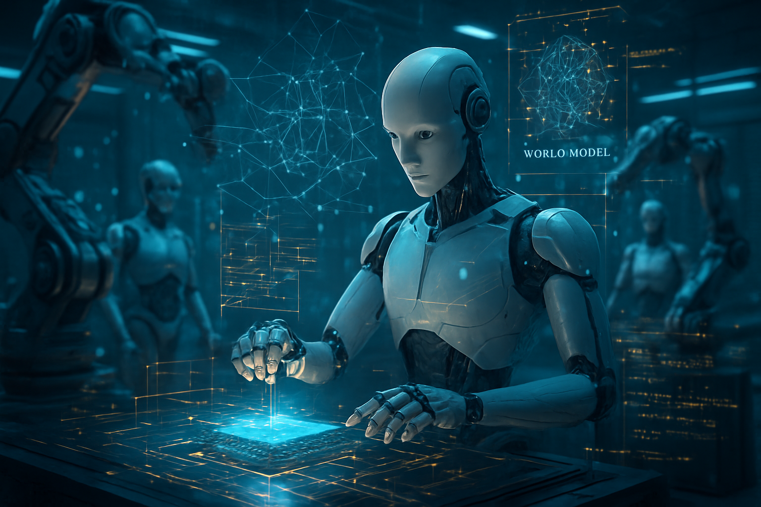
January 14, 2026 — The software development landscape has undergone a tectonic shift over the last 24 months, moving rapidly from simple code completion to full-scale autonomous engineering. What began as "Copilots" that suggested the next line of code has evolved into a sophisticated ecosystem of AI agents capable of navigating complex codebases, managing terminal environments, and resolving high-level tickets with minimal human intervention. This transition, often referred to as the shift from "auto-complete" to "auto-engineer," is fundamentally altering how software is built, maintained, and scaled in the enterprise.
At the heart of this revolution are tools like Cursor and Devin, which have transcended their status as mere plugins to become central hubs of productivity. These platforms no longer just assist; they take agency. Whether it is Anysphere’s Cursor achieving record-breaking adoption or Cognition’s Devin 2.0 operating as a virtual teammate, the industry is witnessing the birth of "vibe coding"—a paradigm where developers focus on high-level architectural intent and system "vibes" while AI agents handle the grueling minutiae of implementation and debugging.
From Suggestions to Solutions: The Technical Leap to Agency
The technical advancements powering today’s AI engineers are rooted in three major breakthroughs: agentic planning, dynamic context discovery, and tool-use mastery. Early iterations of AI coding tools relied on "brute force" long-context windows that often suffered from information overload. However, as of early 2026, tools like Cursor (developed by Anysphere) have implemented Dynamic Context Discovery. This system intelligently fetches only the relevant segments of a repository and external documentation, reducing token waste by nearly 50% while increasing the accuracy of multi-file edits. In Cursor’s "Composer Mode," developers can now describe a complex feature—such as integrating a new payment gateway—and the AI will simultaneously modify dozens of files, from backend schemas to frontend UI components.
The benchmarks for these capabilities have reached unprecedented heights. On the SWE-Bench Verified leaderboard—a human-vetted subset of real-world GitHub issues—the top-performing models have finally broken the 80% resolution barrier. Specifically, Claude 4.5 Opus and GPT-5.2 Codex have achieved scores of 80.9% and 80.0%, respectively. This is a staggering leap from late 2024, when the best agents struggled to clear 20%. These agents are no longer just guessing; they are iterating. They use "computer use" capabilities to open browsers, read documentation for obscure APIs, execute terminal commands, and interpret error logs to self-correct their logic before the human engineer even sees the first draft.
However, the "realism gap" remains a topic of intense discussion. While performance on verified benchmarks is high, the introduction of SWE-Bench Pro—which utilizes private, messy, and legacy-heavy repositories—shows that AI agents still face significant hurdles. Resolution rates on "Pro" benchmarks currently hover around 25%, highlighting that while AI can handle modern, well-documented frameworks with ease, the "spaghetti code" of legacy enterprise systems still requires deep human intuition and historical context.
The Trillion-Dollar IDE War: Market Implications and Disruption
The rise of autonomous engineering has triggered a massive realignment among tech giants and specialized startups. Microsoft (NASDAQ: MSFT) remains the heavyweight champion through GitHub Copilot Workspace, which has now integrated "Agent Mode" powered by GPT-5. Microsoft’s strategic advantage lies in its deep integration with the Azure ecosystem and the GitHub CI/CD pipeline, allowing for "Self-Healing CI/CD" where AI agents automatically fix failing builds. Meanwhile, Google (NASDAQ: GOOGL) has entered the fray with "Antigravity," an agent-first IDE designed for orchestrating fleets of AI workers using the Gemini 3 family of models.
The startup scene is equally explosive. Anysphere, the creator of Cursor, reached a staggering $29.3 billion valuation in late 2025 following a strategic investment round led by Nvidia (NASDAQ: NVDA) and Google. Their dominance in the "agentic editor" space has put traditional IDEs like VS Code on notice, as Cursor offers a more seamless integration of chat and code execution. Cognition, the maker of Devin, has pivoted toward the enterprise "virtual teammate" model, boasting a $10.2 billion valuation and a major partnership with Infosys to deploy AI engineering fleets across global consulting projects.
This shift is creating a "winner-takes-most" dynamic in the developer tool market. Startups that fail to integrate agentic workflows are being rapidly commoditized. Even Amazon (NASDAQ: AMZN) has doubled down on its AWS Toolkit, integrating "Amazon Q Developer" to provide specialized agents for cloud architecture optimization. The competitive edge has shifted from who provides the most accurate code snippet to who provides the most reliable autonomous workflow.
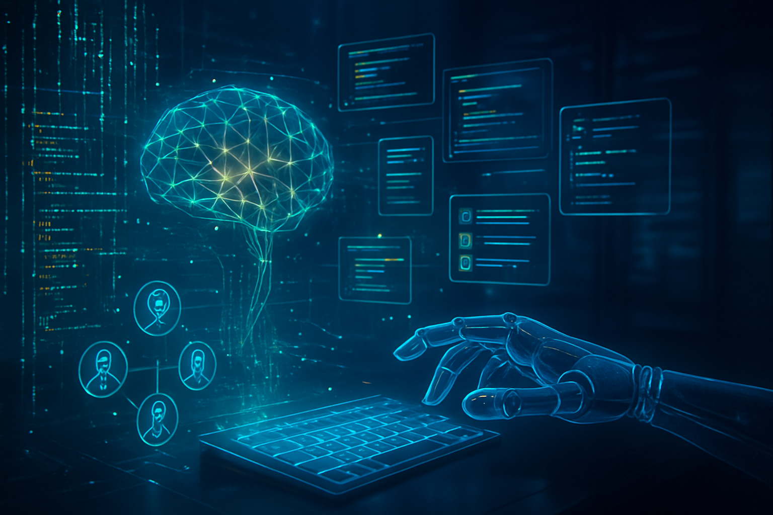
The Architect of Agents: Rethinking the Human Role
As AI moves from a tool to a teammate, the broader significance for the software engineering profession cannot be overstated. We are witnessing the democratization of high-level software creation. Non-technical founders are now using "vibe coding" to build functional MVPs in days that previously took months. However, this has also raised concerns regarding code quality, security, and the future of entry-level engineering roles. While tools like GitHub’s "CVE Remediator" can automatically patch known vulnerabilities, the risk of AI-generated "hallucinated" security flaws remains a persistent threat.
The role of the software engineer is evolving into that of an "Agent Architect." Instead of writing syntax, senior engineers are now spending their time designing system prompts, auditing agentic plans, and managing the orchestration of multiple AI agents working in parallel. This is reminiscent of the shift from assembly language to high-level programming languages; the abstraction layer has simply moved up again. The primary concern among industry experts is "skill atrophy"—the fear that the next generation of developers may lack the fundamental understanding of how systems work if they rely entirely on agents to do the heavy lifting.
Furthermore, the environmental and economic costs of running these massive models are significant. The shift to agentic workflows requires constant, high-compute cycles as agents "think," "test," and "retry" in the background. This has led to a surge in demand for specialized AI silicon, further cementing the market positions of companies like Nvidia (NASDAQ: NVDA) and Advanced Micro Devices (NASDAQ: AMD).
The Road to AGI: What Happens Next?
Looking toward the near future, the next frontier for AI engineering is "Multi-Agent Orchestration." We expect to see systems where a "Manager Agent" coordinates a "UI Agent," a "Database Agent," and a "Security Agent" to build entire applications from a single product requirement document. These systems will likely feature "Long-Term Memory," allowing the AI to remember architectural decisions made months ago, reducing the need for repetitive prompting.
Predicting the next 12 to 18 months, experts suggest that the "SWE-Bench Pro" gap will be the primary target for research. Models that can reason through 20-year-old COBOL or Java monoliths will be the "Holy Grail" for enterprise digital transformation. Additionally, we may see the first "Self-Improving Codebases," where software systems autonomously monitor their own performance metrics and refactor their own source code to optimize for speed and cost without any human trigger.
A New Era of Creation
The transition from AI as a reactive assistant to AI as an autonomous engineer marks one of the most significant milestones in the history of computing. By early 2026, the question is no longer whether AI can write code, but how many AI agents a single human can effectively manage. The benchmarks prove that for modern development, the AI has arrived; the focus now shifts to the reliability of these agents in the chaotic, real-world environments of legacy enterprise software.
As we move forward, the success of companies will be defined by their "agentic density"—the ratio of AI agents to human engineers and their ability to harness this new workforce effectively. While the fear of displacement remains, the immediate reality is a massive explosion in human creativity, as the barriers between an idea and a functioning application continue to crumble.
This content is intended for informational purposes only and represents analysis of current AI developments.
TokenRing AI delivers enterprise-grade solutions for multi-agent AI workflow orchestration, AI-powered development tools, and seamless remote collaboration platforms.
For more information, visit https://www.tokenring.ai/.