As of February 6, 2026, the global technology sector is grappling with a supply chain crisis of historic proportions. What industry analysts have dubbed the "Memory Famine" or "RAMpocalypse" has officially reached a boiling point, as a new report from TrendForce confirms that the insatiable demand for Artificial Intelligence infrastructure has effectively stripped the world of its conventional memory supply. This structural imbalance is no longer a localized issue for server farms; it has spilled over into the consumer market, threatening to double the price of PCs and smartphones in a single quarter.
The immediate significance of this event cannot be overstated. For the first time in the history of the semiconductor industry, the production of high-performance AI chips is directly cannibalizing the manufacturing capacity required for everyday electronics. As Tier-1 manufacturers scramble to secure remaining inventory, the "RAMpocalypse" marks a fundamental shift where memory is no longer treated as a ubiquitous commodity, but as a scarce strategic asset reserved for the highest bidder.
The Technical Reality: Why the Numbers are Skyrocketing
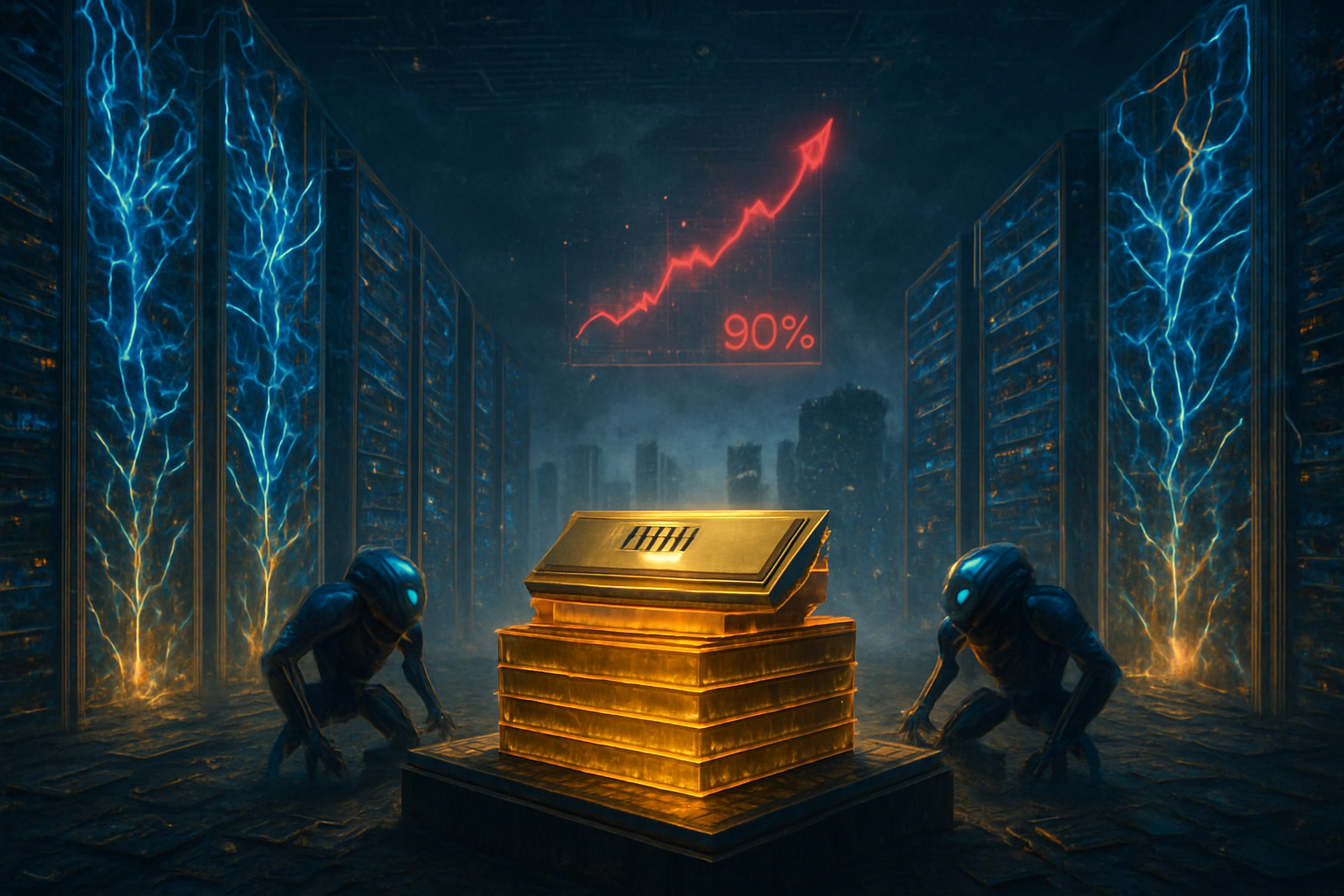
The updated forecast from TrendForce has sent shockwaves through the industry. Initially, analysts predicted a significant but manageable rise in component costs for early 2026. However, the revised data indicates that DRAM (Dynamic Random Access Memory) contract prices will surge by a staggering 90-95% in Q1 2026 alone. PC DRAM is particularly vulnerable, with some high-performance DDR5 modules expected to see price hikes exceeding 110% as manufacturers prioritize more lucrative server-grade components.
The crisis is equally severe in the storage sector. NAND Flash prices, essential for the Solid State Drives (SSDs) found in everything from laptops to data centers, are projected to rise by 55-60% this quarter. The technical driver behind this surge is the massive reallocation of wafer capacity. Major chipmakers like Samsung Electronics (KRX: 005930), SK Hynix (KRX: 000660), and Micron Technology (NASDAQ: MU) have pivoted their production lines to High Bandwidth Memory (HBM3E and HBM4). These advanced stacks are critical for powering the latest AI GPUs from companies like Nvidia (NASDAQ: NVDA), but they require three times the wafer capacity per bit compared to standard consumer RAM.
This "wafer war" means that for every HBM module produced for an AI supercomputer, the industry loses the capacity to manufacture multiple sticks of consumer DDR5. This differs from previous supply shortages, which were often caused by factory fires or temporary logistics bottlenecks. The 2026 Famine is a deliberate, structural pivot by manufacturers toward the high-margin AI sector, leaving the consumer research community and industry experts alarmed by the rapid "spec regression" appearing in new hardware. Budget laptops that were standardizing on 16GB of RAM just a year ago are now being redesigned with 8GB or even 4GB to keep retail prices from doubling.
Corporate Warfare: Hoarding and the Great Data Center Land Grab
The primary architects of this shortage are the world’s largest Cloud Service Providers (CSPs). Tech giants including Microsoft (NASDAQ: MSFT), Alphabet (NASDAQ: GOOGL), Meta Platforms (NASDAQ: META), and Amazon (NASDAQ: AMZN) have entered a phase of "strategic hoarding." By utilizing their massive cash reserves, these companies have signed multi-year Long-Term Agreements (LTAs) that effectively lock in up to 70% of the world’s memory production through 2027.
This aggressive procurement strategy has left traditional hardware OEMs (Original Equipment Manufacturers) in a precarious position. Companies like Dell Technologies (NYSE: DELL) and HP Inc. (NYSE: HPQ) are reportedly engaged in bidding wars with smartphone makers like Apple (NASDAQ: AAPL) just to secure the components necessary for their 2026 product lineups. For the first time, memory has overtaken processors as the single most expensive component in the Bill of Materials (BOM) for a standard laptop, now accounting for nearly 30% of the total manufacturing cost.
While the memory manufacturers themselves—Samsung, SK Hynix, and Micron—are seeing record-breaking profit margins, the broader tech ecosystem is reeling. Smaller hardware startups and second-tier PC brands are being priced out of the market entirely. The competitive advantage has shifted decisively toward those who own their own silicon or have the deepest pockets to pre-pay for years of supply, further consolidating power within the "Magnificent Seven" and a handful of semiconductor titans.
Beyond the Desktop: The Global Implications of the Famine
The "RAMpocalypse" is not confined to the halls of Silicon Valley; its ripples are being felt across the entire global economy. This crisis represents a "permanent reallocation" of technological resources. In the same way the 2021 chip shortage slowed the automotive industry, the 2026 Memory Famine is now causing production delays for smart appliances, televisions, and automobiles. As manufacturers rush to upgrade their fabrication plants to handle advanced AI memory, they are abandoning the "legacy" nodes that produce cheaper, simpler chips for everyday devices.
Comparisons are already being drawn to the 1970s oil crisis, where a single vital resource became the bottleneck for global productivity. The AI landscape is now the dominant engine of the world economy, and its hunger for memory is so vast that it is effectively starving other sectors. Tech ethicists and market analysts are raising concerns about a widening "digital divide," where only the wealthiest institutions can afford the hardware necessary to run modern, AI-enhanced software, while average consumers are stuck with increasingly obsolete or overpriced hardware.
Furthermore, this event highlights the fragility of a global supply chain that has become overly dependent on a few specific geographic hubs and manufacturers. The transition of memory from a consumer commodity to an industrial necessity marks a milestone in the AI era, signaling that the "gold rush" for computing power has reached a point of physical limitation.
The Road Ahead: Fabs, Efficiency, and a Precarious Future
Industry experts predict that relief is unlikely to arrive before late 2027 or early 2028. While companies like Micron and Samsung are breaking ground on massive new "mega-fabs" in the United States and South Korea, these facilities take years to reach full production capacity. In the near term, the focus is shifting toward "AI efficiency"—developing software and models that require less memory to operate. However, as long as the arms race for Large Language Models (LLMs) and generative video continues, the pressure on the memory market will remain intense.
On the horizon, we may see the emergence of new memory architectures designed to bridge the gap between high-cost HBM and low-cost DDR5. Applications in edge computing and "AI on device" will likely drive innovation in more efficient LPDDR6 standards, but these are currently in the early stages of testing. For now, the "RAMpocalypse" forces a period of austerity on the consumer market, where users are encouraged to repair and maintain their current devices rather than upgrading.
A Summary of the Memory Crisis
The 2026 Memory Famine is a watershed moment for the technology industry. It serves as a stark reminder that even the most advanced software is ultimately tethered to physical silicon and wafers. The key takeaways are clear: DRAM and NAND prices are hitting historic highs, AI data centers have become the primary consumers of global hardware, and the consumer electronics market is facing a period of significant inflation and specification stagnation.
As we move through the first quarter of 2026, the industry will be watching for any signs of production breakthroughs or shifts in AI training methods that could reduce the demand for memory. For now, the "RAMpocalypse" remains the defining economic story of the year, fundamentally altering how we value, purchase, and utilize technology in an AI-first world.
This content is intended for informational purposes only and represents analysis of current AI developments.
TokenRing AI delivers enterprise-grade solutions for multi-agent AI workflow orchestration, AI-powered development tools, and seamless remote collaboration platforms.
For more information, visit https://www.tokenring.ai/.