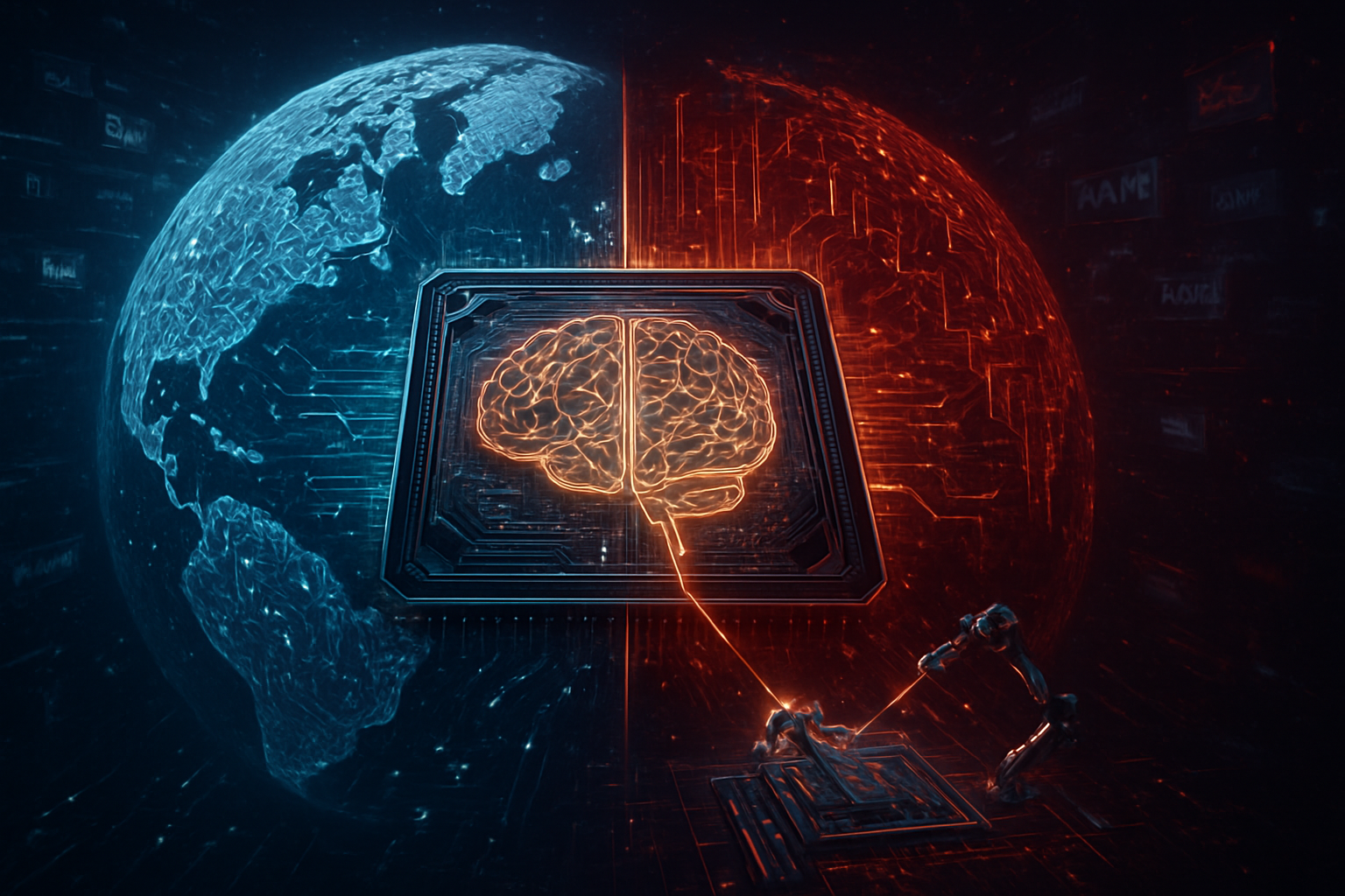
As of January 13, 2026, the global semiconductor landscape has undergone a radical transformation, evolving from a unified global market into a strictly bifurcated "Silicon Curtain." The start of the new year has been marked by the implementation of the Remote Access Security Act, a landmark piece of U.S. legislation that effectively closed the "cloud loophole," preventing Chinese entities from accessing high-end compute power via offshore data centers. This move, combined with the fragile "Busan Truce" of late 2025, has solidified a new era of technological mercantilism where data, design, and hardware are treated as the ultimate sovereign assets.
The immediate significance of these developments cannot be overstated. For the first time in the history of the digital age, the two largest economies in the world are operating on fundamentally different hardware roadmaps. While the U.S. and its allies have consolidated around a regulated "AI Diffusion Rule," China has accelerated its "Big Fund III" investments, shifting from mere chip manufacturing to solving critical chokepoints in lithography and advanced 3D packaging. This geopolitical friction is no longer just a trade dispute; it is an existential race for computational supremacy that will define the next decade of artificial intelligence development.
The technical architecture of this divide is most visible in the divergence between NVIDIA (NVDA:NASDAQ) and its domestic Chinese rivals. Following the 2025 AI Diffusion Rule, the U.S. government established a rigorous three-tier export system. While top-tier allies enjoy unrestricted access to the latest Blackwell and Rubin architectures, Tier 3 nations like China are restricted to severely nerfed versions of high-end hardware. To maintain a foothold in the massive Chinese market, NVIDIA recently began navigating a complex "25% Revenue-Sharing Fee" protocol, allowing the export of the H200 to China only if a quarter of the revenue is redirected to the U.S. Treasury to fund domestic R&D—a move that has sparked intense debate among industry analysts regarding corporate sovereignty.
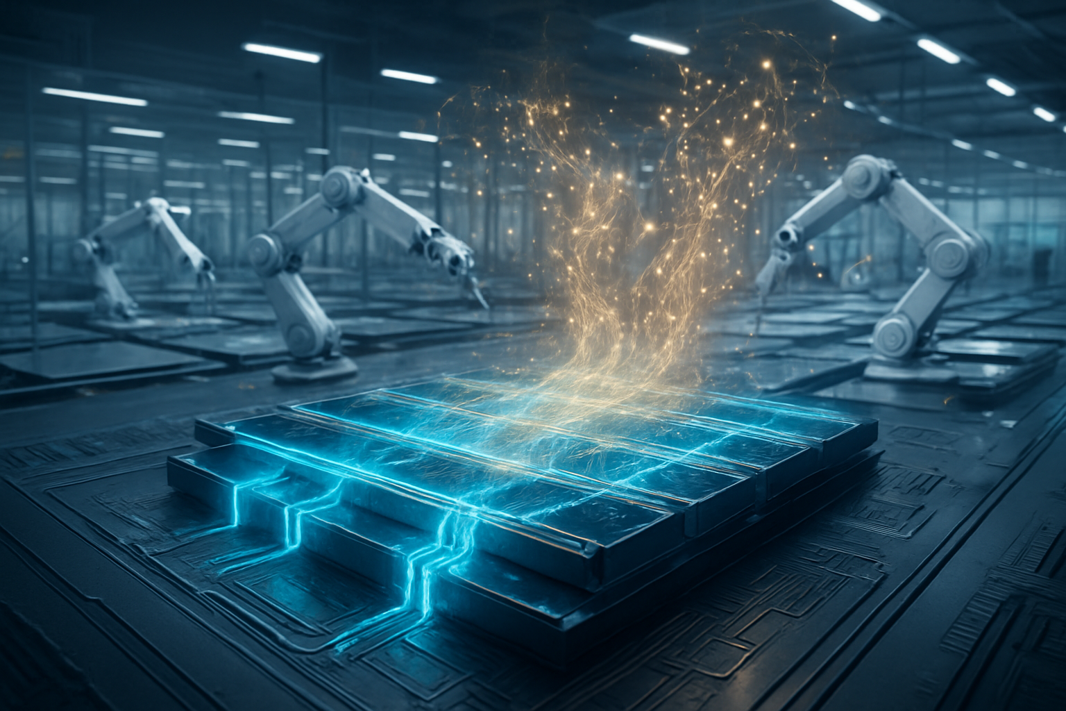
Technically, the race has shifted from single-chip performance to "system-level" scaling. Because Chinese firms like Huawei are largely restricted from the 3nm and 2nm nodes produced by TSMC (TSM:NYSE), they have pivoted to innovative interconnect technologies. In late 2025, Huawei introduced UnifiedBus 2.0, a proprietary protocol that allows for the clustering of up to one million lower-performance 7nm chips into massive "SuperClusters." This approach argues that raw quantity and high-bandwidth connectivity can compensate for the lack of cutting-edge transistor density. Initial reactions from the AI research community suggest that while these clusters are less energy-efficient, they are proving surprisingly capable of training large language models (LLMs) that rival Western counterparts in specific benchmarks.
Furthermore, China’s Big Fund III, fueled by approximately $48 billion in capital, has successfully localized several key components of the supply chain. Companies such as Piotech Jianke have made breakthroughs in hybrid bonding and 3D integration, allowing China to bypass some of the limitations imposed by the lack of ASML (ASML:NASDAQ) Extreme Ultraviolet (EUV) lithography machines. The focus is no longer on matching the West's 2nm roadmap but on perfecting "advanced packaging" to squeeze maximum performance out of existing 7nm and 5nm capabilities. This "chokepoint-first" strategy marks a significant departure from previous years, where the focus was simply on expanding mature node capacity.
The implications for tech giants and startups are profound, creating clear winners and losers in this fragmented market. Intel (INTC:NASDAQ) has emerged as a central pillar of the U.S. strategy, with the government taking a historic 10% equity stake in the company in August 2025 to ensure the "Secure Enclave" program—intended for military-grade chip production—remains on American soil. This move has bolstered Intel's position as a national champion, though it has faced criticism for potential market distortions. Meanwhile, TSMC continues to navigate a delicate balance, ramping up its "GIGAFAB" cluster in Arizona, which is expected to begin trial runs for domestic AI packaging by mid-2026.
In the private sector, the competitive landscape has been disrupted by the rise of "Sovereign AI." Major Chinese firms like Alibaba and Tencent have been privately directed by Beijing to prioritize Huawei’s Ascend 910C and the upcoming 910D chips over NVIDIA’s China-specific H20 models. This has forced a major market positioning shift for NVIDIA, which now relies more heavily on demand from the Middle East and Southeast Asia to offset the tightening Chinese restrictions. For startups, the divide is even more stark; Western AI startups benefit from a surplus of compute in "Tier 1" regions, while those in "Tier 3" regions are forced to optimize their algorithms for "compute-constrained" environments, potentially leading to more efficient software architectures in the East.
The disruption extends to the supply of critical materials. Although the "Busan Truce" of November 2025 saw China temporarily suspend its export bans on gallium, germanium, and antimony, U.S. companies have used this reprieve to aggressively diversify their supply chains. Samsung Electronics (005930:KRX) has capitalized on this volatility by accelerating its $17 billion fab in Taylor, Texas, positioning itself as a primary alternative to TSMC for U.S.-based companies looking to mitigate geopolitical risk. The net result is a market where strategic resilience is now valued as highly as technical performance, fundamentally altering the ROI calculations for the world's largest tech investors.
This shift toward semiconductor self-sufficiency represents a broader trend of "technological decoupling" that hasn't been seen since the Cold War. In the previous era of AI breakthroughs, such as the 2012 ImageNet moment or the 2017 Transformer paper, progress was driven by global collaboration and an open exchange of ideas. Today, the hardware required to run these models has become a "dual-use" asset, as vital to national security as enriched uranium. The creation of the "Silicon Curtain" means that the AI landscape is now inextricably tied to geography, with the "compute-rich" and the "compute-poor" increasingly defined by their alliance structures.
The potential concerns are twofold: a slowdown in global innovation and the risk of "black box" development. With China and the U.S. operating in siloed ecosystems, there is a diminishing ability for international oversight on AI safety and ethics. Comparison to previous milestones, such as the 1990s semiconductor boom, shows a complete reversal in philosophy; where the industry once sought the lowest-cost manufacturing regardless of location, it now accepts significantly higher costs in exchange for "friend-shoring" and supply chain transparency. This shift has led to higher prices for consumer electronics but has stabilized the strategic outlook for Western defense sectors.
Furthermore, the emergence of the "Remote Access Security Act" in early 2026 marks the end of the cloud as a neutral territory. For years, the cloud allowed for a degree of "technological arbitrage," where firms could bypass local hardware restrictions by renting GPUs elsewhere. By closing this loophole, the U.S. has effectively asserted that compute power is a physical resource that cannot be abstracted away from its national origin. This sets a significant precedent for future digital assets, including cryptographic keys and large-scale datasets, which may soon face similar geographic restrictions.
Looking ahead to the remainder of 2026 and beyond, the industry is bracing for the Q2 release of Huawei’s Ascend 910D, which is rumored to match the performance of the NVIDIA H100 through sheer massive-scale interconnectivity. The near-term focus for the U.S. will be the continued implementation of the CHIPS Act, with Micron (MU:NASDAQ) expected to begin production of high-bandwidth memory (HBM) wafers at its new Boise facility by 2027. The long-term challenge remains the "1nm roadmap," where the physical limits of silicon will require even deeper collaboration between the few remaining players capable of such engineering—namely TSMC, Intel, and Samsung.
Experts predict that the next frontier of this conflict will move into silicon photonics and quantum-resistant encryption. As traditional transistor scaling reaches its plateau, the ability to move data using light instead of electricity will become the new technical battleground. Additionally, there is a looming concern regarding the "2027 Cliff," when the temporary mineral de-escalation from the Busan Truce is set to expire. If a permanent agreement is not reached by then, the global semiconductor industry could face a catastrophic shortage of the rare earth elements required for advanced chip manufacturing.
The key takeaway from the current geopolitical climate is that the semiconductor industry is no longer governed solely by Moore's Law, but by the laws of national security. The era of the "global chip" is over, replaced by a dual-track system that prioritizes domestic self-sufficiency and strategic alliances. While this has spurred massive investment and a "renaissance" of Western manufacturing, it has also introduced a layer of complexity and cost that will be felt across every sector of the global economy.
In the history of AI, 2025 and early 2026 will be remembered as the years when the "Silicon Curtain" was drawn. The long-term impact will be a divergence in how AI is trained, deployed, and regulated, with the West focusing on high-density, high-efficiency models and the East pioneering massive-scale, distributed "SuperClusters." In the coming weeks and months, the industry will be watching for the first "Post-Cloud" AI breakthroughs and the potential for a new round of mineral export restrictions that could once again tip the balance of power in the world’s most important technology sector.
This content is intended for informational purposes only and represents analysis of current AI developments.
TokenRing AI delivers enterprise-grade solutions for multi-agent AI workflow orchestration, AI-powered development tools, and seamless remote collaboration platforms.
For more information, visit https://www.tokenring.ai/.