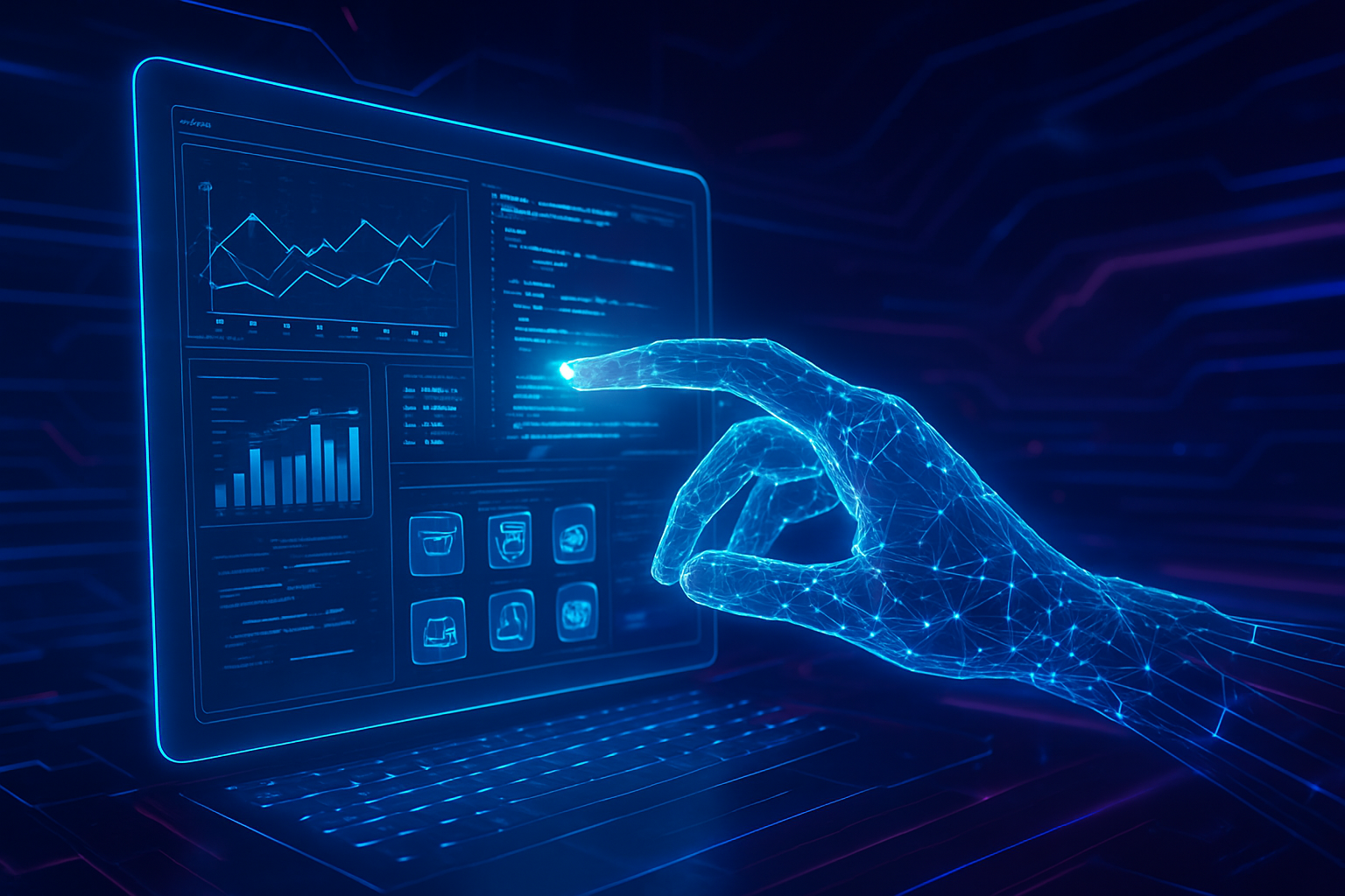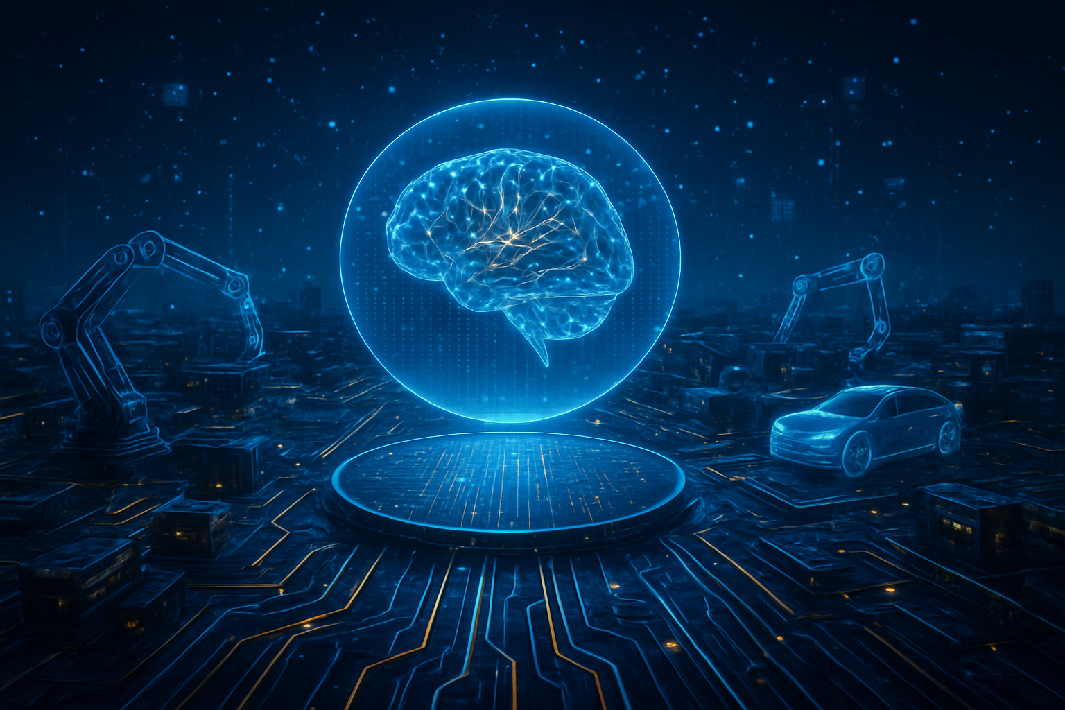
For years, the narrative of artificial intelligence was defined by "bigger is better." Massive, power-hungry models like GPT-4 required sprawling data centers and billion-dollar investments to function. However, as of early 2026, the tide has officially turned. The "Small Model Revolution"—a movement toward highly efficient Small Language Models (SLMs) like Meta’s Llama 3.2 1B and 3B—has successfully migrated world-class intelligence from the cloud directly into the silicon of our smartphones. This shift marks a fundamental change in how we interact with technology, moving away from centralized, latency-heavy APIs toward instant, private, and local digital assistants.
The significance of this transition cannot be overstated. By January 2026, the industry has reached an "Inference Inflection Point," where the majority of daily AI tasks—summarizing emails, drafting documents, and even complex coding—are handled entirely on-device. This development has effectively dismantled the "Cloud Tax," the high operational costs and privacy risks associated with sending personal data to remote servers. What began as a technical experiment in model compression has matured into a sophisticated ecosystem where your phone is no longer just a portal to an AI; it is the AI.
The Architecture of Efficiency: How SLMs Outperform Their Weight Class
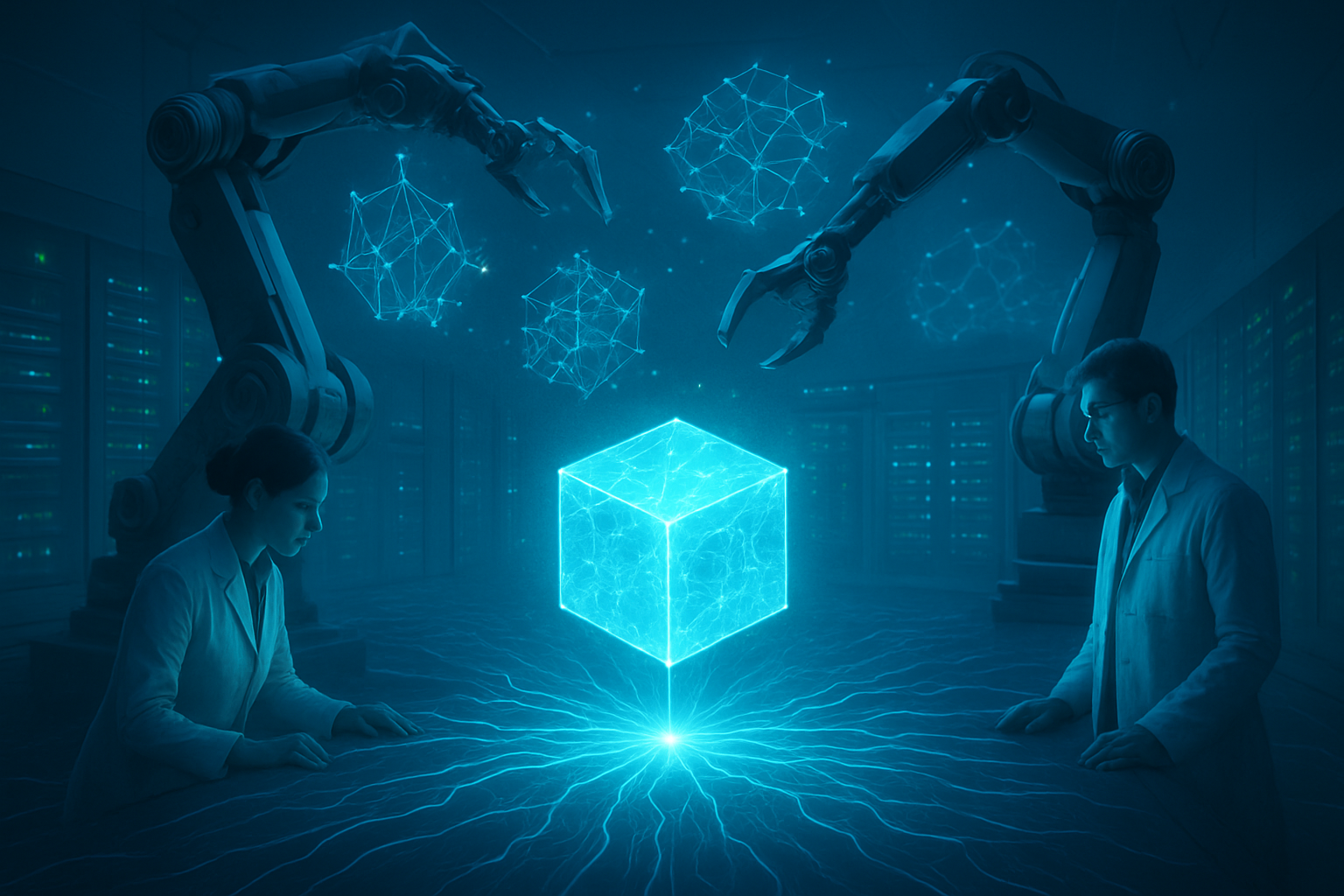
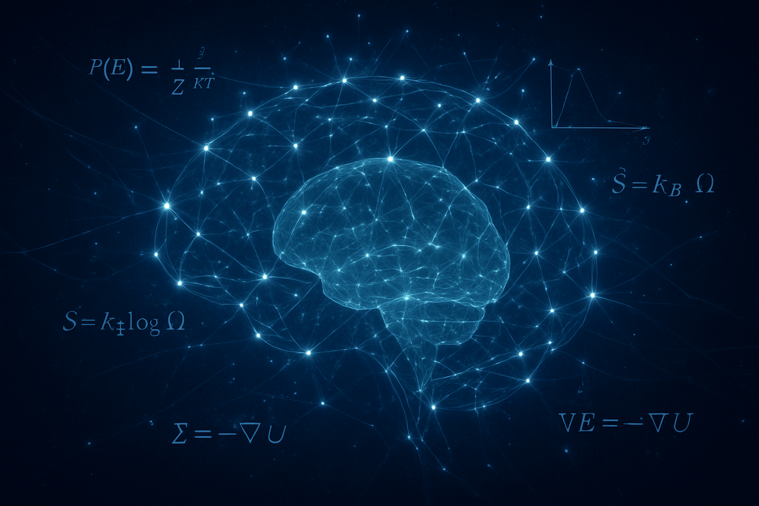
The technical breakthrough that enabled this revolution lies in the transition from training models from scratch to "knowledge distillation" and "structured pruning." When Meta Platforms Inc. (NASDAQ: META) released Llama 3.2 in late 2024, it demonstrated that a 3-billion parameter model could achieve reasoning capabilities that previously required 10 to 20 times the parameters. Engineers achieved this by using larger "teacher" models to train smaller "students," effectively condensing the logic and world knowledge of a massive LLM into a compact footprint. These models feature a massive 128K token context window, allowing them to process entire books or long legal documents locally on a mobile device without running out of memory.
This software efficiency is matched by unprecedented hardware synergy. The latest mobile chipsets, such as the Qualcomm Inc. (NASDAQ: QCOM) Snapdragon 8 Elite and the Apple Inc. (NASDAQ: AAPL) A19 Pro, are specifically designed with dedicated Neural Processing Units (NPUs) to handle these workloads. By early 2026, these chips deliver over 80 Tera Operations Per Second (TOPS), allowing a model like Llama 3.2 1B to run at speeds exceeding 30 tokens per second. This is faster than the average human reading speed, making the AI feel like a seamless extension of the user’s own thought process rather than a slow, typing chatbot.
Furthermore, the integration of Grouped-Query Attention (GQA) has solved the memory bandwidth bottleneck that previously plagued mobile AI. By reducing the amount of data the processor needs to fetch from the phone’s RAM, SLMs can maintain high performance while consuming significantly less battery. Initial reactions from the research community have shifted from skepticism about "small model reasoning" to a race for "ternary" efficiency. We are now seeing the emergence of 1.58-bit models—often called "BitNet" architectures—which replace complex multiplications with simple additions, potentially reducing AI energy footprints by another 70% in the coming year.
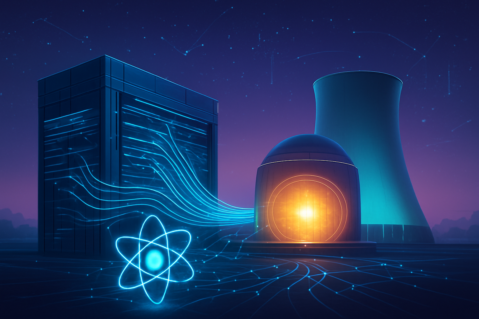
The Silicon Power Play: Tech Giants Battle for the Edge
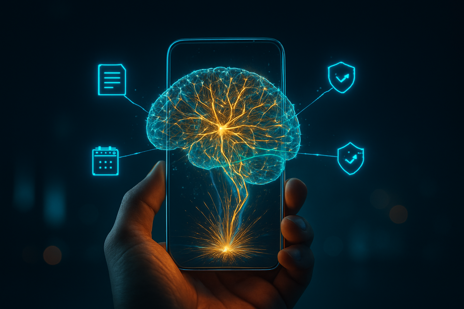
The shift to local processing has ignited a strategic war among tech giants, as the control of AI moves from the data center to the device. Apple has leveraged its vertical integration to position "Apple Intelligence" as a privacy-first moat, ensuring that sensitive user data never leaves the iPhone. By early 2026, the revamped Siri, powered by specialized on-device foundation models, has become the primary interface for millions, performing multi-step tasks like "Find the receipt from my dinner last night and add it to my expense report" without ever touching the cloud.
Meanwhile, Microsoft Corporation (NASDAQ: MSFT) has pivoted its Phi model series to target the enterprise sector. Models like Phi-4 Mini have achieved reasoning parity with the original GPT-4, allowing businesses to deploy "Agentic OS" environments on local laptops. This has been a massive disruption for cloud-only providers; enterprises in regulated industries like healthcare and finance are moving away from expensive API subscriptions in favor of self-hosted SLMs. Alphabet Inc. (NASDAQ: GOOGL) has responded with its Gemma 3 series, which is natively multimodal, allowing Android devices to process text, image, and video inputs simultaneously on a single chip.
The competitive landscape is no longer just about who has the largest model, but who has the most efficient one. This has created a "trickle-down" effect where startups can now build powerful AI applications without the massive overhead of cloud computing costs. Market data from late 2025 indicates that the cost to achieve high-level AI performance has plummeted by over 98%, leading to a surge in specialized "Edge AI" startups that focus on everything from real-time translation to autonomous local coding assistants.
The Privacy Paradigm and the End of the Cloud Tax
The wider significance of the Small Model Revolution is rooted in digital sovereignty. For the first time since the rise of the cloud, users have regained control over their data. Because SLMs process information locally, they are inherently immune to the data breaches and privacy concerns that have dogged centralized AI. This is particularly critical in the wake of the EU AI Act, which reached full compliance requirements in 2026. Local processing allows companies to satisfy strict GDPR and HIPAA requirements by ensuring that patient records or proprietary trade secrets remain behind the corporate firewall.
Beyond privacy, the "democratization of intelligence" is a key social impact. In regions with limited internet connectivity, on-device AI provides a "pocket brain" that works in airplane mode. This has profound implications for education and emergency services in developing nations, where access to high-speed data is not guaranteed. The move to SLMs has also mitigated the "Cloud Tax"—the recurring monthly fees that were becoming a barrier to AI adoption for small businesses. By moving inference to the user's hardware, the marginal cost of an AI query has effectively dropped to zero.
However, this transition is not without concerns. The rise of powerful, uncensored local models has sparked debates about AI safety and the potential for misuse. Unlike cloud models, which can be "turned off" or filtered by the provider, a model running locally on a phone is much harder to regulate. This has led to a new focus on "on-device guardrails"—lightweight safety layers that run alongside the SLM to prevent the generation of harmful content while respecting the user's privacy.
Beyond Chatbots: The Rise of the Autonomous Agent
Looking toward the remainder of 2026 and into 2027, the focus is shifting from "chatting" to "acting." The next generation of SLMs, such as the rumored Llama 4 "Scout" series, are being designed as autonomous agents with "screen awareness." These models will be able to "see" what is on a user's screen and navigate apps just like a human would. This will transform smartphones from passive tools into proactive assistants that can book travel, manage calendars, and coordinate complex projects across multiple platforms without manual intervention.
Another major frontier is the integration of 6G edge computing. While the models themselves run locally, 6G will allow for "split-inference," where a mobile device handles the privacy-sensitive parts of a task and offloads the most compute-heavy reasoning to a nearby edge server. This hybrid approach promises to deliver the power of a trillion-parameter model with the latency of a local one. Experts predict that by 2028, the distinction between "local" and "cloud" AI will have blurred entirely, replaced by a fluid "Intelligence Fabric" that scales based on the task at hand.
Conclusion: A New Era of Personal Computing
The Small Model Revolution represents one of the most significant milestones in the history of artificial intelligence. It marks the transition of AI from a distant, mysterious power housed in massive server farms to a personal, private, and ubiquitous utility. The success of models like Llama 3.2 1B and 3B has proven that intelligence is not a function of size alone, but of architectural elegance and hardware optimization.
As we move further into 2026, the key takeaway is that the "AI in your pocket" is no longer a toy—it is a sophisticated tool capable of handling the majority of human-AI interactions. The long-term impact will be a more resilient, private, and cost-effective digital world. In the coming weeks, watch for major announcements at the upcoming spring hardware summits, where the next generation of "Ternary" chips and "Agentic" operating systems are expected to push the boundaries of what a handheld device can achieve even further.
This content is intended for informational purposes only and represents analysis of current AI developments.
TokenRing AI delivers enterprise-grade solutions for multi-agent AI workflow orchestration, AI-powered development tools, and seamless remote collaboration platforms.
For more information, visit https://www.tokenring.ai/.