Tag: AI

  • Silicon Sovereignty: 2026 Marks the Dawn of the American Semiconductor Renaissance

    Silicon Sovereignty: 2026 Marks the Dawn of the American Semiconductor Renaissance

    The year 2026 has arrived as a definitive watershed moment for the global technology landscape, marking the transition of "Silicon Sovereignty" from a policy ambition to a physical reality. As of January 5, 2026, the United States has successfully re-shored a critical mass of advanced logic manufacturing, effectively ending a decades-long reliance on concentrated Asian supply chains. This shift is headlined by the commencement of high-volume manufacturing at Intel's state-of-the-art facilities in Arizona and the stabilization of TSMC’s domestic operations, signaling a new era where the world's most advanced AI hardware is once again "Made in America."

    The immediate significance of these developments cannot be overstated. For the first time in the modern era, the U.S. domestic supply chain is capable of producing sub-5nm chips at scale, providing a vital "Silicon Shield" against geopolitical volatility in the Taiwan Strait. While the road has been marred by strategic delays in the Midwest and shifting federal priorities, the operational status of the Southwest's "Silicon Desert" hubs confirms that the $52 billion bet placed by the CHIPS and Science Act is finally yielding its high-tech dividends.

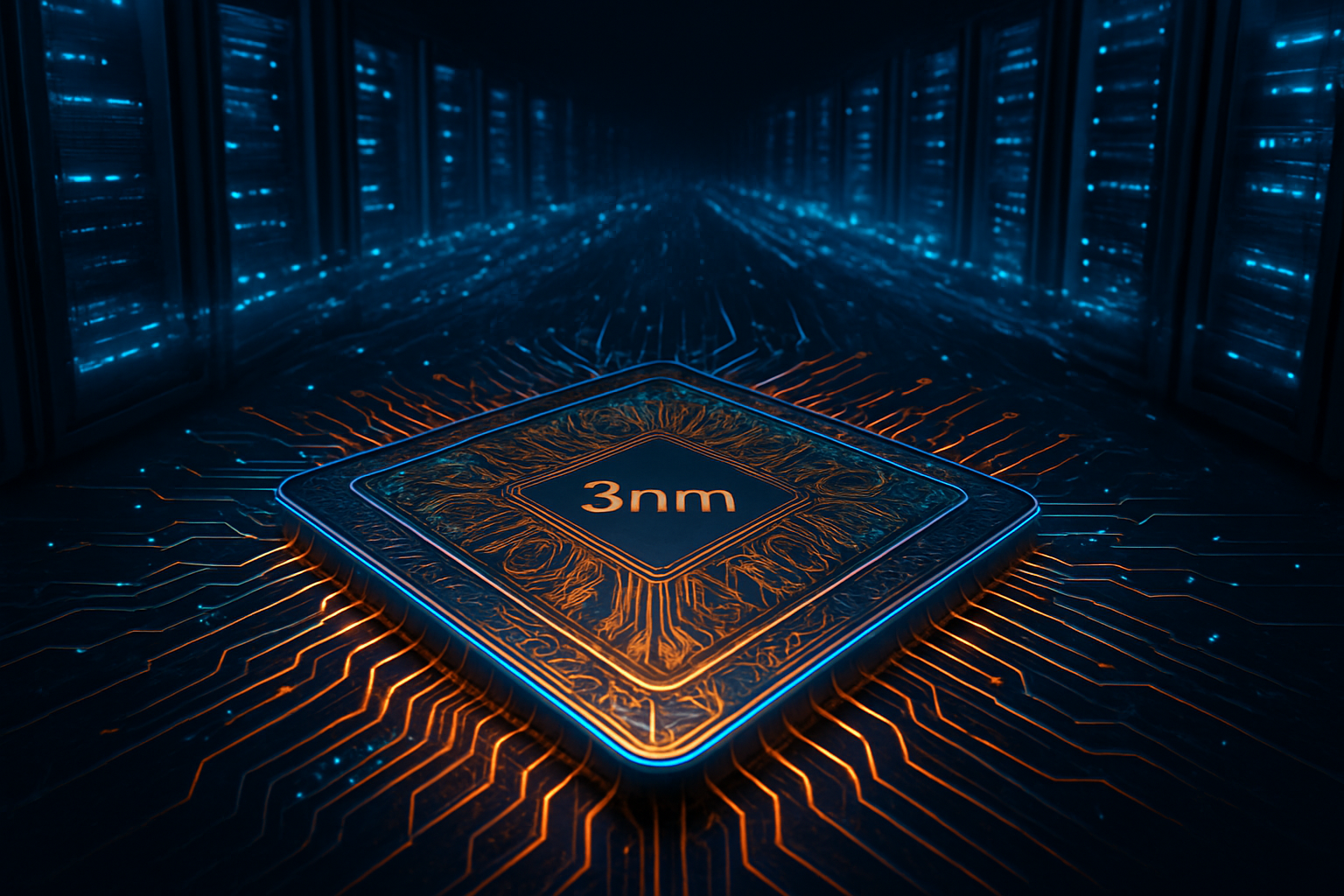
    The Arizona Vanguard: 1.8nm and 4nm Realities

    The centerpiece of this manufacturing resurgence is Intel (NASDAQ: INTC) and its Fab 52 at the Ocotillo campus in Chandler, Arizona. As of early 2026, Fab 52 has officially transitioned into High-Volume Manufacturing (HVM) using the company’s ambitious 18A (1.8nm-class) process node. This technical achievement marks the first time a U.S.-based facility has surpassed the 2nm threshold, successfully integrating revolutionary RibbonFET gate-all-around transistors and PowerVia backside power delivery. Intel’s 18A node is currently powering the next generation of Panther Lake AI PC processors and Clearwater Forest server CPUs, with the fab ramping toward a target capacity of 40,000 wafer starts per month.

    Simultaneously, TSMC (NYSE: TSM) has silenced skeptics with the performance of its first Arizona facility, Fab 21. Initially plagued by labor disputes and cultural friction, the fab reached a staggering 92% yield rate for its 4nm (N4) process by the end of 2025—surpassing the yields of its comparable "mother fabs" in Taiwan. This operational efficiency has allowed TSMC to fulfill massive domestic orders for Apple (NASDAQ: AAPL) and Nvidia (NASDAQ: NVDA), ensuring that the silicon driving the world’s most advanced AI models and consumer devices is forged on American soil.

    However, the "Silicon Heartland" narrative has faced a reality check in the Midwest. Intel’s massive "Ohio One" complex in New Albany has seen its production timeline pushed back significantly. Originally slated for a 2025 opening, the facility is now expected to reach high-volume production no earlier than 2030. Intel has characterized this as a "strategic slowing" to align capital expenditures with a softening data center market and to navigate the transition to the "One Big Beautiful Bill Act" (OBBBA) of 2025, which restructured federal semiconductor incentives. Despite the delay, the Ohio site remains a cornerstone of the long-term U.S. strategy, currently serving as a massive shell project that represents a $28 billion commitment to future-proofing the domestic industry.

    Market Dynamics and the New Competitive Moat

    The successful ramp-up of domestic fabs has fundamentally altered the strategic positioning of the world’s largest tech giants. Companies like Nvidia and Apple, which previously faced "single-source" risks tied to Taiwan’s geopolitical status, now possess a diversified manufacturing base. This domestic capacity acts as a competitive moat, insulating these firms from potential export disruptions and the "Silicon Curtain" that has increasingly bifurcated the global market into Western and Eastern technological blocs.

    For Intel, the 2026 milestone is a make-or-break moment for its foundry services. By delivering 18A on schedule in Arizona, Intel is positioning itself as a viable alternative to TSMC for external customers seeking "sovereign-grade" silicon. Meanwhile, Samsung (KRX: 005930) is preparing to join the fray; its Taylor, Texas facility has pivoted exclusively to 2nm Gate-All-Around (GAA) technology. With mass production in Texas expected by late 2026, Samsung is already securing "anchor" AI clients like Tesla (NASDAQ: TSLA), further intensifying the competition for domestic manufacturing dominance.

    This re-shoring effort has also disrupted the traditional cost structures of the industry. Under the new policy frameworks of 2025 and 2026, "trusted" domestic silicon commands a market premium. The introduction of calibrated tariffs—including a 100% duty on Chinese-made semiconductors—has effectively neutralized the price advantage of overseas manufacturing for the U.S. market. This has forced startups and established AI labs alike to prioritize supply chain resilience over pure margin, leading to a surge in long-term domestic supply agreements.

    Geopolitics and the Silicon Shield

    The broader significance of the 2026 landscape lies in the concept of "Silicon Sovereignty." The U.S. government has moved away from the globalized efficiency models of the early 2000s, treating high-end semiconductors as a controlled strategic asset similar to enriched uranium. This "managed restriction" era is designed to ensure that the U.S. maintains a two-generation lead over adversarial nations. The Arizona and Texas hubs now provide a critical buffer; even in a worst-case scenario involving regional instability in Asia, the U.S. is on track to produce 20% of the world's leading-edge logic chips domestically by the end of the decade.

    This shift has also birthed massive public-private partnerships like "Project Stargate," a $500 billion initiative involving Oracle (NYSE: ORCL) and other major players to build hyper-scale AI data centers directly adjacent to these new power and manufacturing hubs. The first Stargate campus in Abilene, Texas, exemplifies the new American industrial model: a vertically integrated ecosystem where energy, silicon, and intelligence are co-located to minimize latency and maximize security.

    However, concerns remain regarding the "Silicon Curtain" and its impact on global innovation. The bifurcation of the market has led to redundant R&D costs and a fragmented standards environment. Critics argue that while the U.S. has secured its own supply, the resulting trade barriers could slow the overall pace of AI development by limiting the cross-pollination of hardware and software breakthroughs between East and West.

    The Horizon: 2nm and Beyond

    Looking toward the late 2020s, the focus is already shifting from 1.8nm to the sub-1nm frontier. The success of the Arizona fabs has set the stage for the next phase of the CHIPS Act, which will likely focus on advanced packaging and "glass substrate" technologies—the next bottleneck in AI chip performance. Experts predict that by 2028, the U.S. will not only lead in chip design but also in the complex assembly and testing processes that are currently concentrated in Southeast Asia.

    The next major challenge will be the workforce. While the facilities are now operational, the industry faces a projected shortfall of 50,000 specialized engineers by 2030. Addressing this "talent gap" through expanded immigration pathways for high-tech workers and domestic vocational programs will be the primary focus of the 2027 policy cycle. If the U.S. can solve the labor equation as successfully as it has the infrastructure equation, the "Silicon Heartland" may eventually span from the deserts of Arizona to the plains of Ohio.

    A New Chapter in Industrial History

    As we reflect on the state of the industry in early 2026, the progress is undeniable. The high-volume output at Intel’s Fab 52 and the high yields at TSMC’s Arizona facility represent a historic reversal of the offshoring trends that defined the last forty years. While the delays in Ohio serve as a reminder of the immense difficulty of building these "most complex machines on Earth," the momentum is clearly on the side of domestic manufacturing.

    The significance of this development in AI history is profound. We have moved from the era of "Software is eating the world" to "Silicon is the world." The ability to manufacture the physical substrate of intelligence domestically is the ultimate form of national security in the 21st century. In the coming months, industry watchers should look for the first 18A-based consumer products to hit the shelves and for Samsung’s Taylor facility to begin its final equipment move-in, signaling the completion of the first great wave of the American semiconductor renaissance.


    This content is intended for informational purposes only and represents analysis of current AI developments.

    TokenRing AI delivers enterprise-grade solutions for multi-agent AI workflow orchestration, AI-powered development tools, and seamless remote collaboration platforms.
    For more information, visit https://www.tokenring.ai/.

  • The Great Chill: How 1,800W GPUs Forced the Data Center Liquid Cooling Revolution of 2026

    The Great Chill: How 1,800W GPUs Forced the Data Center Liquid Cooling Revolution of 2026

    The era of the "air-cooled" data center is officially coming to a close. As of January 2026, the artificial intelligence industry has hit a thermal wall that fans and air conditioning can no longer climb. Driven by the relentless power demands of next-generation silicon, the transition to liquid cooling has accelerated from a niche engineering choice to a global infrastructure mandate. Recent industry forecasts confirm that 38% of all data centers worldwide have now implemented liquid cooling solutions, a staggering jump from just 20% two years ago.

    This shift represents more than just a change in plumbing; it is a fundamental redesign of how the world’s digital intelligence is manufactured. As NVIDIA (NASDAQ: NVDA) begins the wide-scale rollout of its Rubin architecture, the power density of AI clusters has reached a point where traditional air cooling is physically incapable of removing heat fast enough to prevent chips from melting. The "AI Factory" has arrived, and it is running on a steady flow of coolant.

    The 1,000W Barrier and the Death of Air

    The primary catalyst for this infrastructure revolution is the skyrocketing Thermal Design Power (TDP) of modern AI accelerators. NVIDIA’s Blackwell Ultra (GB300) chips, which dominated the market through late 2025, pushed power envelopes to approximately 1,400W per GPU. However, the true "extinction event" for air cooling arrived with the 2026 debut of the Vera Rubin architecture. These chips are reaching a projected 1,800W per GPU, making them nearly twice as power-hungry as the flagship chips of the previous generation.

    At these power levels, the physics of air cooling simply break down. To cool a modern AI rack—which now draws between 250kW and 600kW—using air alone would require airflow velocities exceeding 15,000 cubic feet per minute. Industry experts describe this as "hurricane-force winds" inside a server room, creating noise levels and air turbulence that are physically damaging to equipment and impractical for human operators. Furthermore, air is an inefficient medium for heat transfer; liquid has nearly 4,000 times the heat-carrying capacity of air, allowing it to absorb and transport thermal energy from 1,800W chips with surgical precision.

    The industry has largely split into two technical camps: Direct-to-Chip (DTC) cold plates and immersion cooling. DTC remains the dominant choice, accounting for roughly 65-70% of the liquid cooling market in 2026. This method involves circulating coolant through metal plates directly attached to the GPU and CPU, allowing data centers to keep their existing rack formats while achieving a Power Usage Effectiveness (PUE) of 1.1. Meanwhile, immersion cooling—where entire servers are submerged in a non-conductive dielectric fluid—is gaining traction in the most extreme high-density tiers, offering a near-perfect PUE of 1.02 by eliminating fans entirely.

    The New Titans of Infrastructure

    The transition to liquid cooling has reshuffled the deck for hardware providers and infrastructure giants. Supermicro (NASDAQ: SMCI) has emerged as an early leader, currently claiming roughly 70% of the direct liquid cooling (DLC) market. By leveraging its "Data Center Building Block Solutions," the company has positioned itself to deliver fully integrated, liquid-cooled racks at a scale its competitors are still struggling to match, with revenue targets for fiscal year 2026 reaching as high as $40 billion.

    However, the "picks and shovels" of this revolution extend beyond the server manufacturers. Infrastructure specialists like Vertiv (NYSE: VRT) and Schneider Electric (EPA: SU) have become the "Silicon Sovereigns" of the 2026 economy. Vertiv has seen its valuation soar as it provides the mission-critical cooling loops and 800 VDC power portfolios required for 1-megawatt AI racks. Similarly, Schneider Electric’s strategic acquisition of Motivair in 2025 has allowed it to dominate the direct-to-chip portfolio, offering standardized reference designs that support the massive 132kW-per-rack requirements of NVIDIA’s latest clusters.

    For hyperscalers like Microsoft (NASDAQ: MSFT), Alphabet (NASDAQ: GOOGL), and Amazon (NASDAQ: AMZN), the adoption of liquid cooling is a strategic necessity. Those who can successfully manage the thermodynamics of these 2026-era "AI Factories" gain a significant competitive advantage in training larger models at a lower cost per token. The ability to pack more compute into a smaller physical footprint allows these giants to maximize the utility of their existing real estate, even as the power demands of their AI workloads continue to double every few months.

    Beyond Efficiency: The Rise of the AI Factory

    This transition marks a broader shift in the philosophy of data center design. NVIDIA CEO Jensen Huang has popularized the concept of the "AI Factory," where the data center is no longer viewed as a storage warehouse, but as an industrial plant that produces intelligence. In this paradigm, the primary unit of measure is no longer "uptime," but "tokens per second per watt." Liquid cooling is the essential lubricant for this industrial process, enabling the "gigawatt-scale" facilities that are now becoming the standard for frontier model training.

    The environmental implications of this shift are also profound. By reducing cooling energy consumption by 40% to 50%, liquid cooling is helping the industry manage the massive surge in total power demand. Furthermore, the high-grade waste heat captured by liquid systems is far easier to repurpose than the low-grade heat from air-cooled exhausts. In 2026, we are seeing the first wave of "circular" data centers that pipe their 60°C (140°F) waste heat directly into district heating systems or industrial processes, turning a cooling problem into a community asset.

    Despite these gains, the transition has not been without its challenges. The industry is currently grappling with a shortage of specialized plumbing components and a lack of standardized "quick-disconnect" fittings, which has led to some interoperability headaches. There are also lingering concerns regarding the long-term maintenance of immersion tanks and the potential for leaks in direct-to-chip systems. However, compared to the alternative—thermal throttling and the physical limits of air—these are seen as manageable engineering hurdles rather than deal-breakers.

    The Horizon: 2-Phase Cooling and 1MW Racks

    Looking ahead to the remainder of 2026 and into 2027, the industry is already eyeing the next evolution: two-phase liquid cooling. While current single-phase systems rely on the liquid staying in a liquid state, two-phase systems allow the coolant to boil and turn into vapor at the chip surface, absorbing massive amounts of latent heat. This technology is expected to be necessary as GPU power consumption moves toward the 2,000W mark.

    We are also seeing the emergence of modular, liquid-cooled "data centers in a box." These pre-fabricated units can be deployed in weeks rather than years, allowing companies to add AI capacity at the "edge" or in regions where traditional data center construction is too slow. Experts predict that by 2028, the concept of a "rack" may disappear entirely, replaced by integrated compute-cooling modules that resemble industrial engines more than traditional server cabinets.

    The most significant challenge on the horizon is the sheer scale of power delivery. While liquid cooling has solved the heat problem, the electrical grid must now keep up with the demand of 1-megawatt racks. We expect to see more data centers co-locating with nuclear power plants or investing in on-site small modular reactors (SMRs) to ensure a stable supply of the "fuel" their AI factories require.

    A Structural Shift in AI History

    The 2026 transition to liquid cooling will likely be remembered as a pivotal moment in the history of computing. It represents the point where AI hardware outpaced the traditional infrastructure of the 20th century, forcing a complete rethink of the physical environment required for digital thought. The 38% adoption rate we see today is just the beginning; by the end of the decade, an air-cooled AI server will likely be as rare as a vacuum tube.

    Key takeaways for the coming months include the performance of infrastructure stocks like Vertiv and Schneider Electric as they fulfill the massive backlog of cooling orders, and the operational success of the first wave of Rubin-based AI Factories. Investors and researchers should also watch for advancements in "coolant-to-grid" heat reuse projects, which could redefine the data center's role in the global energy ecosystem.

    As we move further into 2026, the message is clear: the future of AI is not just about smarter algorithms or bigger datasets—it is about the pipes, the pumps, and the fluid that keep the engines of intelligence running cool.


    This content is intended for informational purposes only and represents analysis of current AI developments.

    TokenRing AI delivers enterprise-grade solutions for multi-agent AI workflow orchestration, AI-powered development tools, and seamless remote collaboration platforms.
    For more information, visit https://www.tokenring.ai/.

  • The Silicon Sovereignty: Inside Samsung and Tesla’s $16.5 Billion Leap Toward Level 4 Autonomy

    The Silicon Sovereignty: Inside Samsung and Tesla’s $16.5 Billion Leap Toward Level 4 Autonomy

    In a move that has sent shockwaves through the global semiconductor and automotive sectors, Samsung Electronics (KRX: 005930) and Tesla, Inc. (NASDAQ: TSLA) have finalized a monumental $16.5 billion agreement to manufacture the next generation of Full Self-Driving (FSD) chips. This multi-year deal, officially running through 2033, positions Samsung as the primary architect for Tesla’s "AI6" hardware—the silicon brain designed to transition the world’s most valuable automaker from driver assistance to true Level 4 unsupervised autonomy.

    The partnership represents more than just a supply contract; it is a strategic realignment of the global tech supply chain. By leveraging Samsung’s cutting-edge 3nm and 2nm Gate-All-Around (GAA) transistor architecture, Tesla is securing the massive computational power required for its "world model" AI. For Samsung, the deal serves as a definitive validation of its foundry capabilities, proving that its domestic manufacturing in Taylor, Texas, can compete with the world’s most advanced fabrication facilities.

    The GAA Breakthrough: Scaling the 60% Yield Wall

    At the heart of this $16.5 billion deal is a significant technical triumph: Samsung’s stabilization of its 3nm GAA process. Unlike the traditional FinFET (Fin Field-Effect Transistor) technology used by competitors like TSMC (NYSE: TSM) for previous generations, GAA allows for more precise control over current flow, reducing power leakage and increasing efficiency. Reports from late 2025 indicate that Samsung has finally crossed the critical 60% yield threshold for its 3nm and 2nm-class nodes. This milestone is the industry-standard benchmark for profitable mass production, a figure that had eluded the company during the early, turbulent phases of its GAA rollout.

    The "AI6" chip, the centerpiece of this collaboration, is expected to deliver a staggering 1,500 to 2,000 TOPS (Tera Operations Per Second). This represents a tenfold increase in compute performance over the current Hardware 4.0 systems. To achieve this, Samsung is employing its SF2A automotive-grade process, which integrates a Backside Power Delivery Network (BSPDN). This innovation moves the power routing to the rear of the wafer, significantly reducing voltage drops and allowing the chip to maintain peak performance without draining the vehicle's battery—a crucial factor for maintaining electric vehicle (EV) range during intensive autonomous driving tasks.

    Industry experts have noted that Tesla engineers were reportedly given unprecedented access to "walk the line" at Samsung’s Taylor facility. This deep collaboration allowed Tesla to provide direct input on manufacturing optimizations, effectively co-engineering the production environment to suit the specific requirements of the AI6. This level of vertical integration is rare in the industry and highlights the shift toward custom silicon as the primary differentiator in the automotive race.

    Shifting the Foundry Balance: Samsung’s Strategic Coup

    This deal marks a pivotal shift in the ongoing "foundry wars." For years, TSMC has held a dominant grip on the high-end semiconductor market, serving as the sole manufacturer for many of the world’s most advanced chips. However, Tesla’s decision to move its most critical future hardware back to Samsung signals a desire to diversify its supply chain and mitigate the geopolitical risks associated with concentrated production in Taiwan. By utilizing the Taylor, Texas foundry, Tesla is creating a "domestic" silicon pipeline, located just miles from its Austin Gigafactory, which aligns perfectly with the incentives of the U.S. CHIPS Act.

    For Samsung, securing Tesla as an anchor client for its 2nm GAA process is a major blow to TSMC’s perceived invincibility. It proves that Samsung’s bet on GAA architecture—a technology TSMC is only now transitioning toward for its 2nm nodes—has paid off. This successful partnership is already attracting interest from other Western "hyperscalers" like Qualcomm and AMD, who are looking for viable alternatives to TSMC’s capacity constraints. The $16.5 billion figure is seen by many as a floor; with Tesla’s plans for robotaxis and the Optimus humanoid robot, the total value of the partnership could eventually exceed $50 billion.

    The competitive implications extend beyond the foundries to the chip designers themselves. By developing its own custom AI6 silicon with Samsung, Tesla is effectively bypassing traditional automotive chip suppliers. This move places immense pressure on companies like NVIDIA (NASDAQ: NVDA) and Mobileye to prove that their off-the-shelf autonomous solutions can compete with the hyper-optimized, vertically integrated stack that Tesla is building.

    The Era of the Software-Defined Vehicle and Level 4 Autonomy

    The Samsung-Tesla deal is a clear indicator that the automotive industry has entered the era of the "Software-Defined Vehicle" (SDV). In this new paradigm, the value of a car is determined less by its mechanical components and more by its digital capabilities. The AI6 chip provides the necessary "headroom" for Tesla to move away from dozens of small Electronic Control Units (ECUs) toward a centralized zonal architecture. This centralization allows a single powerful chip to control everything from powertrain management to infotainment and, most importantly, the complex neural networks required for Level 4 autonomy.

    Level 4 autonomy—defined as the vehicle's ability to operate without human intervention in specific conditions—requires the car to run a "world model" in real-time. This involves simulating and predicting the movements of every object in a 360-degree field of vision simultaneously. The massive compute power provided by Samsung’s 3nm and 2nm GAA chips is the only way to process this data with the low latency required for safety. This milestone mirrors previous AI breakthroughs, such as the transition from CPU to GPU training for Large Language Models, where a hardware leap enabled a fundamental shift in software capability.

    However, this transition is not without concerns. The increasing reliance on a single, highly complex chip raises questions about system redundancy and cybersecurity. If the "brain" of the car is compromised or suffers a hardware failure, the implications for a Level 4 vehicle are far more severe than in traditional cars. Furthermore, the environmental impact of manufacturing such advanced silicon remains a topic of debate, though the efficiency gains of the GAA architecture are intended to offset some of the energy demands of the AI itself.

    Future Horizons: From Robotaxis to Humanoid Robots

    Looking ahead, the implications of the AI6 chip extend far beyond the passenger car. Tesla has already indicated that the architecture of the AI6 will serve as the foundation for the "Optimus" Gen 3 humanoid robot. The spatial awareness, path planning, and object recognition required for a robot to navigate a human home or factory are nearly identical to the challenges faced by a self-driving car. This cross-platform utility ensures that the $16.5 billion investment will yield dividends across multiple industries.

    In the near term, we can expect the first AI6-equipped vehicles to begin rolling off the assembly line in late 2026 or early 2027. These vehicles will likely serve as the vanguard for Tesla’s long-promised robotaxi fleet. The challenge remains in the regulatory environment, as hardware capability often outpaces legal frameworks. Experts predict that as the safety data from these next-gen chips begins to accumulate, the pressure on regulators to approve unsupervised autonomous driving will become irresistible.

    A New Chapter in AI History

    The $16.5 billion deal between Samsung and Tesla is a watershed moment in the history of artificial intelligence and transportation. It represents the successful marriage of advanced semiconductor manufacturing and frontier AI software. By successfully scaling the 3nm GAA process and reaching a 60% yield, Samsung has not only saved its foundry business but has also provided the hardware foundation for the next great leap in mobility.

    As we move into 2026, the industry will be watching closely to see how quickly the Taylor facility can scale to meet Tesla’s insatiable demand. This partnership has set a new standard for how tech giants and automakers must collaborate to survive in an AI-driven world. The "Silicon Sovereignty" of the future will belong to those who can control the entire stack—from the gate of the transistor to the code of the autonomous drive.


    This content is intended for informational purposes only and represents analysis of current AI developments.

    TokenRing AI delivers enterprise-grade solutions for multi-agent AI workflow orchestration, AI-powered development tools, and seamless remote collaboration platforms.
    For more information, visit https://www.tokenring.ai/.

  • Silicon Sovereignty: Beijing’s 50% Domestic Mandate Reshapes the Global Semiconductor Landscape

    Silicon Sovereignty: Beijing’s 50% Domestic Mandate Reshapes the Global Semiconductor Landscape

    As of early 2026, the global semiconductor industry has reached a definitive tipping point. Beijing has officially, albeit quietly, weaponized its massive domestic market to force a radical decoupling from Western technology. The centerpiece of this strategy is a strictly enforced, unpublished mandate requiring that at least 50% of all semiconductor manufacturing equipment (SMEE) in new fabrication facilities be sourced from domestic vendors. This move marks the transition from "defensive self-reliance" to an aggressive pursuit of "Silicon Sovereignty," a doctrine that views total independence in chip production as the ultimate prerequisite for national security.

    The immediate significance of this policy cannot be overstated. By leveraging the state approval process for new fab capacity, China is effectively closing its doors to the "Big Three" equipment giants—Applied Materials (NASDAQ: AMAT), Lam Research (NASDAQ: LRCX), and ASML (NASDAQ: ASML)—unless they can navigate an increasingly narrow and regulated path. For the first time, the world’s largest market for semiconductor tools is no longer a level playing field, but a controlled environment designed to cultivate a 100% domestic supply chain. This shift is already causing a tectonic realignment in global capital flows, as investors grapple with the permanent loss of Chinese market share for Western firms.

    The Invisible Gatekeeper: Enforcement via Fab Capacity Permits

    The enforcement of this 50% mandate is a masterclass in bureaucratic precision. Unlike previous public subsidies or "Made in China 2025" targets, this rule remains unpublished to avoid direct challenges at the World Trade Organization (WTO). Instead, it is managed through the Ministry of Industry and Information Technology (MIIT) and provincial development commissions. Any firm seeking to break ground on a new fab or expand existing production lines must now submit a detailed procurement tender as a prerequisite for state approval. If the total value of domestic equipment—ranging from cleaning and etching tools to advanced deposition systems—falls below the 50% threshold, the permit is summarily denied or delayed indefinitely.

    Technically, this policy is supported by the massive influx of capital from Phase 3 of the National Integrated Circuit Industry Investment Fund, commonly known as the "Big Fund." Launched in 2024 with approximately $49 billion (344 billion yuan), Phase 3 has been laser-focused on the "bottleneck" technologies that previously prevented domestic fabs from meeting these quotas. While the MIIT allows for "strategic flexibility" in advanced nodes—granting temporary waivers for lithography tools that local firms cannot yet produce—the waivers are conditional. Fabs must present a "localization roadmap" that commits to replacing auxiliary foreign systems with domestic alternatives within 24 months of the fab’s commissioning.

    This approach differs fundamentally from previous industrial policies. Rather than just throwing money at R&D, Beijing is now creating guaranteed demand for local vendors. This "guaranteed market" allows Chinese equipment makers to iterate their hardware in high-volume manufacturing environments, a luxury they previously lacked when competing against established Western incumbents. Initial reactions from industry experts suggest that while this will inevitably lead to some inefficiencies and yield losses in the short term, the long-term effect will be the rapid maturation of the Chinese SMEE ecosystem.

    The Great Rebalancing: Global Giants vs. National Champions

    The impact on global equipment leaders has been swift and severe. Applied Materials (NASDAQ: AMAT) recently reported a projected revenue hit of over $700 million for the 2026 fiscal year, specifically citing the domestic mandate and tighter export curbs. AMAT’s China revenue share, which once sat comfortably above 35%, is expected to drop to approximately 29% by year-end. Similarly, Lam Research (NASDAQ: LRCX) is facing its most direct competition to date in the etching and deposition markets. As China’s self-sufficiency in etching tools has climbed toward 60%, Lam’s management has warned investors that China revenue will likely "normalize" at 30% or below for the foreseeable future.

    Even ASML (NASDAQ: ASML), which holds a near-monopoly on advanced lithography, is not immune. While the Dutch giant still provides the critical Extreme Ultraviolet (EUV) and advanced Deep Ultraviolet (DUV) systems that China cannot replicate, its legacy immersion DUV business is being cannibalized. The 50% mandate has forced Chinese fabs to prioritize local DUV alternatives for mature-node production, leading to a projected decline in ASML’s China sales from 45% of its total revenue in 2024 to just 25% by late 2026.

    Conversely, Naura Technology Group (SHE: 002371) has emerged as the primary beneficiary of this "Silicon Sovereignty" era. Now ranked 7th globally by market share, Naura is the first Chinese firm to break into the top 10. In 2025, the company saw a staggering 42% growth rate, fueled by the acquisition of key component suppliers and a record-breaking 779 patent filings. Naura is no longer just a low-cost alternative; it is now testing advanced plasma etching equipment on 7nm production lines at SMIC, effectively closing the technological gap with Lam Research and Applied Materials at a pace that few predicted two years ago.

    Geopolitical Fallout and the Rise of Two Tech Ecosystems

    This shift toward a 50% domestic mandate is the clearest signal yet that the global semiconductor industry is bifurcating into two distinct, non-interoperable ecosystems. The "Silicon Sovereignty" movement is not just about economics; it is a strategic decoupling intended to insulate China’s economy from future U.S.-led sanctions. By creating a 100% domestic supply chain for mature and mid-range nodes, Beijing ensures that its critical infrastructure—from automotive and telecommunications to industrial AI—can continue to function even under a total blockade of Western technology.

    This development mirrors previous milestones in the AI and tech landscape, such as the emergence of the "Great Firewall," but on a far more complex hardware level. Critics argue that this forced localization will lead to a "fragmented innovation" model, where global standards are replaced by regional silos. However, proponents of the move within China point to the rapid growth of domestic EDA (Electronic Design Automation) tools and RISC-V architecture as proof that a parallel ecosystem is not only possible but thriving. The concern for the West is that by dominating the mature-node market (28nm and above), China could eventually use its scale to drive down prices and push Western competitors out of the global market for "foundational" chips.

    The Road to 100%: What Lies Ahead

    Looking forward, the 50% mandate is likely just a stepping stone. Industry insiders predict that Beijing will raise the domestic requirement to 70% by 2028, with the ultimate goal of a 100% domestic supply chain by 2030. The primary hurdle remains lithography. While Chinese firms like SMEE are making strides in DUV, the complexity of EUV lithography remains a multi-year, if not multi-decade, challenge. However, the current strategy focuses on "good enough" technology for the vast majority of AI and industrial applications, rather than chasing the leading edge at any cost.

    In the near term, we can expect to see more aggressive acquisitions by Chinese firms to fill remaining gaps in the supply chain, particularly in Chemical Mechanical Polishing (CMP) and advanced metrology. The challenge for the international community will be how to respond to a market that is increasingly closed to foreign competition while simultaneously producing a surplus of mature-node chips for the global market. Experts predict that the next phase of this conflict will move from equipment mandates to "chip-dumping" investigations and retaliatory tariffs as the two ecosystems begin to clash in third-party markets.

    A New World Order in Semiconductors

    The 50% domestic mandate of 2026 will be remembered as the moment the "global" semiconductor industry died. In its place, we have a world defined by strategic autonomy and regional dominance. For China, the mandate has successfully catalyzed a domestic industry that was once decades behind, transforming firms like Naura into global powerhouses. For the West, it serves as a stark reminder that market access can be revoked as quickly as it was granted, necessitating a radical rethink of how companies like Applied Materials and ASML plan for long-term growth.

    As we move deeper into 2026, the industry should watch for the first "all-domestic" fab announcements, which are expected by the third quarter. These facilities will serve as the ultimate proof-of-concept for Silicon Sovereignty. The era of a unified global tech supply chain is over; the era of the semiconductor fortress has begun.


    This content is intended for informational purposes only and represents analysis of current AI and semiconductor developments.

    TokenRing AI delivers enterprise-grade solutions for multi-agent AI workflow orchestration, AI-powered development tools, and seamless remote collaboration platforms.
    For more information, visit https://www.tokenring.ai/.

  • The Silicon Sovereignty Era: Hyperscalers Break NVIDIA’s Grip with 3nm Custom AI Chips

    The Silicon Sovereignty Era: Hyperscalers Break NVIDIA’s Grip with 3nm Custom AI Chips

    The dawn of 2026 has brought a seismic shift to the artificial intelligence landscape, as the world’s largest cloud providers—the hyperscalers—have officially transitioned from being NVIDIA’s (NASDAQ: NVDA) biggest customers to its most formidable architectural rivals. For years, the industry operated under a "one-size-fits-all" GPU paradigm, but a new surge in custom Application-Specific Integrated Circuits (ASICs) has shattered that consensus. Driven by the relentless demand for more efficient inference and the staggering costs of frontier model training, Google, Amazon, and Meta have unleashed a new generation of 3nm silicon that is fundamentally rewriting the economics of AI.

    At the heart of this revolution is a move toward vertical integration that rivals the early days of the mainframe. By designing their own chips, these tech giants are no longer just buying compute; they are engineering it to fit the specific contours of their proprietary models. This strategic pivot is delivering 30% to 40% better price-performance for internal workloads, effectively commoditizing high-end AI compute and providing a critical buffer against the supply chain bottlenecks and premium margins that have defined the NVIDIA era.

    The 3nm Power Play: Ironwood, Trainium3, and the Scaling of MTIA

    The technical specifications of this new silicon class are nothing short of breathtaking. Leading the charge is Google, a subsidiary of Alphabet Inc. (NASDAQ: GOOGL), with its TPU v7p (Ironwood). Built on Taiwan Semiconductor Manufacturing Company’s (NYSE: TSM) cutting-edge 3nm (N3P) process, Ironwood is a dual-chiplet powerhouse featuring a massive 192GB of HBM3E memory. With a memory bandwidth of 7.4 TB/s and a peak performance of 4.6 PFLOPS of dense FP8 compute, the TPU v7p is designed specifically for the "age of inference," where massive context windows and complex reasoning are the new standard. Google has already moved into mass deployment, reporting that over 75% of its Gemini model computations are now handled by its internal TPU fleet.

    Not to be outdone, Amazon.com, Inc. (NASDAQ: AMZN) has officially ramped up production of AWS Trainium3. Also utilizing the 3nm process, Trainium3 packs 144GB of HBM3E and delivers 2.52 PFLOPS of FP8 performance per chip. What sets the AWS offering apart is its "UltraServer" configuration, which interconnects 144 chips into a single, liquid-cooled rack capable of matching NVIDIA’s Blackwell architecture in rack-level performance while offering a significantly more efficient power profile. Meanwhile, Meta Platforms, Inc. (NASDAQ: META) is scaling its Meta Training and Inference Accelerator (MTIA). While its current v2 "Artemis" chips focus on offloading recommendation engines from GPUs, Meta’s 2026 roadmap includes its first dedicated in-house training chip, designed to support the development of Llama 4 and beyond within its massive "Titan" data center clusters.

    These advancements represent a departure from the general-purpose nature of the GPU. While an NVIDIA H100 or B200 is designed to be excellent at almost any parallel task, these custom ASICs are "leaner." By stripping away legacy components and focusing on specific data formats like MXFP8 and MXFP4, and optimizing for specific software frameworks like PyTorch (for Meta) or JAX (for Google), these chips achieve higher throughput per watt. The integration of advanced liquid cooling and proprietary interconnects like Google’s Optical Circuit Switching (OCS) allows these chips to operate in unified domains of nearly 10,000 units, creating a level of "cluster-scale" efficiency that was previously unattainable.

    Disrupting the Monopoly: Market Implications for the GPU Giants

    The immediate beneficiaries of this silicon surge are the hyperscalers themselves, who can now offer AI services at a fraction of the cost of their competitors. AWS has already begun using Trainium3 as a "bargaining chip," implementing price cuts of up to 45% on its NVIDIA-based instances to remain competitive with its own internal hardware. This internal competition is a nightmare scenario for NVIDIA’s margins. While the AI pioneer still dominates the high-end training market, the shift toward inference—projected to account for 70% of all AI workloads in 2026—plays directly into the hands of custom ASIC designers who can optimize for the specific latency and throughput requirements of a deployed model.

    The ripple effects extend to the "enablers" of this custom silicon wave: Broadcom Inc. (NASDAQ: AVGO) and Marvell Technology, Inc. (NASDAQ: MRVL). Broadcom has emerged as the undisputed leader in the custom ASIC space, acting as the primary design partner for Google’s TPUs and Meta’s MTIA. Analysts project Broadcom’s AI semiconductor revenue will hit a staggering $46 billion in 2026, driven by a $73 billion backlog of orders from hyperscalers and firms like Anthropic. Marvell, meanwhile, has secured its place by partnering with AWS on Trainium and Microsoft Corporation (NASDAQ: MSFT) on its Maia accelerators. These design firms provide the critical IP blocks—such as high-speed SerDes and memory controllers—that allow cloud giants to bring chips to market in record time.

    For the broader tech industry, this development signals a fracturing of the AI hardware market. Startups and mid-sized enterprises that were once priced out of the NVIDIA ecosystem are finding a new home in "capacity blocks" of custom silicon. By commoditizing the underlying compute, the hyperscalers are shifting the competitive focus away from who has the most GPUs and toward who has the best data and the most efficient model architectures. This "Silicon Sovereignty" allows the likes of Google and Meta to insulate themselves from the "NVIDIA Tax," ensuring that their massive capital expenditures translate more directly into shareholder value rather than flowing into the coffers of a single hardware vendor.

    A New Architectural Paradigm: Beyond the GPU

    The surge of custom silicon is more than just a cost-saving measure; it is a fundamental shift in the AI landscape. We are moving away from a world where software was written to fit the hardware, and into an era of "hardware-software co-design." When Meta develops a chip in tandem with the PyTorch framework, or Google optimizes its TPU for the Gemini architecture, they achieve a level of vertical integration that mirrors Apple’s success with its M-series silicon. This trend suggests that the "one-size-fits-all" approach of the general-purpose GPU may eventually be relegated to the research lab, while production-scale AI is handled by highly specialized, purpose-built machines.

    However, this transition is not without its concerns. The rise of proprietary silicon could lead to a "walled garden" effect in AI development. If a model is trained and optimized specifically for Google’s TPU v7p, moving that workload to AWS or an on-premise NVIDIA cluster becomes a non-trivial engineering challenge. There are also environmental implications; while these chips are more efficient per token, the sheer scale of deployment is driving unprecedented energy demands. The "Titan" clusters Meta is building in 2026 are gigawatt-scale projects, raising questions about the long-term sustainability of the AI arms race and the strain it puts on national power grids.

    Comparing this to previous milestones, the 2026 silicon surge feels like the transition from CPU-based mining to ASICs in the early days of Bitcoin—but on a global, industrial scale. The era of experimentation is over, and the era of industrial-strength, optimized production has begun. The breakthroughs of 2023 and 2024 were about what AI could do; the breakthroughs of 2026 are about how AI can be delivered to billions of people at a sustainable cost.

    The Horizon: What Comes After 3nm?

    Looking ahead, the roadmap for custom silicon shows no signs of slowing down. As we move toward 2nm and beyond, the focus is expected to shift from raw compute power to "advanced packaging" and "photonic interconnects." Marvell and Broadcom are already experimenting with 3.5D packaging and optical I/O, which would allow chips to communicate at the speed of light, effectively turning an entire data center into a single, giant processor. This would solve the "memory wall" that currently limits the size of the models we can train.

    In the near term, expect to see these custom chips move deeper into the "edge." While 2026 is the year of the data center ASIC, 2027 and 2028 will likely see these same architectures scaled down for use in "AI PCs" and autonomous vehicles. The challenges remain significant—particularly in the realm of software compilers that can automatically optimize code for diverse hardware targets—but the momentum is undeniable. Experts predict that by the end of the decade, over 60% of all AI compute will run on non-NVIDIA hardware, a total reversal of the market dynamics we saw just three years ago.

    Closing the Loop on Custom Silicon

    The mass deployment of Google’s TPU v7p, AWS’s Trainium3, and Meta’s MTIA marks the definitive end of the GPU’s undisputed reign. By taking control of their silicon destiny, the hyperscalers have not only reduced their reliance on a single vendor but have also unlocked a new level of performance that will enable the next generation of "Agentic AI" and trillion-parameter reasoning models. The 30-40% price-performance advantage of these ASICs is the new baseline for the industry, forcing every player in the ecosystem to innovate or be left behind.

    As we move through 2026, the key metrics to watch will be the "utilization rates" of these custom clusters and the speed at which third-party developers adopt the proprietary software stacks required to run on them. The "Silicon Sovereignty" era is here, and it is defined by a simple truth: in the age of AI, the most powerful software is only as good as the silicon it was born to run on. The battle for the future of intelligence is no longer just being fought in the cloud—it’s being fought in the transistor.


    This content is intended for informational purposes only and represents analysis of current AI developments.

    TokenRing AI delivers enterprise-grade solutions for multi-agent AI workflow orchestration, AI-powered development tools, and seamless remote collaboration platforms.
    For more information, visit https://www.tokenring.ai/.

  • The HBM4 Era Dawns: Samsung Reclaims Ground in the High-Stakes Battle for AI Memory Supremacy

    The HBM4 Era Dawns: Samsung Reclaims Ground in the High-Stakes Battle for AI Memory Supremacy

    As of January 5, 2026, the artificial intelligence hardware landscape has reached a definitive turning point with the formal commencement of the HBM4 era. After nearly two years of playing catch-up in the high-bandwidth memory (HBM) sector, Samsung Electronics (KRX: 005930) has signaled a resounding return to form. Industry analysts and supply chain insiders are now echoing a singular sentiment: "Samsung is back." This resurgence is punctuated by recent customer validation milestones that have cleared the path for Samsung to begin mass production of its HBM4 modules, aimed squarely at the next generation of AI superchips.

    The immediate significance of this development cannot be overstated. As AI models grow exponentially in complexity, the "memory wall"—the bottleneck where data processing speed outpaces memory bandwidth—has become the primary hurdle for silicon giants. The transition to HBM4 represents the most significant architectural overhaul in the history of the standard, promising to double the interface width and provide the massive data throughput required for 2026’s flagship accelerators. With Samsung’s successful validation, the market is shifting from a near-monopoly to a fierce duopoly, promising to stabilize supply chains and accelerate the deployment of the world’s most powerful AI systems.

    Technical Breakthroughs and the 2048-bit Interface

    The technical specifications of HBM4 mark a departure from the incremental improvements seen in previous generations. The most striking advancement is the doubling of the memory interface from 1024-bit to a massive 2048-bit width. This wider "bus" allows for a staggering aggregate bandwidth of 13 TB/s in standard configurations, with high-performance bins reportedly reaching up to 20 TB/s. This leap is achieved by moving to the sixth-generation 10nm-class DRAM (1c) and utilizing 16-high (16-Hi) stacking, which enables capacities of up to 64GB per individual memory cube.

    Unlike HBM3e, which relied on traditional DRAM manufacturing processes for its base die, HBM4 introduces a fundamental shift toward foundry logic processes. In this new architecture, the base die—the foundation of the memory stack—is manufactured using advanced 4nm or 5nm logic nodes. This allows for "Custom HBM," where specific AI logic or controllers can be embedded directly into the memory. This integration significantly reduces latency and power consumption, as data no longer needs to travel as far between the memory cells and the processor's logic.

    Initial reactions from the AI research community and hardware engineers have been overwhelmingly positive. Experts at the 2026 International Solid-State Circuits Conference noted that the move to a 2048-bit interface was a "necessary evolution" to prevent the upcoming class of GPUs from being starved of data. The industry has particularly praised the implementation of Hybrid Bonding (copper-to-copper direct contact) in Samsung’s 16-Hi stacks, a technique that allows more layers to be packed into the same physical height while dramatically improving thermal dissipation—a critical factor for chips running at peak AI workloads.

    The Competitive Landscape: Samsung vs. SK Hynix

    The competitive landscape of 2026 is currently a tale of two titans. SK Hynix (KRX: 000660) remains the market leader, commanding a 53% share of the HBM market. Their "One-Team" alliance with Taiwan Semiconductor Manufacturing Company (TPE: 2330), also known as TSMC (NYSE: TSM), has allowed them to maintain a first-mover advantage, particularly as the primary supplier for the initial rollout of NVIDIA (NASDAQ: NVDA) Rubin architecture. However, Samsung’s surge toward a 35% market share target has disrupted the status quo, creating a more balanced competitive environment that benefits end-users like cloud service providers.

    Samsung’s strategic advantage lies in its "All-in-One" turnkey model. While SK Hynix must coordinate with external foundries like TSMC for its logic dies, Samsung handles the entire lifecycle—from the 4nm logic base die to the 1c DRAM stacks and advanced packaging—entirely in-house. This vertical integration has allowed Samsung to claim a 20% reduction in supply chain lead times, a vital metric for companies like AMD (NASDAQ: AMD) and NVIDIA that are racing to meet the insatiable demand for AI compute.

    For the "Big Tech" players, this rivalry is a welcome development. The increased competition between Samsung, SK Hynix, and Micron Technology (NASDAQ: MU) is expected to drive down the premium pricing of HBM4, which had threatened to inflate the cost of AI infrastructure. Startups specializing in niche AI ASICs also stand to benefit, as the "Custom HBM" capabilities of HBM4 allow them to order memory stacks tailored to their specific architectural needs, potentially leveling the playing field against larger incumbents.

    Broader Significance for the AI Industry

    The rise of HBM4 is a critical component of the broader 2026 AI landscape, which is increasingly defined by "Trillion-Parameter" models and real-time multimodal reasoning. Without the bandwidth provided by HBM4, the next generation of accelerators—specifically the NVIDIA Rubin (R100) and the AMD Instinct MI450 (Helios)—would be unable to reach their theoretical performance peaks. The MI450, for instance, is designed to leverage HBM4 to enable up to 432GB of on-chip memory, allowing entire large language models to reside within a single GPU’s memory space.

    This milestone mirrors previous breakthroughs like the transition from DDR3 to DDR4, but at a much higher stake. The "Samsung is back" narrative is not just about market share; it is about the resilience of the global semiconductor supply chain. In 2024 and 2025, the industry faced significant bottlenecks due to HBM3e yield issues. Samsung’s successful pivot to HBM4 signifies that the world’s largest memory maker has solved the complex manufacturing hurdles of high-stacking and hybrid bonding, ensuring that the AI revolution will not be stalled by hardware shortages.

    However, the shift to HBM4 also raises concerns regarding power density and thermal management. With bandwidth hitting 13 TB/s and beyond, the heat generated by these stacks is immense. This has forced a shift in data center design toward liquid cooling as a standard requirement for HBM4-equipped systems. Comparisons to the "Blackwell era" of 2024 show that while the compute power has increased fivefold, the cooling requirements have nearly tripled, presenting a new set of logistical and environmental challenges for the tech industry.

    Future Outlook: Beyond HBM4

    Looking ahead, the roadmap for HBM4 is already extending into 2027 and 2028. Near-term developments will focus on the perfection of 20-Hi stacks, which could push memory capacity per GPU to over 512GB. We are also likely to see the emergence of "HBM4e," an enhanced version that will push pin speeds beyond 12 Gbps. The convergence of memory and logic will continue to accelerate, with predictions that future iterations of HBM might even include small "AI-processing-in-memory" (PIM) cores directly on the base die to handle data pre-processing.

    The primary challenge remains the yield rate for hybrid bonding. While Samsung has achieved validation, scaling this to millions of units remains a formidable task. Experts predict that the next two years will see a "packaging war," where the winner is not the company with the fastest DRAM, but the one that can most reliably bond 16 or more layers of silicon without defects. As we move toward 2027, the industry will also have to address the sustainability of these high-power chips, potentially leading to a new focus on "Energy-Efficient HBM" for edge AI applications.

    Conclusion

    The arrival of HBM4 in early 2026 marks the end of the "memory bottleneck" era and the beginning of a new chapter in AI scalability. Samsung Electronics has successfully navigated a period of intense scrutiny to reclaim its position as a top-tier innovator, challenging SK Hynix's recent dominance and providing the industry with the diversity of supply it desperately needs. With technical specs that were considered theoretical only a few years ago—such as the 2048-bit interface and 13 TB/s bandwidth—HBM4 is the literal foundation upon which the next generation of AI will be built.

    As we watch the rollout of NVIDIA’s Rubin and AMD’s MI450 in the coming months, the focus will shift from "can we build it?" to "how fast can we scale it?" Samsung’s 35% market share target is an ambitious but increasingly realistic goal that reflects the company's renewed technical vigor. For the tech industry, the "Samsung is back" sentiment is more than just a headline; it is a signal that the infrastructure for the next decade of artificial intelligence is finally ready for mass deployment.


    This content is intended for informational purposes only and represents analysis of current AI developments.

    TokenRing AI delivers enterprise-grade solutions for multi-agent AI workflow orchestration, AI-powered development tools, and seamless remote collaboration platforms.
    For more information, visit https://www.tokenring.ai/.

  • Beyond the Face: How Google and UC Riverside’s UNITE System is Redefining the War on Deepfakes

    Beyond the Face: How Google and UC Riverside’s UNITE System is Redefining the War on Deepfakes

    In a decisive move against the rising tide of sophisticated digital deception, researchers from the University of California, Riverside, and Alphabet Inc. (NASDAQ: GOOGL) have unveiled UNITE, a revolutionary deepfake detection system designed to identify AI-generated content where traditional tools fail. Unlike previous generations of detectors that relied almost exclusively on spotting anomalies in human faces, UNITE—short for Universal Network for Identifying Tampered and synthEtic videos—shifts the focus to the entire video frame. This advancement allows it to flag synthetic media even when the subjects are partially obscured, rendered in low resolution, or completely absent from the scene.

    The announcement comes at a critical juncture for the technology industry, as the proliferation of text-to-video (T2V) generators has made it increasingly difficult to distinguish between authentic footage and AI-manufactured "hallucinations." By moving beyond a "face-centric" approach, UNITE provides a robust defense against a new class of misinformation that targets backgrounds, lighting patterns, and environmental textures to deceive viewers. Its immediate significance lies in its "universal" applicability, offering a standardized immune system for digital platforms struggling to police the next generation of generative AI outputs.

    A Technical Paradigm Shift: The Architecture of UNITE

    The technical foundation of UNITE represents a departure from the Convolutional Neural Networks (CNNs) that have dominated the field for years. Traditional CNN-based detectors were often "overfitted" to specific facial cues, such as unnatural blinking or lip-sync errors. UNITE, however, utilizes a transformer-based architecture powered by the SigLIP-So400M (Sigmoid Loss for Language Image Pre-Training) foundation model. Because SigLIP was trained on nearly three billion image-text pairs, it possesses an inherent understanding of "domain-agnostic" features, allowing the system to recognize the subtle "texture of syntheticness" that permeates an entire AI-generated frame, rather than just the pixels of a human face.

    A key innovation introduced by the UC Riverside and Google team is a novel training methodology known as Attention-Diversity (AD) Loss. In most AI models, "attention heads" tend to converge on the most prominent feature—usually a face. AD Loss forces these attention heads to focus on diverse regions of the frame simultaneously. This ensures that even if a face is heavily pixelated or hidden behind an object, the system can still identify a deepfake by analyzing the background lighting, the consistency of shadows, or the temporal motion of the environment. The system processes segments of 64 consecutive frames, allowing it to detect "temporal flickers" that are invisible to the human eye but characteristic of AI video generators.

    Initial reactions from the AI research community have been overwhelmingly positive, particularly regarding UNITE’s "cross-dataset generalization." In peer-reviewed tests presented at the 2025 Conference on Computer Vision and Pattern Recognition (CVPR), the system maintained an unprecedented accuracy rate of 95-99% on datasets it had never encountered during training. This is a significant leap over previous models, which often saw their performance plummet when tested against new, "unseen" AI generators. Experts have hailed the system as a milestone in creating a truly universal detection standard that can keep pace with rapidly evolving generative models like OpenAI’s Sora or Google’s own Veo.

    Strategic Moats and the Industry Arms Race

    The development of UNITE has profound implications for the competitive landscape of Big Tech. For Alphabet Inc., the system serves as a powerful "defensive moat." By late 2025, Google began integrating UNITE-derived algorithms into its YouTube Likeness Detection suite. This allows the platform to offer creators a proactive shield, automatically flagging unauthorized AI versions of themselves or their proprietary environments. By owning both the generation tools (Veo) and the detection tools (UNITE), Google is positioning itself as the "responsible leader" in the AI space, a strategic move aimed at winning the trust of advertisers and enterprise clients.

    The pressure is now on other tech giants, most notably Meta Platforms, Inc. (NASDAQ: META), to evolve their detection strategies. Historically, Meta’s efforts have focused on real-time API mitigation and facial artifacts. However, UNITE’s success in full-scene analysis suggests that facial-only detection is becoming obsolete. As generative AI moves toward "world-building"—where entire landscapes and events are manufactured without human subjects—platforms that cannot analyze the "DNA" of a whole frame will find themselves vulnerable to sophisticated disinformation campaigns.

    For startups and private labs like OpenAI, UNITE represents both a challenge and a benchmark. While OpenAI has integrated watermarking and metadata (such as C2PA) into its products, these protections can often be stripped away by malicious actors. UNITE provides a third-party, "zero-trust" verification layer that does not rely on metadata. This creates a new industry standard where the quality of a lab’s detector is considered just as important as the visual fidelity of its generator. Labs that fail to provide UNITE-level transparency for their models may face increased regulatory hurdles under emerging frameworks like the EU AI Act.

    Safeguarding the Information Ecosystem

    The wider significance of UNITE extends far beyond corporate competition; it is a vital tool in the defense of digital reality. As we move into the 2026 midterm election cycle, the threat of "identity-driven attacks" has reached an all-time high. Unlike the crude face-swaps of the past, modern misinformation often involves creating entirely manufactured personas—synthetic whistleblowers or "average voters"—who do not exist in the real world. UNITE’s ability to flag fully synthetic videos without requiring a known human face makes it the frontline defense against these manufactured identities.

    Furthermore, UNITE addresses the growing concern of "scene-swap" misinformation, where a real person is digitally placed into a controversial or compromising location. By scrutinizing the relationship between the subject and the background, UNITE can identify when the lighting on a person does not match the environmental light source of the setting. This level of forensic detail is essential for newsrooms and fact-checking organizations that must verify the authenticity of "leaked" footage in real-time.

    However, the emergence of UNITE also signals an escalation in the "AI arms race." Critics and some researchers warn of a "cat-and-mouse" game where generative AI developers might use UNITE-style detectors as "discriminators" in their training loops. By training a generator specifically to fool a universal detector like UNITE, bad actors could eventually produce fakes that are even more difficult to catch. This highlights a potential concern: while UNITE is a massive leap forward, it is not a final solution, but rather a sophisticated new weapon in an ongoing technological conflict.

    The Horizon: Real-Time Detection and Hardware Integration

    Looking ahead, the next frontier for the UNITE system is the transition from cloud-based analysis to real-time, "on-device" detection. Researchers are currently working on optimizing the UNITE architecture for hardware acceleration. Future Neural Processing Units (NPUs) in mobile chipsets—such as Google’s Tensor or Apple’s A-series—could potentially run "lite" versions of UNITE locally. This would allow for real-time flagging of deepfakes during live video calls or while browsing social media feeds, providing users with a "truth score" directly on their devices.

    Another expected development is the integration of UNITE into browser extensions and third-party verification services. This would effectively create a "nutrition label" for digital content, informing viewers of the likelihood that a video has been synthetically altered before they even press play. The challenge remains the "2% problem"—the risk of false positives. On platforms like YouTube, where billions of minutes of video are uploaded daily, even a 98% accuracy rate could lead to millions of legitimate creative videos being incorrectly flagged. Refining the system to minimize these "algorithmic shadowbans" will be a primary focus for engineers in the coming months.

    A New Standard for Digital Integrity

    The UNITE system marks a pivotal moment in AI history, shifting the focus of deepfake detection from specific human features to a holistic understanding of digital "syntheticness." By successfully identifying AI-generated content in low-resolution and obscured environments, UC Riverside and Google have provided the industry with its most versatile shield to date. It is a testament to the power of academic-industry collaboration in addressing the most pressing societal challenges of the AI era.

    As we move deeper into 2026, the success of UNITE will be measured by its integration into the daily workflows of social media platforms and its ability to withstand the next generation of generative models. While the arms race between those who create fakes and those who detect them is far from over, UNITE has significantly raised the bar, making it harder than ever for digital deception to go unnoticed. For now, the "invisible" is becoming visible, and the war for digital truth has a powerful new ally.


    This content is intended for informational purposes only and represents analysis of current AI developments.

    TokenRing AI delivers enterprise-grade solutions for multi-agent AI workflow orchestration, AI-powered development tools, and seamless remote collaboration platforms.
    For more information, visit https://www.tokenring.ai/.

  • From Voice to Matter: MIT’s ‘Speech-to-Reality’ Breakthrough Bridges the Gap Between AI and Physical Manufacturing

    From Voice to Matter: MIT’s ‘Speech-to-Reality’ Breakthrough Bridges the Gap Between AI and Physical Manufacturing

    In a development that feels like it was plucked directly from the bridge of the Starship Enterprise, researchers at the MIT Center for Bits and Atoms (CBA) have unveiled a "Speech-to-Reality" system that allows users to verbally describe an object and watch as a robot builds it in real-time. Unveiled in late 2025 and gaining massive industry traction as we enter 2026, the system represents a fundamental shift in how humans interact with the physical world, moving the "generative AI" revolution from the screen into the physical workshop.

    The breakthrough, led by graduate student Alexander Htet Kyaw and Professor Neil Gershenfeld, combines the reasoning capabilities of Large Language Models (LLMs) with 3D generative AI and discrete robotic assembly. By simply stating, "I need a three-legged stool with a circular seat," the system interprets the request, generates a structurally sound 3D model, and directs a robotic arm to assemble the piece from modular components—all in under five minutes. This "bits-to-atoms" pipeline effectively eliminates the need for complex Computer-Aided Design (CAD) software, democratizing manufacturing for anyone with a voice.

    The Technical Architecture of Conversational Fabrication

    The technical brilliance of the Speech-to-Reality system lies in its multi-stage computational pipeline, which translates abstract human intent into precise physical coordinates. The process begins with a natural language interface—powered by a custom implementation of OpenAI’s GPT-4 architecture—that parses the user's speech to extract design parameters and constraints. Unlike standard chatbots, this model acts as a "physics-aware" gatekeeper, validating whether a requested object is buildable or structurally stable before proceeding.

    Once the intent is verified, the system utilizes a 3D generative model, such as Point-E or Shap-E, to create a digital mesh of the object. However, because raw 3D AI models often produce "hallucinated" geometries that are impossible to fabricate, the MIT team developed a proprietary voxelization algorithm. This software breaks the digital mesh into discrete, modular building blocks (voxels). Crucially, the system accounts for real-world constraints, such as the robot's available inventory of magnetic or interlocking cubes, and the physics of cantilevers to ensure the structure doesn't collapse during the build.

    This approach differs significantly from traditional additive manufacturing, such as that championed by companies like Stratasys (NASDAQ: SSYS). While 3D printing creates monolithic objects over hours of slow deposition, MIT’s discrete assembly is nearly instantaneous. Initial reactions from the AI research community have been overwhelmingly positive, with experts at the ACM Symposium on Computational Fabrication (SCF '25) noting that the system’s ability to "think in blocks" allows for a level of speed and structural predictability that end-to-end neural networks have yet to achieve.

    Industry Disruption: The Battle of Discrete vs. End-to-End AI

    The emergence of Speech-to-Reality has set the stage for a strategic clash among tech giants and robotics startups. On one side are the "discrete assembly" proponents like MIT, who argue that building with modular parts is the fastest way to scale. On the other are companies like NVIDIA (NASDAQ: NVDA) and Figure AI, which are betting on "end-to-end" Vision-Language-Action (VLA) models. NVIDIA’s Project GR00T, for instance, focuses on teaching robots to handle any arbitrary object through massive simulation, a more flexible but computationally expensive approach.

    For companies like Autodesk (NASDAQ: ADSK), the Speech-to-Reality breakthrough poses a fascinating challenge to the traditional CAD market. If a user can "speak" a design into existence, the barrier to entry for professional-grade engineering drops to near zero. Meanwhile, Tesla (NASDAQ: TSLA) is watching these developments closely as it iterates on its Optimus humanoid. Integrating a Speech-to-Reality workflow could allow Optimus units in "Giga-factories" to receive verbal instructions for custom jig assembly or emergency repairs, drastically reducing downtime.

    The market positioning of this technology is clear: it is the "LLM for the physical world." Startups are already emerging to license the MIT voxelization algorithms, aiming to create "automated micro-factories" that can be deployed in remote areas or disaster zones. The competitive advantage here is not just speed, but the ability to bypass the specialized labor typically required to operate robotic manufacturing lines.

    Wider Significance: Sustainability and the Circular Economy

    Beyond the technical "cool factor," the Speech-to-Reality breakthrough has profound implications for the global sustainability movement. Because the system uses modular, interlocking voxels rather than solid plastic or metal, the objects it creates are inherently "circular." A stool built for a temporary event can be disassembled by the same robot five minutes later, and the blocks can be reused to build a shelf or a desk. This "reversible manufacturing" stands in stark contrast to the waste-heavy models of current consumerism.

    This development also marks a milestone in the broader AI landscape, representing the successful integration of "World Models"—AI that understands the physical laws of gravity, friction, and stability. While previous AI milestones like AlphaGo or DALL-E 3 conquered the domains of logic and art, Speech-to-Reality is one of the first systems to master the "physics of making." It addresses the "Moravec’s Paradox" of AI: the realization that high-level reasoning is easy for computers, but low-level physical interaction is incredibly difficult.

    However, the technology is not without its concerns. Critics have pointed out potential safety risks if the system is used to create unverified structural components for critical use. There are also questions regarding the intellectual property of "spoken" designs—if a user describes a chair that looks remarkably like a patented Herman Miller design, the legal framework for "voice-to-object" infringement remains entirely unwritten.

    The Horizon: Mobile Robots and Room-Scale Construction

    Looking forward, the MIT team and industry experts predict that the next logical step is the transition from stationary robotic arms to swarms of mobile robots. In the near term, we can expect to see "collaborative assembly" demonstrations where multiple small robots work together to build room-scale furniture or temporary architectural structures based on a single verbal prompt.

    One of the most anticipated applications lies in space exploration. NASA and private space firms are reportedly interested in discrete assembly for lunar bases. Transporting raw materials is prohibitively expensive, but a "Speech-to-Reality" system equipped with a large supply of universal modular blocks could allow astronauts to "speak" their base infrastructure into existence, reconfiguring their environment as mission needs change. The primary challenge remaining is the miniaturization of the connectors and the expansion of the "voxel library" to include functional blocks like sensors, batteries, and light sources.

    A New Chapter in Human-Machine Collaboration

    The MIT Speech-to-Reality system is more than just a faster way to build a chair; it is a foundational shift in human agency. It marks the moment when the "digital-to-physical" barrier became porous, allowing the speed of human thought to be matched by the speed of robotic execution. In the history of AI, this will likely be remembered as the point where generative models finally "grew hands."

    As we look toward the coming months, the focus will shift from the laboratory to the field. Watch for the first pilot programs in "on-demand retail," where customers might walk into a store, describe a product, and walk out with a physically assembled version of their imagination. The era of "Conversational Fabrication" has arrived, and the physical world may never be the same.


    This content is intended for informational purposes only and represents analysis of current AI developments.

    TokenRing AI delivers enterprise-grade solutions for multi-agent AI workflow orchestration, AI-powered development tools, and seamless remote collaboration platforms.
    For more information, visit https://www.tokenring.ai/.

  • The $4 Billion Shield: How the US Treasury’s AI Revolution is Reclaiming Taxpayer Wealth

    The $4 Billion Shield: How the US Treasury’s AI Revolution is Reclaiming Taxpayer Wealth

    In a landmark victory for federal financial oversight, the U.S. Department of the Treasury has announced the recovery and prevention of over $4 billion in fraudulent and improper payments within a single fiscal year. This staggering figure, primarily attributed to the deployment of advanced machine learning and anomaly detection systems, represents a six-fold increase over previous years. As of early 2026, the success of this initiative has fundamentally altered the landscape of government spending, shifting the federal posture from a reactive "pay-and-chase" model to a proactive, AI-driven defense system that protects the integrity of the global financial system.

    The surge in recovery—which includes $1 billion specifically reclaimed from check fraud and $2.5 billion in prevented high-risk transactions—comes at a critical time as sophisticated bad actors increasingly use "offensive AI" to target government programs. By integrating cutting-edge data science into the Bureau of the Fiscal Service, the Treasury has not only safeguarded taxpayer dollars but has also established a new technological benchmark for central banks and financial institutions worldwide. This development marks a turning point in the use of artificial intelligence as a primary tool for national economic security.

    The Architecture of Integrity: Moving Beyond Manual Audits

    The technical backbone of this recovery effort lies in the transition from static, rule-based systems to dynamic machine learning (ML) models. Historically, fraud detection relied on fixed parameters—such as flagging any transaction over a certain dollar amount—which were easily bypassed by sophisticated criminal syndicates. The new AI-driven framework, managed by the Office of Payment Integrity (OPI), utilizes high-speed anomaly detection to analyze the Treasury’s 1.4 billion annual payments in near real-time. These models are trained on massive historical datasets to identify "hidden patterns" and outliers that would be impossible for human auditors to detect across $6.9 trillion in total annual disbursements.

    One of the most significant technical breakthroughs involves behavioral analytics. The Treasury's systems now build complex profiles of "normal" behavior for vendors, agencies, and individual payees. When a transaction occurs that deviates from these established baselines—such as an unexpected change in a vendor’s banking credentials or a sudden spike in payment frequency from a specific geographic region—the AI assigns a risk score in milliseconds. High-risk transactions are then automatically flagged for human review or paused before the funds ever leave the Treasury’s accounts. This shift to pre-payment screening has been credited with preventing $500 million in losses through expanded risk-based screening alone.

    For check fraud, which saw a 385% increase following the pandemic, the Treasury deployed specialized ML algorithms capable of recognizing the evolving tactics of organized fraud rings. These models analyze the metadata and physical characteristics of checks to detect forgeries and alterations that were previously undetectable. Initial reactions from the AI research community have been overwhelmingly positive, with experts noting that the Treasury’s implementation of "defensive AI" is one of the most successful large-scale applications of machine learning in the public sector to date.

    The Bureau of the Fiscal Service has also enhanced its "Do Not Pay" service, a centralized data hub that cross-references outgoing payments against dozens of federal and state databases. By using AI to automate the verification process against the Social Security Administration’s Death Master File and the Department of Labor’s integrity hubs, the Bureau has eliminated the manual bottlenecks that previously allowed fraudulent claims to slip through the cracks. This integrated approach ensures that data silos are broken down, allowing for a holistic view of every dollar spent by the federal government.

    Market Impact: The Rise of Government-Grade AI Contractors

    The success of the Treasury’s AI initiative has sent ripples through the technology sector, highlighting the growing importance of "GovTech" as a major market for AI labs and enterprise software companies. Palantir Technologies (NYSE: PLTR) has emerged as a primary beneficiary, with its Foundry platform deeply integrated into federal fraud analytics. The partnership between the IRS and Palantir has reportedly expanded, with IRS engineers working side-by-side to trace offshore accounts and illicit cryptocurrency flows, positioning Palantir as a critical infrastructure provider for national financial defense.

    Cloud giants are also vying for a larger share of this specialized market. Microsoft (NASDAQ: MSFT) recently secured a multi-million dollar contract to further modernize the Treasury’s cloud operations via Azure, providing the scalable compute power necessary to run complex ML models. Similarly, Amazon (NASDAQ: AMZN) Web Services (AWS) is being utilized by the Office of Payment Integrity to leverage tools like Amazon SageMaker for model training and Amazon Fraud Detector. The competition between these tech titans to provide the most robust "sovereign AI" solutions is intensifying as other federal agencies look to replicate the Treasury's $4 billion success.

    Specialized data and fintech firms are also finding new strategic advantages. Snowflake (NYSE: SNOW), in collaboration with contractors like Peraton, has launched tools specifically designed for real-time pre-payment screening, allowing agencies to transition away from legacy "pay-and-chase" workflows. Meanwhile, traditional data providers like Thomson Reuters (NYSE: TRI) and LexisNexis are evolving their offerings to include AI-driven identity verification services that are now essential for government risk assessment. This shift is disrupting the traditional government contracting landscape, favoring companies that can offer end-to-end AI integration rather than simple data storage.

    The market positioning of these companies is increasingly defined by their ability to provide "explainable AI." As the Treasury moves toward more autonomous systems, the demand for models that can provide a clear audit trail for why a payment was flagged is paramount. Companies that can bridge the gap between high-performance machine learning and regulatory transparency are expected to dominate the next decade of government procurement, creating a new gold standard for the fintech industry at large.

    A Global Precedent: AI as a Pillar of Financial Security

    The broader significance of the Treasury’s achievement extends far beyond the $4 billion recovered; it represents a fundamental shift in the global AI landscape. As "offensive AI" tools become more accessible to bad actors—enabling automated phishing and deepfake-based identity theft—the Treasury's successful defense provides a blueprint for how democratic institutions can use technology to maintain public trust. This milestone is being compared to the early adoption of cybersecurity protocols in the 1990s, marking the moment when AI moved from a "nice-to-have" experimental tool to a core requirement for national governance.

    However, the rapid adoption of AI in financial oversight has also raised important concerns regarding algorithmic bias and privacy. Experts have pointed out that if AI models are trained on biased historical data, they may disproportionately flag legitimate payments to vulnerable populations. In response, the Treasury has begun leading an international effort to create "AI Nutritional Labels"—standardized risk-assessment frameworks that ensure transparency and fairness in automated decision-making. This focus on ethical AI is crucial for maintaining the legitimacy of the financial system in an era of increasing automation.

    Comparisons are also being drawn to previous AI breakthroughs, such as the use of neural networks in credit card fraud detection in the early 2010s. While those systems were revolutionary for the private sector, the scale of the Treasury’s operation—protecting trillions of dollars in public funds—is unprecedented. The impact on the national debt and fiscal responsibility cannot be overstated; by reducing the "fraud tax" on government programs, the Treasury is effectively reclaiming resources that can be redirected toward infrastructure, education, and public services.

    Globally, the U.S. Treasury’s success is accelerating the timeline for international regulatory harmonization. Organizations like the IMF and the OECD are closely watching the American model as they look to establish global standards for AI-driven Anti-Money Laundering (AML) and Counter-Terrorism Financing (CTF). The $4 billion recovery serves as a powerful proof-of-concept that AI can be a force for stability in the global financial system, provided it is implemented with rigorous oversight and cross-agency cooperation.

    The Horizon: Generative AI and Predictive Governance

    Looking ahead to the remainder of 2026 and beyond, the Treasury is expected to pivot toward even more advanced applications of artificial intelligence. One of the most anticipated developments is the integration of Generative AI (GenAI) to process unstructured data. While current models are excellent at identifying numerical anomalies, GenAI will allow the Treasury to analyze complex legal documents, international communications, and vendor contracts to identify "black box" fraud schemes that involve sophisticated corporate layering and shell companies.

    Predictive analytics will also play a larger role in future deployments. Rather than just identifying fraud as it happens, the next generation of Treasury AI will attempt to predict where fraud is likely to occur based on macroeconomic trends, social engineering patterns, and emerging cyber threats. This "predictive governance" model could allow the government to harden its defenses before a new fraud tactic even gains traction. However, the challenge of maintaining a 95% or higher accuracy rate while scaling these systems remains a significant hurdle for data scientists.

    Experts predict that the next phase of this evolution will involve a mandatory data-sharing framework between the federal government and smaller financial institutions. As fraudsters are pushed out of the federal ecosystem by the Treasury’s AI shield, they are likely to target smaller banks that lack the resources for high-level AI defense. To prevent this "displacement effect," the Treasury may soon offer its AI tools as a service to regional banks, effectively creating a national immune system for the entire U.S. financial sector.

    Summary and Final Thoughts

    The recovery of $4 billion in a single year marks a watershed moment in the history of artificial intelligence and public administration. By successfully leveraging machine learning, anomaly detection, and behavioral analytics, the U.S. Treasury has demonstrated that AI is not just a tool for commercial efficiency, but a vital instrument for protecting the economic interests of the state. The transition from reactive auditing to proactive, real-time prevention is a permanent shift that will likely be adopted by every major government agency in the coming years.

    The key takeaway from this development is the power of "defensive AI" to counter the growing sophistication of global fraud networks. As we move deeper into 2026, the tech industry should watch for further announcements regarding the Treasury’s use of Generative AI and the potential for new legislation that mandates AI-driven transparency in government spending. The $4 billion shield is only the beginning; the long-term impact will be a more resilient, efficient, and secure financial system for all taxpayers.


    This content is intended for informational purposes only and represents analysis of current AI developments.

    TokenRing AI delivers enterprise-grade solutions for multi-agent AI workflow orchestration, AI-powered development tools, and seamless remote collaboration platforms.
    For more information, visit https://www.tokenring.ai/.

  • Beyond the Supercomputer: How Google DeepMind’s GenCast is Rewriting the Laws of Weather Prediction

    Beyond the Supercomputer: How Google DeepMind’s GenCast is Rewriting the Laws of Weather Prediction

    As the global climate enters an era of increasing volatility, the tools we use to predict the atmosphere are undergoing a radical transformation. Google DeepMind, the artificial intelligence subsidiary of Alphabet Inc. (NASDAQ: GOOGL), has officially moved its GenCast model from a research breakthrough to a cornerstone of global meteorological operations. By early 2026, GenCast has proven that AI-driven probabilistic forecasting is no longer just a theoretical exercise; it is now the gold standard for predicting high-stakes weather events like hurricanes and heatwaves with unprecedented lead times.

    The significance of GenCast lies in its departure from the "brute force" physics simulations that have dominated meteorology for half a century. While traditional models require massive supercomputers to solve complex fluid dynamics equations, GenCast utilizes a generative AI framework to produce 15-day ensemble forecasts in a fraction of the time. This shift is not merely about speed; it represents a fundamental change in how humanity anticipates disaster, providing emergency responders with a "probabilistic shield" that identifies extreme risks days before they materialize on traditional radar.

    The Diffusion Revolution: Probabilistic Forecasting at Scale

    At the heart of GenCast’s technical superiority is its use of a conditional diffusion model—the same underlying architecture that powers cutting-edge AI image generators. Unlike its predecessor, GraphCast, which focused on "deterministic" or single-outcome predictions, GenCast is designed for ensemble forecasting. It starts with a base of historical atmospheric data and then "diffuses" noise into 50 or more distinct scenarios. This allows the model to capture a range of possible futures, providing a percentage-based probability for events like a hurricane making landfall or a record-breaking heatwave.

    Technically, GenCast was trained on over 40 years of ERA5 historical reanalysis data, learning the intricate, non-linear relationships of more than 80 atmospheric variables across various altitudes. In head-to-head benchmarks against the European Centre for Medium-Range Weather Forecasts (ECMWF) Ensemble Prediction System (ENS)—long considered the world's best—GenCast outperformed the traditional system on 97.2% of evaluated targets. As the forecast window extends beyond 36 hours, its accuracy advantage climbs to a staggering 99.8%, effectively pushing the "horizon of predictability" further into the future than ever before.

    The most transformative technical specification, however, is its efficiency. A full 15-day ensemble forecast, which would typically take hours on a traditional supercomputer consuming megawatts of power, can be completed by GenCast in just eight minutes on a single Google Cloud TPU v5. This represents a reduction in energy consumption of approximately 1,000-fold. This efficiency allows agencies to update their forecasts hourly rather than twice a day, a critical capability when tracking rapidly intensifying storms that can change course in a matter of minutes.

    Disrupting the Meteorological Industrial Complex

    The rise of GenCast has sent ripples through the technology and aerospace sectors, forcing a re-evaluation of how weather data is monetized and utilized. For Alphabet Inc. (NASDAQ: GOOGL), GenCast is more than a research win; it is a strategic asset integrated into Google Search, Maps, and its public cloud offerings. By providing superior weather intelligence, Google is positioning itself as an essential partner for governments and insurance companies, potentially disrupting the traditional relationship between national weather services and private data providers.

    The hardware landscape is also shifting. While NVIDIA (NASDAQ: NVDA) remains the dominant force in AI training hardware, the success of GenCast on Google’s proprietary Tensor Processing Units (TPUs) highlights a growing trend of vertical integration. As AI models like GenCast become the primary way we process planetary data, the demand for specialized AI silicon is beginning to outpace the demand for traditional high-performance computing (HPC) clusters. This shift challenges legacy supercomputer manufacturers who have long relied on government contracts for massive, physics-based weather simulations.

    Furthermore, the democratization of high-tier forecasting is a major competitive implication. Previously, only wealthy nations could afford the supercomputing clusters required for accurate 10-day forecasts. With GenCast, a startup or a developing nation can run world-class weather models on standard cloud instances. This levels the playing field, allowing smaller tech firms to build localized "micro-forecasting" services for agriculture, shipping, and renewable energy management, sectors that were previously reliant on expensive, generalized data from major government agencies.

    A New Era for Disaster Preparedness and Climate Adaptation

    The wider significance of GenCast extends far beyond the tech industry; it is a vital tool for climate adaptation. As global warming increases the frequency of "black swan" weather events, the ability to predict low-probability, high-impact disasters is becoming a matter of survival. In 2025, international aid organizations began using GenCast-derived data for "Anticipatory Action" programs. These programs release disaster relief funds and mobilize evacuations based on high-probability AI forecasts before the storm hits, a move that experts estimate could save thousands of lives and billions of dollars in recovery costs annually.

    However, the transition to AI-based forecasting is not without concerns. Some meteorologists argue that because GenCast is trained on historical data, it may struggle to predict "unprecedented" events—weather patterns that have never occurred in recorded history but are becoming possible due to climate change. There is also the "black box" problem: while a physics-based model can show you the exact mathematical reason a storm turned left, an AI model’s "reasoning" is often opaque. This has led to a hybrid approach where traditional models provide the "ground truth" and initial conditions, while AI models like GenCast handle the complex, multi-scenario projections.

    Comparatively, the launch of GenCast is being viewed as the "AlphaGo moment" for Earth sciences. Just as AI mastered the game of Go by recognizing patterns humans couldn't see, GenCast is mastering the atmosphere by identifying subtle correlations between pressure, temperature, and moisture that physics equations often oversimplify. It marks the transition from a world where we simulate the atmosphere to one where we "calculate" its most likely outcomes.

    The Path Forward: From Global to Hyper-Local

    Looking ahead, the evolution of GenCast is expected to focus on "hyper-localization." While the current model operates at a 0.25-degree resolution, DeepMind has already begun testing "WeatherNext 2," an iteration designed to provide sub-hourly updates at the neighborhood level. This would allow for the prediction of micro-scale events like individual tornadoes or flash floods in specific urban canyons, a feat that currently remains the "holy grail" of meteorology.

    In the near term, expect to see GenCast integrated into autonomous vehicle systems and drone delivery networks. For a self-driving car or a delivery drone, knowing that there is a 90% chance of a severe micro-burst on a specific street corner five minutes from now is actionable data that can prevent accidents. Additionally, the integration of multi-modal data—such as real-time satellite imagery and IoT sensor data from millions of smartphones—will likely be used to "fine-tune" GenCast’s predictions in real-time, creating a living, breathing digital twin of the Earth's atmosphere.

    The primary challenge remaining is data assimilation. AI models are only as good as the data they are fed, and maintaining a global network of physical sensors (buoys, weather balloons, and satellites) remains an expensive, government-led endeavor. The next few years will likely see a push for "AI-native" sensing equipment designed specifically to feed the voracious data appetites of models like GenCast.

    A Paradigm Shift in Planetary Intelligence

    Google DeepMind’s GenCast represents a definitive shift in how humanity interacts with the natural world. By outperforming the best physics-based systems while using a fraction of the energy, it has proven that the future of environmental stewardship is inextricably linked to the progress of artificial intelligence. It is a landmark achievement that moves AI out of the realm of chatbots and image generators and into the critical infrastructure of global safety.

    The key takeaway for 2026 is that the era of the "weather supercomputer" is giving way to the era of the "weather inference engine." The significance of this development in AI history cannot be overstated; it is one of the first instances where AI has not just assisted but fundamentally superseded a legacy scientific method that had been refined over decades.

    In the coming months, watch for how national weather agencies like NOAA and the ECMWF officially integrate GenCast into their public-facing warnings. As the first major hurricane season of 2026 approaches, GenCast will face its ultimate test: proving that its "probabilistic shield" can hold firm in a world where the weather is becoming increasingly unpredictable.


    This content is intended for informational purposes only and represents analysis of current AI developments.

    TokenRing AI delivers enterprise-grade solutions for multi-agent AI workflow orchestration, AI-powered development tools, and seamless remote collaboration platforms.
    For more information, visit https://www.tokenring.ai/.