Tag: AI

  • The End of Coding: How End-to-End Neural Networks Are Giving Humanoid Robots the Gift of Sight and Skill

    The End of Coding: How End-to-End Neural Networks Are Giving Humanoid Robots the Gift of Sight and Skill

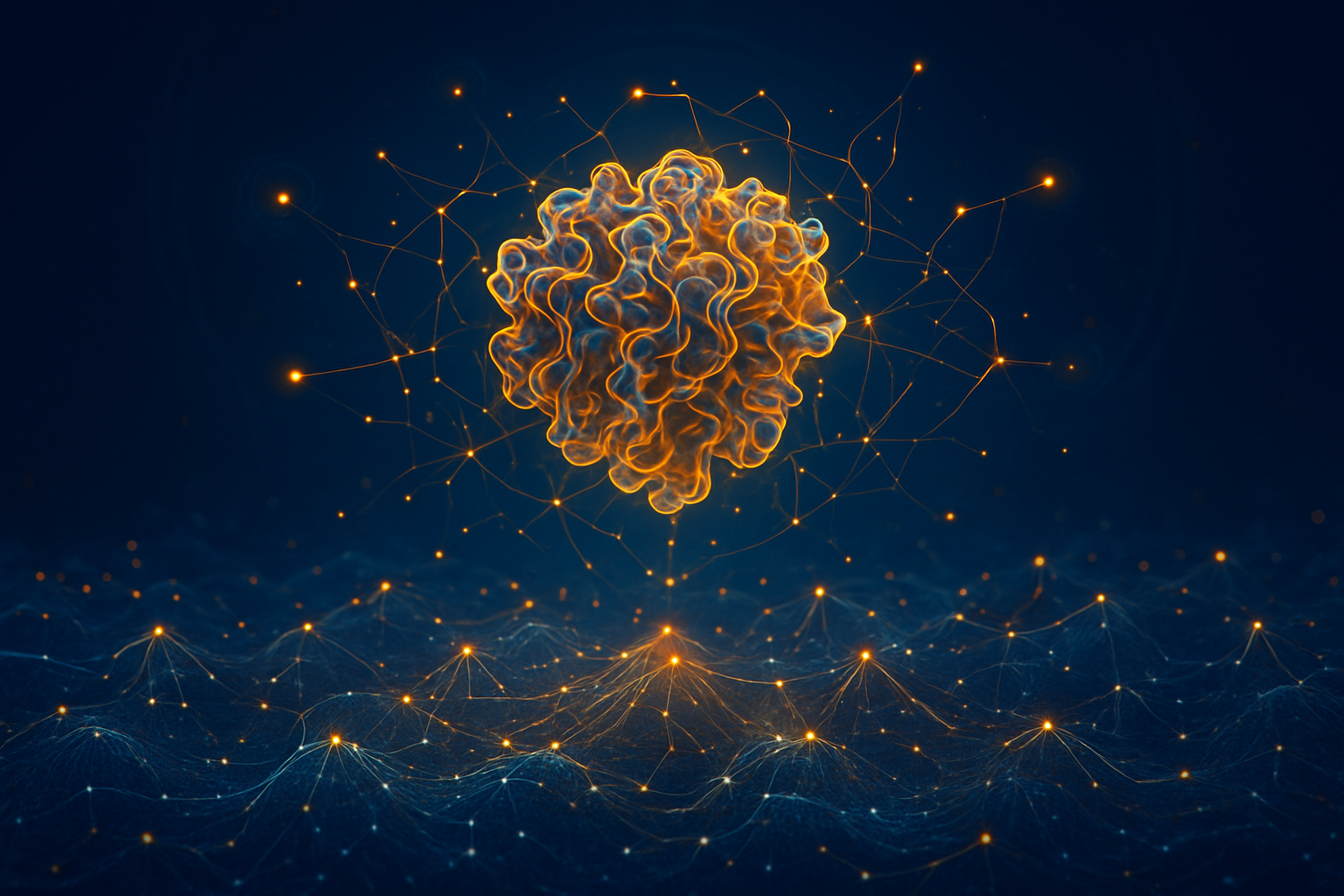
    The era of the "hard-coded" robot has officially come to an end. In a series of landmark developments culminating in early 2026, the robotics industry has undergone a fundamental shift from rigid, rule-based programming to "End-to-End" (E2E) neural networks. This transition has transformed humanoid machines from clumsy laboratory experiments into capable workers that can learn complex tasks—ranging from automotive assembly to delicate domestic chores—simply by observing human movement. By moving away from the "If-Then" logic of the past, companies like Figure AI, Tesla, and Boston Dynamics have unlocked a level of physical intelligence that was considered science fiction only three years ago.

    This breakthrough represents the "GPT moment" for physical labor. Just as Large Language Models learned to write by reading the internet, the current generation of humanoid robots is learning to move by watching the world. The immediate significance is profound: for the first time, robots can generalize their skills. A robot trained to sort laundry in a bright lab can now perform the same task in a dimly lit bedroom with different furniture, adapting in real-time to its environment without a single line of new code being written by a human engineer.

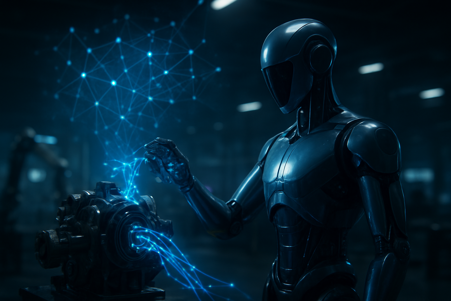
    The Architecture of Autonomy: Pixels-to-Torque

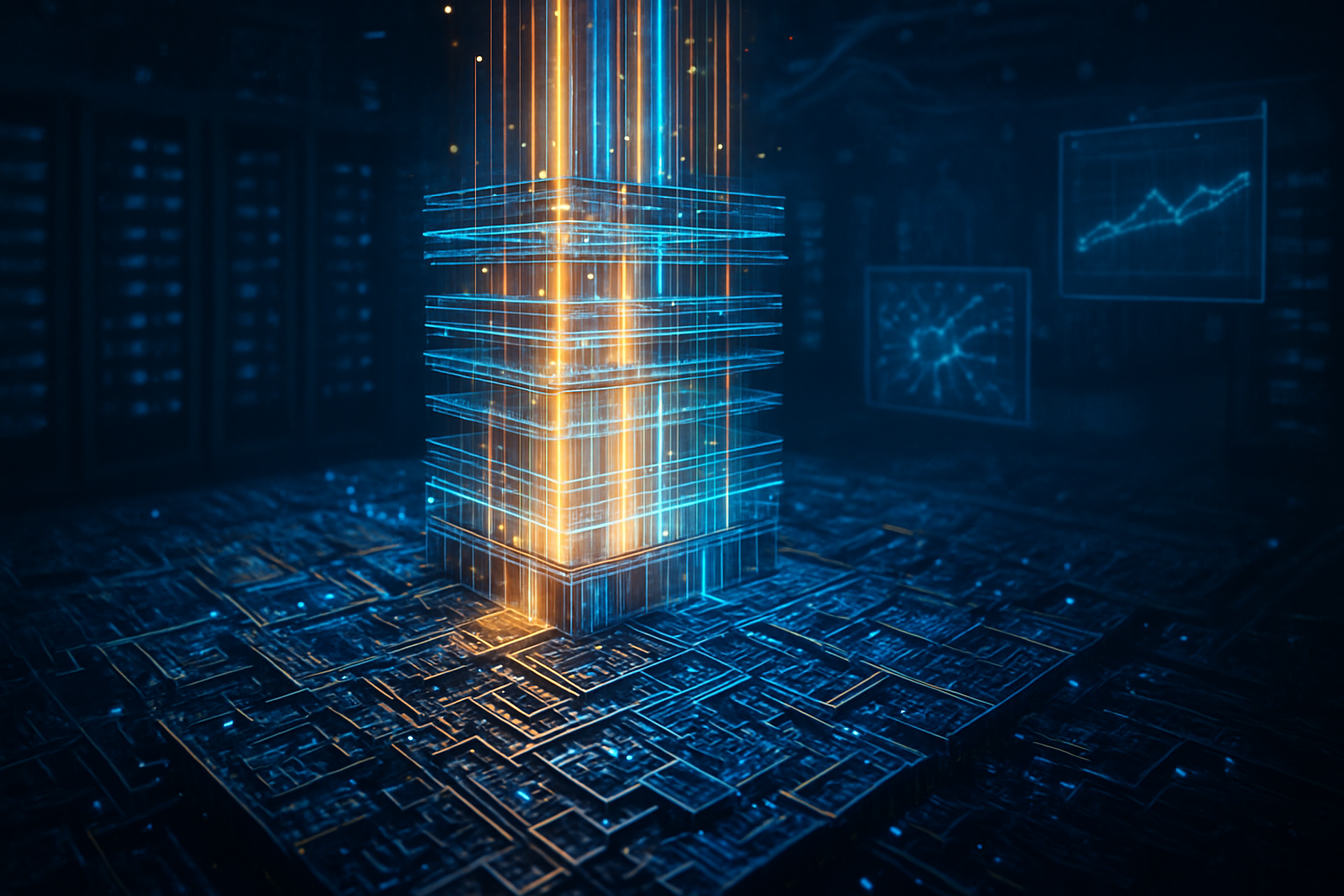
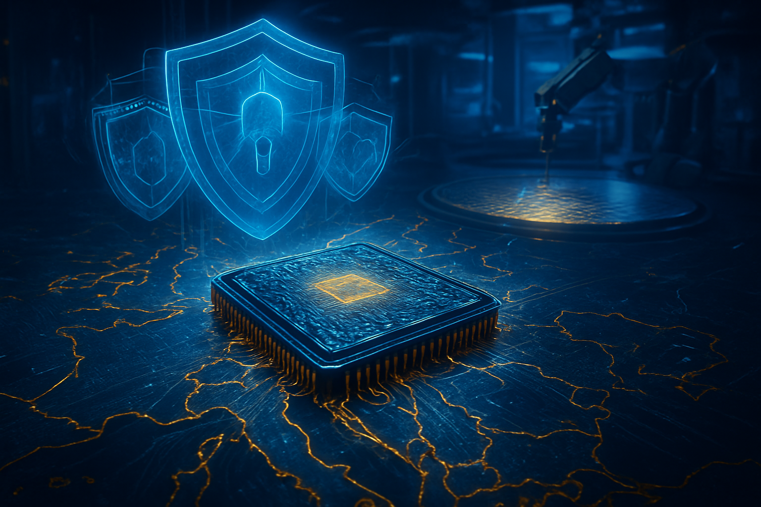
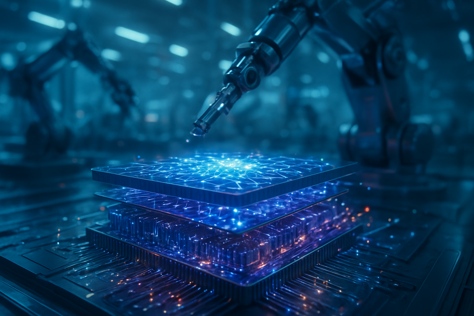
    The technical cornerstone of this revolution is the "End-to-End" neural network. Unlike the traditional "Sense-Plan-Act" paradigm—where a robot would use separate software modules for vision, path planning, and motor control—E2E systems utilize a single, massive neural network that maps visual input (pixels) directly to motor output (torque). This "Pixels-to-Torque" approach allows robots like the Figure 02 and the Tesla (NASDAQ: TSLA) Optimus Gen 2 to bypass the bottlenecks of manual coding. When Figure 02 was deployed at a BMW (ETR: BMW) manufacturing facility, it didn't require engineers to program the exact coordinates of every sheet metal part. Instead, using its "Helix" Vision-Language-Action (VLA) model, the robot observed human workers and learned the probabilistic "physics" of the task, allowing it to handle parts with 20 degrees of freedom in its hands and tactile sensors sensitive enough to detect a 3-gram weight.

    Tesla’s Optimus Gen 2, and its early 2026 successor, the Gen 3, have pushed this further by integrating the Tesla AI5 inference chip. This hardware allows the robot to run massive neural networks locally, processing 2x the frame rate with significantly lower latency than previous generations. Meanwhile, the electric Atlas from Boston Dynamics—a subsidiary of Hyundai (KRX: 005380)—has abandoned the hydraulic systems of its predecessor in favor of custom high-torque electric actuators. This hardware shift, combined with Large Behavior Models (LBMs), allows Atlas to perform 360-degree swivels and maneuvers that exceed human range of motion, all while using reinforcement learning to "self-correct" when it slips or encounters an unexpected obstacle. Industry experts note that this shift has reduced the "task acquisition time" from months of engineering to mere hours of video observation and simulation.

    The Industrial Power Play: Who Wins the Robotics Race?

    The shift to E2E neural networks has created a new competitive landscape dominated by companies with the largest datasets and the most compute power. Tesla (NASDAQ: TSLA) remains a formidable frontrunner due to its "fleet learning" advantage; the company leverages video data not just from its robots, but from millions of vehicles running Full Self-Driving (FSD) software to teach its neural networks about spatial reasoning and object permanence. This vertical integration gives Tesla a strategic advantage in scaling Optimus Gen 2 and Gen 3 across its own Gigafactories before offering them as a service to the broader manufacturing sector.

    However, the rise of Figure AI has proven that startups can compete if they have the right backers. Supported by massive investments from Microsoft (NASDAQ: MSFT) and NVIDIA (NASDAQ: NVDA), Figure has successfully moved its Figure 02 model from pilot programs into full-scale industrial deployments. By partnering with established giants like BMW, Figure is gathering high-quality "expert data" that is crucial for imitation learning. This creates a significant threat to traditional industrial robotics companies that still rely on "caged" robots and pre-defined paths. The market is now positioning itself around "Robot-as-a-Service" (RaaS) models, where the value lies not in the hardware, but in the proprietary neural weights that allow a robot to be "useful" out of the box.

    A Physical Singularity: Implications for Global Labor

    The broader significance of robots learning through observation cannot be overstated. We are witnessing the beginning of the "Physical Singularity," where the cost of manual labor begins to decouple from human demographics. As E2E neural networks allow robots to master domestic chores and factory assembly, the potential for economic disruption is vast. While this offers a solution to the chronic labor shortages in manufacturing and elder care, it also raises urgent concerns regarding job displacement for low-skill workers. Unlike previous waves of automation that targeted repetitive, high-volume tasks, E2E robotics can handle the "long tail" of irregular, complex tasks that were previously the sole domain of humans.

    Furthermore, the transition to video-based learning introduces new challenges in safety and "hallucination." Just as a chatbot might invent a fact, a robot running an E2E network might "hallucinate" a physical movement that is unsafe if it encounters a visual scenario it hasn't seen before. However, the integration of "System 2" reasoning—high-level logic layers that oversee the low-level motor networks—is becoming the industry standard to mitigate these risks. Comparisons are already being drawn to the 2012 "AlexNet" moment in computer vision; many believe 2025-2026 will be remembered as the era when AI finally gained a physical body capable of interacting with the real world as fluidly as a human.

    The Horizon: From Factories to Front Porches

    In the near term, we expect to see these humanoid robots move beyond the controlled environments of factory floors and into "semi-structured" environments like logistics hubs and retail backrooms. By late 2026, experts predict the first consumer-facing pilots for domestic "helper" robots, capable of basic tidying and grocery unloading. The primary challenge remains "Sim-to-Real" transfer—ensuring that a robot that has practiced a task a billion times in a digital twin can perform it flawlessly in a messy, unpredictable kitchen.

    Long-term, the focus will shift toward "General Purpose" embodiment. Rather than a robot that can only do "factory assembly," we are moving toward a single neural model that can be "prompted" to do anything. Imagine a robot that you can show a 30-second YouTube video of how to fix a leaky faucet, and it immediately attempts the repair. While we are not quite there yet, the trajectory of "one-shot imitation learning" suggests that the technical barriers are falling faster than even the most optimistic researchers predicted in 2024.

    A New Chapter in Human-Robot Interaction

    The breakthroughs in Figure 02, Tesla Optimus Gen 2, and the electric Atlas mark a definitive turning point in the history of technology. We have moved from a world where we had to speak the language of machines (code) to a world where machines are learning to speak the language of our movements (vision). The significance of this development lies in its scalability; once a single robot learns a task through an end-to-end network, that knowledge can be instantly uploaded to every other robot in the fleet, creating a collective intelligence that grows exponentially.

    As we look toward the coming months, the industry will be watching for the results of the first "thousand-unit" deployments in the automotive and electronics sectors. These will serve as the ultimate stress test for E2E neural networks in the real world. While the transition will not be without its growing pains—including regulatory scrutiny and safety debates—the era of the truly "smart" humanoid is no longer a future prospect; it is a present reality.


    This content is intended for informational purposes only and represents analysis of current AI developments.

    TokenRing AI delivers enterprise-grade solutions for multi-agent AI workflow orchestration, AI-powered development tools, and seamless remote collaboration platforms.
    For more information, visit https://www.tokenring.ai/.

  • The Year AI Conquered the Nobel: How 2024 Redefined the Boundaries of Science

    The Year AI Conquered the Nobel: How 2024 Redefined the Boundaries of Science

    The year 2024 will be remembered as the moment artificial intelligence transcended its reputation as a Silicon Valley novelty to become the bedrock of modern scientific discovery. In an unprecedented "double win" that sent shockwaves through the global research community, the Nobel Committees in Stockholm awarded both the Physics and Chemistry prizes to pioneers of AI. This historic recognition signaled a fundamental shift in the hierarchy of knowledge, cementing machine learning not merely as a tool for automation, but as a foundational scientific instrument capable of solving problems that had baffled humanity for generations.

    The dual awards served as a powerful validation of the "AI for Science" movement. By honoring the theoretical foundations of neural networks in Physics and the practical application of protein folding in Chemistry, the Nobel Foundation acknowledged that the digital and physical worlds are now inextricably linked. As we look back from early 2026, it is clear that these prizes were more than just accolades; they were the starting gun for a new era where the "industrialization of discovery" has become the primary driver of technological and economic value.

    The Physics of Information: From Spin Glasses to Neural Networks

    The 2024 Nobel Prize in Physics was awarded to John Hopfield and Geoffrey Hinton for foundational discoveries that enable machine learning with artificial neural networks. While the decision initially sparked debate among traditionalists, the technical justification was rooted in the deep mathematical parallels between statistical mechanics and information theory. John Hopfield’s 1982 breakthrough, the Hopfield Network, utilized the concept of "energy landscapes"—a principle borrowed from the study of magnetic spins in physics—to create a form of associative memory. By modeling neurons as "up or down" states similar to atomic spins, Hopfield demonstrated that a system could "remember" patterns by settling into a state of minimum energy.

    Geoffrey Hinton, often hailed as the "Godfather of AI," expanded this work by introducing the Boltzmann Machine. This model incorporated stochasticity (randomness) and the Boltzmann distribution—a cornerstone of thermodynamics—to allow networks to learn and generalize from data rather than just store it. Hinton’s use of "simulated annealing," where the system is "cooled" to find a global optimum, allowed these networks to escape local minima and find the most accurate representations of complex datasets. This transition from deterministic memory to probabilistic learning laid the groundwork for the deep learning revolution that powers today’s generative AI.

    The reaction from the scientific community was a mixture of awe and healthy skepticism. Figures like Max Tegmark of MIT championed the award as a recognition that AI is essentially "the physics of information." However, some purists argued that the work belonged more to computer science or mathematics. Despite the debate, the consensus by 2026 is that the award was a prescient acknowledgement of how physics-based architectures have become the "telescopes" of the 21st century, allowing scientists to see patterns in massive datasets—from CERN’s particle collisions to the discovery of exoplanets—that were previously invisible to the human eye.

    Cracking the Biological Code: AlphaFold and the Chemistry of Life

    Just days after the Physics announcement, the Nobel Prize in Chemistry was awarded to David Baker, Demis Hassabis, and John Jumper. This prize recognized a breakthrough that many consider the most significant application of AI in history: solving the "protein folding problem." For over 50 years, biologists struggled to predict how a string of amino acids would fold into a three-dimensional shape—a shape that determines a protein’s function. Hassabis and Jumper, leading the team at Google DeepMind, a subsidiary of Alphabet Inc. (NASDAQ: GOOGL), developed AlphaFold 2, an AI system that achieved near-experimental accuracy in predicting these structures.

    Technically, AlphaFold 2 represented a departure from traditional convolutional neural networks, utilizing a transformer-based architecture known as the "Evoformer." This allowed the model to process evolutionary information and spatial interactions simultaneously, iteratively refining the physical coordinates of atoms until a stable structure was reached. The impact was immediate and staggering: DeepMind released the AlphaFold Protein Structure Database, containing predictions for nearly all 200 million proteins known to science. This effectively collapsed years of expensive laboratory work into seconds of computation, democratizing structural biology for millions of researchers worldwide.

    While Hassabis and Jumper were recognized for prediction, David Baker was honored for "computational protein design." Using his Rosetta software and later AI-driven tools, Baker’s lab at the University of Washington demonstrated the ability to create entirely new proteins that do not exist in nature. This "de novo" design capability has opened the door to synthetic enzymes that can break down plastics, new classes of vaccines, and targeted drug delivery systems. Together, these laureates transformed chemistry from a descriptive science into a predictive and generative one, providing the blueprint for the "programmable biology" we are seeing flourish in 2026.

    The Industrialization of Discovery: Tech Giants and the Nobel Effect

    The 2024 Nobel wins provided a massive strategic advantage to the tech giants that funded and facilitated this research. Alphabet Inc. (NASDAQ: GOOGL) emerged as the clear winner, with the Chemistry prize serving as a definitive rebuttal to critics who claimed the company had fallen behind in the AI race. By early 2026, Google DeepMind has successfully transitioned from a research-heavy lab to a "Science-AI platform," securing multi-billion dollar partnerships with global pharmaceutical giants. The Nobel validation allowed Google to re-position its AI stack—including Gemini and its custom TPU hardware—as the premier ecosystem for high-stakes scientific R&D.

    NVIDIA (NASDAQ: NVDA) also reaped immense rewards from the "Nobel effect." Although not directly awarded, the company’s hardware was the "foundry" where these discoveries were forged. Following the 2024 awards, NVIDIA’s market capitalization surged toward the $5 trillion mark by late 2025, as the company shifted its marketing focus from "generative chatbots" to "accelerated computing for scientific discovery." Its Blackwell and subsequent Rubin architectures are now viewed as essential laboratory infrastructure, as indispensable to a modern chemist as a centrifuge or a microscope.

    Microsoft (NASDAQ: MSFT) responded by doubling down on its "agentic science" initiative. Recognizing that the next Nobel-level breakthrough would likely come from AI agents that can autonomously design and run experiments, Microsoft invested heavily in its "Stargate" supercomputing projects. By early 2026, the competitive landscape has shifted: the "AI arms race" is no longer just about who has the best chatbot, but about which company can build the most accurate "world model" capable of predicting physical reality, from material science to climate modeling.

    Beyond the Chatbot: AI as the Third Pillar of Science

    The wider significance of the 2024 Nobel Prizes lies in the elevation of AI to the "third pillar" of the scientific method, joining theory and experimentation. For centuries, science relied on human-derived hypotheses tested through physical trials. Today, AI-driven simulation and prediction have created a middle ground where "in silico" experiments can narrow down millions of possibilities to a handful of high-probability candidates. This shift has moved AI from being a "plagiarism machine" or a "homework helper" in the public consciousness to being a "truth engine" for the physical world.

    However, this transition has not been without concerns. Geoffrey Hinton used his Nobel platform to reiterate his warnings about AI safety, noting that we are moving into an era where we may "no longer understand the internal logic" of the tools we rely on for survival. There is also a growing "compute-intensity divide." As of 2026, a significant gap has emerged between "AI-rich" institutions that can afford the massive GPU clusters required for AlphaFold-scale research and "AI-poor" labs in developing nations. This has sparked a global movement toward "AI Sovereignty," with nations like the UAE and South Korea investing in national AI clouds to ensure they are not left behind in the race for scientific discovery.

    Comparisons to previous milestones, such as the discovery of the DNA double helix or the invention of the transistor, are now common. Experts argue that while the transistor gave us the ability to process information, AI gives us the ability to process complexity. The 2024 prizes recognized that human cognition has reached a limit in certain fields—like the folding of a protein or the behavior of a billion-parameter system—and that our future progress depends on a partnership with non-human intelligence.

    The 2026 Horizon: From Prediction to Synthesis

    Looking ahead through the rest of 2026, the focus is shifting from predicting what exists to synthesizing what we need. The "AlphaFold moment" in biology is being replicated in material science. We are seeing the emergence of "AlphaMat" and similar systems that can predict the properties of new crystalline structures, leading to the discovery of room-temperature superconductors and high-density batteries that were previously thought impossible. These near-term developments are expected to shave decades off the transition to green energy.

    The next major challenge being addressed is "Closed-Loop Discovery." This involves AI systems that not only predict a new molecule but also instruct robotic "cloud labs" to synthesize and test it, feeding the results back into the model without human intervention. Experts predict that by 2027, we will see the first FDA-approved drug that was entirely designed, optimized, and pre-clinically tested by an autonomous AI system. The primary hurdle remains the "veracity problem"—ensuring that AI-generated hypotheses are grounded in physical law rather than "hallucinating" scientific impossibilities.

    A Legacy Written in Silicon and Proteins

    The 2024 Nobel Prizes were a watershed moment that marked the end of AI’s "infancy" and the beginning of its "industrial era." By honoring Hinton, Hopfield, Hassabis, and Jumper, the Nobel Committee did more than just recognize individual achievement; they redefined the boundaries of what constitutes a "scientific discovery." They acknowledged that in a world of overwhelming data, the algorithm is as vital as the experiment.

    As we move further into 2026, the long-term impact of this double win is visible in every sector of the economy. AI is no longer a separate "tech" category; it is the infrastructure upon which modern biology, physics, and chemistry are built. The key takeaway for the coming months is to watch for the "Nobel Effect" to move into the regulatory and educational spheres, as universities overhaul their curricula to treat "AI Literacy" as a core requirement for every scientific discipline. The age of the "AI-Scientist" has arrived, and the world will never be the same.


    This content is intended for informational purposes only and represents analysis of current AI developments.

    TokenRing AI delivers enterprise-grade solutions for multi-agent AI workflow orchestration, AI-powered development tools, and seamless remote collaboration platforms.
    For more information, visit https://www.tokenring.ai/.

  • The Nuclear Renaissance: How Big Tech is Resurrecting Atomic Energy to Fuel the AI Boom

    The Nuclear Renaissance: How Big Tech is Resurrecting Atomic Energy to Fuel the AI Boom

    The rapid ascent of generative artificial intelligence has triggered an unprecedented surge in electricity demand, forcing the world’s largest technology companies to abandon traditional energy procurement strategies in favor of a "Nuclear Renaissance." As of early 2026, the tech industry has pivoted from being mere consumers of renewable energy to becoming the primary financiers of a new atomic age. This shift is driven by the insatiable power requirements of massive AI model training clusters, which demand gigawatt-scale, carbon-free, 24/7 "firm" power that wind and solar alone cannot reliably provide.

    This movement represents a fundamental decoupling of Big Tech from the public utility grid. Faced with aging infrastructure and five-to-seven-year wait times for new grid connections, companies like Microsoft (NASDAQ: MSFT), Amazon (NASDAQ: AMZN), and Google (NASDAQ: GOOGL) have adopted a "Bring Your Own Generation" (BYOG) strategy. By co-locating data centers directly at nuclear power sites or financing the restart of decommissioned reactors, these giants are bypassing traditional bottlenecks to ensure their AI dominance isn't throttled by a lack of electrons.

    The Resurrection of Three Mile Island and the Rise of Nuclear-Powered Data Centers

    The most symbolic milestone in this transition is the rebirth of the Crane Clean Energy Center, formerly known as Three Mile Island Unit 1. In a historic deal with Constellation Energy (NASDAQ: CEG), Microsoft has secured 100% of the plant’s 835-megawatt output for the next 20 years. As of January 2026, the facility is roughly 80% staffed, with technical refurbishments of the steam generators and turbines nearing completion. Initially slated for a 2028 restart, expedited regulatory pathways have put the plant on track to begin delivering power to Microsoft’s Mid-Atlantic data centers by early 2027. This marks the first time a retired American nuclear plant has been brought back to life specifically to serve a single corporate customer.

    While Microsoft focuses on restarts, Amazon has pursued a "behind-the-meter" strategy at the Susquehanna Steam Electric Station in Pennsylvania. Through a deal with Talen Energy (NASDAQ: TLN), Amazon acquired the Cumulus data center campus, which is physically connected to the nuclear plant. This allows Amazon to draw up to 960 megawatts of power without relying on the public transmission grid. Although the project faced significant legal challenges at the Federal Energy Regulatory Commission (FERC) throughout 2024 and 2025—with critics arguing that "co-located" data centers "free-ride" on the grid—a pivotal 5th U.S. Circuit Court ruling and new FERC rulemaking (RM26-4-000) in late 2025 have cleared a legal path for these "behind-the-fence" configurations to proceed.

    Google has taken a more diversified approach by betting on the future of Small Modular Reactors (SMRs). In a landmark partnership with Kairos Power, Google is financing the deployment of a fleet of fluoride salt-cooled high-temperature reactors totaling 500 megawatts. Unlike traditional large-scale reactors, these SMRs are designed to be factory-built and deployed closer to load centers. To bridge the gap until these reactors come online in 2030, Google also finalized a $4.75 billion acquisition of Intersect Power in late 2025. This allows Google to build "Energy Parks"—massive co-located sites featuring solar, wind, and battery storage that provide immediate, albeit variable, power while the nuclear baseload is under construction.

    Strategic Dominance and the BYOG Advantage

    The shift toward nuclear energy is not merely an environmental choice; it is a strategic necessity for market positioning. In the high-stakes arms race between OpenAI, Google, and Meta, the ability to scale compute capacity is the primary bottleneck. Companies that can secure their own dedicated power sources—the "Bring Your Own Generation" model—gain a massive competitive advantage. By bypassing the 2-terawatt backlog in the U.S. interconnection queue, these firms can bring new AI clusters online years faster than competitors who remain tethered to the public utility process.

    For energy providers like Constellation Energy and Talen Energy, the AI boom has transformed nuclear plants from aging liabilities into the most valuable assets in the energy sector. The premium prices paid by Big Tech for "firm" carbon-free energy have sent valuations for nuclear-heavy utilities to record highs. This has also triggered a consolidation wave, as tech giants seek to lock up the remaining available nuclear capacity in the United States. Analysts suggest that we are entering an era of "vertical energy integration," where the line between a technology company and a power utility becomes increasingly blurred.

    A New Paradigm for the Global Energy Landscape

    The "Nuclear Renaissance" fueled by AI has broader implications for society and the global energy landscape. The move toward "Nuclear-AI Special Economic Zones"—a concept formalized by a 2025 Executive Order—allows for the creation of high-density compute hubs on federal land, such as those near the Idaho National Lab. These zones benefit from streamlined permitting and dedicated nuclear power, creating a blueprint for how future industrial sectors might solve the energy trilemma of reliability, affordability, and sustainability.

    However, this trend has sparked concerns regarding energy equity. As Big Tech "hoards" clean energy capacity, there are growing fears that everyday ratepayers will be left with a grid that is more reliant on older, fossil-fuel-based plants, or that they will bear the costs of grid upgrades that primarily benefit data centers. The late 2025 FERC "Large Load" rulemaking was a direct response to these concerns, attempting to standardize how data centers pay for their share of the transmission system while still encouraging the "BYOG" innovation that the AI economy requires.

    The Road to 2030: SMRs and Regulatory Evolution

    Looking ahead, the next phase of the nuclear-AI alliance will be defined by the commercialization of SMRs and the implementation of the ADVANCE Act. The Nuclear Regulatory Commission (NRC) is currently under a strict 18-month mandate to review new reactor applications, a move intended to accelerate the deployment of the Kairos Power reactors and other advanced designs. Experts predict that by 2030, the first wave of SMRs will begin powering data centers in regions where the traditional grid has reached its physical limits.

    We also expect to see the "BYOG" strategy expand beyond nuclear to include advanced geothermal and fusion energy research. Microsoft and Google have already made "off-take" agreements with fusion startups, signaling that their appetite for power will only grow as AI models evolve from text-based assistants to autonomous agents capable of complex scientific reasoning. The challenge will remain the physical construction of these assets; while software scales at the speed of light, pouring concrete and forging reactor vessels still operates on the timeline of heavy industry.

    Conclusion: Atomic Intelligence

    The convergence of artificial intelligence and nuclear energy marks a definitive chapter in industrial history. We have moved past the era of "greenwashing" and into an era of "hard infrastructure" where the success of the world's most advanced software depends on the most reliable form of 20th-century hardware. The deals struck by Microsoft, Amazon, and Google in the past 18 months have effectively underwritten the future of the American nuclear industry, providing the capital and demand needed to modernize a sector that had been stagnant for decades.

    As we move through 2026, the industry will be watching the April 30th FERC deadline for final "Large Load" rules and the progress of the Crane Clean Energy Center's restart. These milestones will determine whether the "Nuclear Renaissance" can keep pace with the "AI Revolution." For now, the message from Big Tech is clear: the future of intelligence is atomic, and those who do not bring their own power may find themselves left in the dark.


    This content is intended for informational purposes only and represents analysis of current AI developments.

    TokenRing AI delivers enterprise-grade solutions for multi-agent AI workflow orchestration, AI-powered development tools, and seamless remote collaboration platforms.
    For more information, visit https://www.tokenring.ai/.

  • The $1 Trillion Horizon: Semiconductors Enter the Era of the Silicon Super-Cycle

    The $1 Trillion Horizon: Semiconductors Enter the Era of the Silicon Super-Cycle

    As of January 2, 2026, the global semiconductor industry has officially entered what analysts are calling the "Silicon Super-Cycle." Following a record-breaking 2025 that saw industry revenues soar past $800 billion, new data suggests the sector is now on an irreversible trajectory to exceed $1 trillion in annual revenue by 2030. This monumental growth is no longer speculative; it is being cemented by the relentless expansion of generative AI infrastructure, the total electrification of the automotive sector, and a new generation of "Agentic" IoT devices that require unprecedented levels of on-device intelligence.

    The significance of this milestone cannot be overstated. For decades, the semiconductor market was defined by cyclical booms and busts tied to PC and smartphone demand. However, the current era represents a structural shift where silicon has become the foundational commodity of the global economy—as essential as oil was in the 20th century. With the industry growing at a compound annual growth rate (CAGR) of over 8%, the race to $1 trillion is being led by a handful of titans who are redefining the limits of physics and manufacturing.

    The Technical Engine: 2nm, 18A, and the Rubin Revolution

    The technical landscape of 2026 is dominated by a fundamental shift in transistor architecture. For the first time in over a decade, the industry has moved away from the FinFET (Fin Field-Effect Transistor) design that powered the previous generation of electronics. Taiwan Semiconductor Manufacturing Company (NYSE: TSM), commonly known as TSMC, has successfully ramped up its 2nm (N2) process, utilizing Nanosheet Gate-All-Around (GAA) transistors. This transition allows for a 15% performance boost or a 30% reduction in power consumption compared to the 3nm nodes of 2024.

    Simultaneously, Intel (NASDAQ: INTC) has achieved a major milestone with its 18A (1.8nm) process, which entered high-volume production at its Arizona facilities this month. The 18A node introduces "PowerVia," the industry’s first implementation of backside power delivery, which separates the power lines from the data lines on a chip to reduce interference and improve efficiency. This technical leap has allowed Intel to secure major foundry customers, including a landmark partnership with NVIDIA (NASDAQ: NVDA) for specialized AI components.

    On the architectural front, NVIDIA has just begun shipping its "Rubin" R100 GPUs, the successor to the Blackwell line. The Rubin architecture is the first to fully integrate the HBM4 (High Bandwidth Memory 4) standard, which doubles the memory bus width to 2048-bit and provides a staggering 2.0 TB/s of peak throughput per stack. This leap in memory performance is critical for "Agentic AI"—autonomous AI systems that require massive local memory to process complex reasoning tasks in real-time without constant cloud polling.

    The Beneficiaries: NVIDIA’s Dominance and the Foundry Wars

    The primary beneficiary of this $1 trillion march remains NVIDIA, which briefly touched a $5 trillion market capitalization in late 2025. By controlling over 90% of the AI accelerator market, NVIDIA has effectively become the gatekeeper of the AI era. However, the competitive landscape is shifting. Advanced Micro Devices (NASDAQ: AMD) has gained significant ground with its MI400 series, capturing nearly 15% of the data center market by offering a more open software ecosystem compared to NVIDIA’s proprietary CUDA platform.

    The "Foundry Wars" have also intensified. While TSMC still holds a dominant 70% market share, the resurgence of Intel Foundry and the steady progress of Samsung (KRX: 005930) have created a more fragmented market. Samsung recently secured a $16.5 billion deal with Tesla (NASDAQ: TSLA) to produce next-generation Full Self-Driving (FSD) chips using its 3nm GAA process. Meanwhile, Broadcom (NASDAQ: AVGO) and Marvell (NASDAQ: MRVL) are seeing record revenues as "hyperscalers" like Google and Amazon shift toward custom-designed AI ASICs (Application-Specific Integrated Circuits) to reduce their reliance on off-the-shelf GPUs.

    This shift toward customization is disrupting the traditional "one-size-fits-all" chip model. Startups specializing in "Edge AI" are finding fertile ground as the market moves from training large models in the cloud to running them on local devices. Companies that can provide high-performance, low-power silicon for the "Intelligence of Things" are increasingly becoming acquisition targets for tech giants looking to vertically integrate their hardware stacks.

    The Global Stakes: Geopolitics and the Environmental Toll

    As the semiconductor industry scales toward $1 trillion, it has become the primary theater of global geopolitical competition. The U.S. CHIPS Act has transitioned from a funding phase to an operational one, with several leading-edge "mega-fabs" now online in the United States. This has created a strategic buffer, yet the world remains heavily dependent on the "Silicon Shield" of Taiwan. In late 2025, simulated blockades in the Taiwan Strait sent shockwaves through the market, highlighting that even a minor disruption in the region could risk a $500 billion hit to the global economy.

    Beyond geopolitics, the environmental impact of a $1 trillion industry is coming under intense scrutiny. A single modern mega-fab in 2026 consumes as much as 10 million gallons of ultrapure water per day and requires energy levels equivalent to a small city. The transition to 2nm and 1.8nm nodes has increased energy intensity by nearly 3.5x compared to legacy nodes. In response, the industry is pivoting toward "Circular Silicon" initiatives, with TSMC and Intel pledging to recycle 85% of their water and transition to 100% renewable energy by 2030 to mitigate regulatory pressure and resource scarcity.

    This environmental friction is a new phenomenon for the industry. Unlike the software booms of the past, the semiconductor super-cycle is tied to physical constraints—land, water, power, and rare earth minerals. The ability of a company to secure "green" manufacturing capacity is becoming as much of a competitive advantage as the transistor density of its chips.

    The Road to 2030: Edge AI and the Intelligence of Things

    Looking ahead, the next four years will be defined by the migration of AI from the data center to the "Edge." While the current revenue surge is driven by massive server farms, the path to $1 trillion will be paved by the billions of devices in our pockets, homes, and cars. We are entering the era of the "Intelligence of Things" (IoT 2.0), where every sensor and appliance will possess enough local compute power to run sophisticated AI agents.

    In the automotive sector, the semiconductor content per vehicle is expected to double by 2030. Modern Electric Vehicles (EVs) are essentially data centers on wheels, requiring high-power silicon carbide (SiC) semiconductors for power management and high-end SoCs (System on a Chip) for autonomous navigation. Qualcomm (NASDAQ: QCOM) is positioning itself as a leader in this space, leveraging its mobile expertise to dominate the "Digital Cockpit" market.

    Experts predict that the next major breakthrough will involve Silicon Photonics—using light instead of electricity to move data between chips. This technology, expected to hit the mainstream by 2028, could solve the "interconnect bottleneck" that currently limits the scale of AI clusters. As we approach the end of the decade, the integration of quantum-classical hybrid chips is also expected to emerge, providing a new frontier for specialized scientific computing.

    A New Industrial Bedrock

    The semiconductor industry's journey to $1 trillion is a testament to the central role of hardware in the AI revolution. The key takeaway from early 2026 is that the industry has successfully navigated the transition to GAA transistors and localized manufacturing, creating a more resilient, albeit more expensive, global supply chain. The "Silicon Super-Cycle" is no longer just about faster computers; it is about the infrastructure of modern life.

    In the history of technology, this period will likely be remembered as the moment semiconductors surpassed the automotive and energy industries in strategic importance. The long-term impact will be a world where intelligence is "baked in" to every physical object, driven by the chips currently rolling off the assembly lines in Hsinchu, Phoenix, and Magdeburg.

    In the coming weeks and months, investors and industry watchers should keep a eye on the yield rates of 2nm production and the first real-world benchmarks of NVIDIA’s Rubin GPUs. These metrics will determine which companies will capture the lion's share of the final $200 billion climb to the trillion-dollar mark.


    This content is intended for informational purposes only and represents analysis of current AI developments.

    TokenRing AI delivers enterprise-grade solutions for multi-agent AI workflow orchestration, AI-powered development tools, and seamless remote collaboration platforms.
    For more information, visit https://www.tokenring.ai/.

  • Breaking the Memory Wall: 3D DRAM Breakthroughs Signal a New Era for AI Supercomputing

    Breaking the Memory Wall: 3D DRAM Breakthroughs Signal a New Era for AI Supercomputing

    As of January 2, 2026, the artificial intelligence industry has reached a critical hardware inflection point. For years, the rapid advancement of Large Language Models (LLMs) and generative AI has been throttled by the "Memory Wall"—a performance bottleneck where processor speeds far outpace the ability of memory to deliver data. This week, a series of breakthroughs in high-density 3D DRAM architecture from the world’s leading semiconductor firms has signaled that this wall is finally coming down, paving the way for the next generation of trillion-parameter AI models.

    The transition from traditional planar (2D) DRAM to vertical 3D architectures is no longer a laboratory experiment; it has entered the early stages of mass production and validation. Industry leaders Samsung Electronics (KRX: 005930), SK Hynix (KRX: 000660), and Micron Technology (NASDAQ: MU) have all unveiled refined 3D roadmaps that promise to triple memory density while drastically reducing the energy footprint of AI data centers. This development is widely considered the most significant shift in memory technology since the industry-wide transition to 3D NAND a decade ago.

    The Architecture of the "Nanoscale Skyscraper"

    The technical core of this breakthrough lies in the move from the traditional 6F² cell structure to a more compact 4F² configuration. In 2D DRAM, memory cells are laid out horizontally, but as manufacturers pushed toward sub-10nm nodes, physical limits made further shrinking impossible. The 4F² structure, enabled by Vertical Channel Transistors (VCT), allows engineers to stack the capacitor directly on top of the source, gate, and drain. By standing the transistors upright like "nanoscale skyscrapers," manufacturers can reduce the cell area by roughly 30%, allowing for significantly more capacity in the same physical footprint.

    A major technical hurdle addressed in early 2026 is the management of leakage and heat. Samsung and SK Hynix have both demonstrated the use of Indium Gallium Zinc Oxide (IGZO) as a channel material. Unlike traditional silicon, IGZO has an extremely low leakage current, which allows for data retention times of over 450 seconds—a massive improvement over the milliseconds seen in standard DRAM. Furthermore, the debut of HBM4 (High Bandwidth Memory 4) has introduced a 2048-bit interface, doubling the bandwidth of the previous generation. This is achieved through "hybrid bonding," a process that eliminates traditional micro-bumps and bonds memory directly to logic chips using copper-to-copper connections, reducing the distance data travels from millimeters to microns.

    A High-Stakes Arms Race for AI Dominance

    The shift to 3D DRAM has ignited a fierce competitive struggle among the "Big Three" memory makers and their primary customers. SK Hynix, which currently holds a dominant market share in the HBM sector, has solidified its lead through a strategic alliance with Taiwan Semiconductor Manufacturing Company (NYSE: TSM) to refine the hybrid bonding process. Meanwhile, Samsung is leveraging its unique position as a vertically integrated giant—spanning memory, foundry, and logic—to offer "turnkey" AI solutions that integrate 3D DRAM directly with their own AI accelerators, aiming to bypass the packaging leads held by its rivals.

    For chip giants like NVIDIA (NASDAQ: NVDA) and Advanced Micro Devices (NASDAQ: AMD), these breakthroughs are the lifeblood of their 2026 product cycles. NVIDIA’s newly announced "Rubin" architecture is designed specifically to utilize HBM4, targeting bandwidths exceeding 2.8 TB/s. AMD is positioning its Instinct MI400 series as a "bandwidth king," utilizing 3D-stacked DRAM to offer a projected 30% improvement in total cost of ownership (TCO) for hyperscalers. Cloud providers like Amazon (NASDAQ: AMZN), Microsoft (NASDAQ: MSFT), and Alphabet (NASDAQ: GOOGL) are the ultimate beneficiaries, as 3D DRAM allows them to cram more intelligence into each rack of their "AI Superfactories" while staying within the rigid power constraints of modern electrical grids.

    Shattering the Memory Wall and the Sustainability Gap

    Beyond the technical specifications, the broader significance of 3D DRAM lies in its potential to solve the AI industry's looming energy crisis. Moving data between memory and processors is one of the most energy-intensive tasks in a data center. By stacking memory vertically and placing it closer to the compute engine, 3D DRAM is projected to reduce the energy required per bit of data moved by 40% to 70%. In an era where a single AI training cluster can consume as much power as a small city, these efficiency gains are not just a luxury—they are a requirement for the continued growth of the sector.

    However, the transition is not without its concerns. The move to 3D DRAM mirrors the complexity of the 3D NAND transition but with much higher stakes. Unlike NAND, DRAM requires a capacitor to store charge, which is notoriously difficult to stack vertically without sacrificing stability. This has led to a "capacitor hurdle" that some experts fear could lead to lower manufacturing yields and higher initial prices. Furthermore, the extreme thermal density of stacking 16 or more layers of active silicon creates "thermal crosstalk," where heat from the bottom logic die can degrade the data stored in the memory layers above. This is forcing a mandatory shift toward liquid cooling solutions in nearly all high-end AI installations.

    The Road to Monolithic 3D and 2030

    Looking ahead, the next two to three years will see the refinement of "Custom HBM," where memory is no longer a commodity but is co-designed with specific AI architectures like Google’s TPUs or AWS’s Trainium chips. By 2028, experts predict the arrival of HBM4E, which will push stacking to 20 layers and incorporate "Processing-in-Memory" (PiM) capabilities, allowing the memory itself to perform basic AI inference tasks. This would further reduce the need to move data, effectively turning the memory stack into a distributed computer.

    The ultimate goal, expected around 2030, is Monolithic 3D DRAM. This would move away from stacking separate finished dies and instead build dozens of memory layers on a single wafer from the ground up. Such an advancement would allow for densities of 512GB to 1TB per chip, potentially bringing the power of today's supercomputers to consumer-grade devices. The primary challenge remains the development of "aspect ratio etching"—the ability to drill perfectly vertical holes through hundreds of layers of silicon without a single micrometer of deviation.

    A Tipping Point in Semiconductor History

    The breakthroughs in 3D DRAM architecture represent a fundamental shift in how humanity builds the machines that think. By moving into the third dimension, the semiconductor industry has found a way to extend the life of Moore's Law and provide the raw data throughput necessary for the next leap in artificial intelligence. This is not merely an incremental update; it is a re-engineering of the very foundation of computing.

    In the coming weeks and months, the industry will be watching for the first "qualification" reports of 16-layer HBM4 stacks from NVIDIA and the results of Samsung’s VCT verification phase. As these technologies move from the lab to the fab, the gap between those who can master 3D packaging and those who cannot will likely define the winners and losers of the AI era for the next decade. The "Memory Wall" is falling, and what lies on the other side is a world of unprecedented computational scale.


    This content is intended for informational purposes only and represents analysis of current AI developments.

    TokenRing AI delivers enterprise-grade solutions for multi-agent AI workflow orchestration, AI-powered development tools, and seamless remote collaboration platforms.
    For more information, visit https://www.tokenring.ai/.

  • The Fortress of Silicon: Europe’s Bold Pivot to Sovereign Chip Security Reshapes Global AI Trade

    The Fortress of Silicon: Europe’s Bold Pivot to Sovereign Chip Security Reshapes Global AI Trade

    As of January 2, 2026, the global semiconductor landscape has undergone a tectonic shift, driven by the European Union’s aggressive "Silicon Sovereignty" initiative. What began as a response to pandemic-era supply chain vulnerabilities has evolved into a comprehensive security-first doctrine. By implementing the first enforcement phase of the Cyber Resilience Act (CRA) and the revamped EU Chips Act 2.0, Brussels has effectively erected a "Silicon Shield," prioritizing the security and traceability of high-tech components over the raw volume of production. This movement is not merely about manufacturing; it is a fundamental reconfiguration of the global trade landscape, mandating that any silicon entering the European market meets stringent "Security-by-Design" standards that are now setting a new global benchmark.

    The immediate significance of this crackdown lies in its focus on the "hardware root of trust." Unlike previous decades where security was largely a software-level concern, the EU now legally mandates that microprocessors and sensors contain immutable security features at the silicon level. This has created a bifurcated global market: chips destined for Europe must undergo rigorous third-party assessments to earn a "CE" security mark, while less secure components are increasingly relegated to secondary markets. For the artificial intelligence industry, this means that the hardware running the next generation of LLMs and edge devices is becoming more transparent, more secure, and significantly more integrated into the European geopolitical sphere.

    Technically, the push for Silicon Sovereignty is anchored by the full operational status of five major "Pilot Lines" across the continent, coordinated by the Chips for Europe initiative. The NanoIC line at imec in Belgium is now testing sub-2nm architectures, while the FAMES line at CEA-Leti in France is pioneering Fully Depleted Silicon-on-Insulator (FD-SOI) technology. These advancements differ from previous approaches by moving away from general-purpose logic and toward specialized, energy-efficient "Green AI" hardware. The focus is on low-power inference at the edge, where security is baked into the physical gate architecture to prevent side-channel attacks and unauthorized data exfiltration—a critical requirement for the EU’s strict data privacy laws.

    The Cyber Resilience Act has introduced a technical mandate for "Active Vulnerability Reporting," requiring chipmakers to report exploited hardware flaws to the European Union Agency for Cybersecurity (ENISA) within 24 hours. This level of transparency is unprecedented in the semiconductor industry, which has traditionally guarded hardware errata as trade secrets. Industry experts from the AI research community have noted that these standards are forcing a shift from "black box" hardware to "verifiable silicon." By utilizing RISC-V open-source architectures for sovereign AI accelerators, European researchers are attempting to eliminate the "backdoor" risks often associated with proprietary instruction set architectures.

    Initial reactions from the industry have been a mix of praise for the enhanced security and concern over the cost of compliance. While the European Design Platform has successfully onboarded over 100 startups by providing low-barrier access to Electronic Design Automation (EDA) tools, the cost of third-party security audits for "Critical Class II" products—which include most AI-capable microprocessors—has added a significant layer of overhead. Nevertheless, the consensus among security experts is that this "Iron Curtain of Silicon" is a necessary evolution in an era where hardware-level vulnerabilities can compromise entire national infrastructures.

    This shift has created a new hierarchy among tech giants and specialized semiconductor firms. ASML Holding N.V. (NASDAQ: ASML) has emerged as the linchpin of this strategy, with the Dutch government fully aligning its export licenses for High-NA EUV lithography systems with the EU’s broader economic security goals. This alignment has effectively restricted the most advanced manufacturing capabilities to a "G7+ Chip Coalition," leaving competitors in non-aligned regions struggling to keep pace with the sub-2nm transition. Meanwhile, STMicroelectronics N.V. (NYSE: STM) and NXP Semiconductors N.V. (NASDAQ: NXPI) have seen their market positions bolstered as the primary providers of secure, automotive-grade AI chips that meet the new EU mandates.

    Intel Corporation (NASDAQ: INTC) has faced a more complex path; while its massive "Magdeburg" project in Germany saw delays throughout 2025, its Fab 34 in Leixlip, Ireland, has become the lead European hub for high-volume 3nm production. This has allowed Intel to position itself as a "sovereign-friendly" foundry for European AI startups like Mistral AI and Aleph Alpha. Conversely, Taiwan Semiconductor Manufacturing Company (NYSE: TSM) has had to adapt its European strategy, focusing heavily on specialized 12nm and 16nm nodes for the industrial and automotive sectors in its Dresden facility to satisfy the EU’s demand for local, secure supply chains for "Smart Power" applications.

    The competitive implications are profound for major AI labs. Companies that rely on highly centralized, non-transparent hardware may find themselves locked out of European government and critical infrastructure contracts. This has spurred a wave of strategic partnerships where software giants are co-designing hardware with European firms to ensure compliance. For instance, the integration of "Sovereign LLMs" directly onto NXP’s secure automotive platforms has become a blueprint for how AI companies can maintain a foothold in the European market by prioritizing local security standards over raw processing speed.

    Beyond the technical and corporate spheres, the "Silicon Sovereignty" movement represents a major milestone in the history of AI and global trade. It marks the end of the "borderless silicon" era, where components were designed in one country, manufactured in another, and packaged in a third with little regard for the geopolitical implications of the underlying hardware. This new era of "Technological Statecraft" mirrors the Cold War-era export controls but with a modern focus on AI safety and cybersecurity. The EU's move is a direct challenge to the dominance of both US-centric and China-centric supply chains, attempting to carve out a third way that prioritizes democratic values and data sovereignty.

    However, this fragmentation raises concerns about the "Balkanization" of the AI industry. If different regions mandate vastly different hardware security standards, the cost of developing global AI products could skyrocket. There is also the risk of a "security-performance trade-off," where the overhead required for real-time hardware monitoring and encrypted memory paths could make European-compliant chips slower or more expensive than their less-regulated counterparts. Comparisons are being made to the GDPR’s impact on the software industry; while initially seen as a burden, it eventually became a global gold standard that other regions felt compelled to emulate.

    The wider significance also touches on the environmental impact of AI. By focusing on "Green AI" and energy-efficient edge computing, Europe is attempting to lead the transition to a more sustainable AI infrastructure. The EU Chips Act’s support for Wide-Bandgap semiconductors, such as Silicon Carbide and Gallium Nitride, is a crucial part of this, enabling more efficient power conversion for the massive data centers required to train and run large-scale AI models. This "Green Sovereignty" adds a moral and environmental dimension to the geopolitical struggle for chip dominance.

    Looking ahead to the rest of 2026 and beyond, the next major milestone will be the full implementation of the Silicon Box (a €3.2B chiplet fab in Italy), which aims to bring advanced packaging capabilities back to European soil. This is critical because, until now, even chips designed and etched in Europe often had to be sent to Asia for the final "back-end" processing, creating a significant security gap. Once this facility is operational, the EU will possess a truly end-to-end sovereign supply chain for advanced AI chiplets.

    Experts predict that the focus will soon shift from logic chips to "Photonic Integrated Circuits" (PICs). The PIXEurope pilot line is expected to yield the first commercially viable light-based AI accelerators by 2027, which could offer a 10x improvement in energy efficiency for neural network processing. The challenge will be scaling these technologies and ensuring that the European ecosystem can attract enough high-tier talent to compete with the massive R&D budgets of Silicon Valley. Furthermore, the ongoing "Lithography War" will remain a flashpoint, as China continues to invest heavily in domestic alternatives to ASML’s technology, potentially leading to a complete decoupling of the global semiconductor market.

    In summary, Europe's crackdown on semiconductor security and its push for Silicon Sovereignty have fundamentally altered the trajectory of the AI industry. By mandating "Security-by-Design" and investing in a localized, secure supply chain, the EU has moved from a position of dependency to one of strategic influence. The key takeaways from this transition are the elevation of hardware security to a legal requirement, the rise of specialized "Green AI" architectures, and the emergence of a "G7+ Chip Coalition" that uses high-tech monopolies like High-NA EUV as diplomatic leverage.

    This development will likely be remembered as the moment when the geopolitical reality of AI hardware finally caught up with the borderless ambitions of AI software. As we move further into 2026, the industry must watch for the first wave of CRA-related enforcement actions and the progress of the "AI Factories" being built under the EuroHPC initiative. The "Fortress of Silicon" is now under construction, and its walls are being built with the dual bricks of security and sovereignty, forever changing how the world trades in the intelligence of the future.


    This content is intended for informational purposes only and represents analysis of current AI developments.

    TokenRing AI delivers enterprise-grade solutions for multi-agent AI workflow orchestration, AI-powered development tools, and seamless remote collaboration platforms.
    For more information, visit https://www.tokenring.ai/.

  • The CoWoS Crunch Ends: TSMC Unleashes Massive Packaging Expansion to Power the 2026 AI Supercycle

    The CoWoS Crunch Ends: TSMC Unleashes Massive Packaging Expansion to Power the 2026 AI Supercycle

    As of January 2, 2026, the global semiconductor landscape has reached a definitive turning point. After two years of "packaging-bound" constraints that throttled the supply of high-end artificial intelligence processors, Taiwan Semiconductor Manufacturing Company (NYSE:TSM) has officially entered a new era of hyper-scale production. By aggressively expanding its Chip on Wafer on Substrate (CoWoS) capacity, TSMC is finally clearing the bottlenecks that once forced lead times for AI servers to stretch beyond 50 weeks, signaling a massive shift in how the industry builds the engines of the generative AI revolution.

    This expansion is not merely an incremental upgrade; it is a structural transformation of the silicon supply chain. By the end of 2025, TSMC successfully nearly doubled its CoWoS output to 75,000 wafers per month, and current projections for 2026 suggest the company will hit a staggering 130,000 wafers per month by year-end. This surge in capacity is specifically designed to meet the insatiable appetite for NVIDIA’s Blackwell and upcoming Rubin architectures, as well as AMD’s MI350 series, ensuring that the next generation of Large Language Models (LLMs) and autonomous systems are no longer held back by the physical limits of chip assembly.

    The Technical Evolution of Advanced Packaging

    The technical evolution of advanced packaging has become the new frontline of Moore’s Law. While traditional chip scaling—making transistors smaller—has slowed, TSMC’s CoWoS technology allows multiple "chiplets" to be interconnected on a single interposer, effectively creating a "superchip" that behaves like a single, massive processor. The current industry standard has shifted from the mature CoWoS-S (Standard) to the more complex CoWoS-L (Local Silicon Interconnect). CoWoS-L utilizes an RDL interposer with embedded silicon bridges, allowing for modular designs that can exceed the traditional "reticle limit" of a single silicon wafer.

    This shift is critical for the latest hardware. NVIDIA (NASDAQ:NVDA) is utilizing CoWoS-L for its Blackwell (B200) GPUs to connect two high-performance logic dies with eight stacks of High Bandwidth Memory (HBM3e). Looking ahead to the Rubin (R100) architecture, which is entering trial production in early 2026, the requirements become even more extreme. Rubin will adopt a 3nm process and a massive 4x reticle size interposer, integrating up to 12 stacks of next-generation HBM4. Without the capacity expansion at TSMC’s new facilities, such as the massive AP8 plant in Tainan, these chips would be nearly impossible to manufacture at scale.

    Industry experts note that this transition represents a departure from the "monolithic" chip era. By using CoWoS, manufacturers can mix and match different components—such as specialized AI accelerators, I/O dies, and memory—onto a single package. This approach significantly improves yield rates, as it is easier to manufacture several small, perfect dies than one giant, flawless one. The AI research community has lauded this development, as it directly enables the multi-terabyte-per-second memory bandwidth required for the trillion-parameter models currently under development.

    Competitive Implications for the AI Giants

    The primary beneficiary of this capacity surge remains NVIDIA, which has reportedly secured over 60% of TSMC’s total 2026 CoWoS output. This strategic "lock-in" gives NVIDIA a formidable moat, allowing it to maintain its dominant market share by ensuring its customers—ranging from hyperscalers like Microsoft and Google to sovereign AI initiatives—can actually receive the hardware they order. However, the expansion also opens the door for Advanced Micro Devices (NASDAQ:AMD), which is using TSMC’s SoIC (System-on-Integrated-Chip) and CoWoS-S technologies for its MI325 and MI350X accelerators to challenge NVIDIA’s performance lead.

    The competitive landscape is further complicated by the entry of Broadcom (NASDAQ:AVGO) and Marvell Technology (NASDAQ:MRVL), both of which are leveraging TSMC’s advanced packaging to build custom AI ASICs (Application-Specific Integrated Circuits) for major cloud providers. As packaging capacity becomes more available, the "premium" price of AI compute may begin to stabilize, potentially disrupting the high-margin environment that has fueled record profits for chipmakers over the last 24 months.

    Meanwhile, Intel (NASDAQ:INTC) is attempting to position its Foundry Services as a viable alternative, promoting its EMIB (Embedded Multi-die Interconnect Bridge) and Foveros technologies. While Intel has made strides in securing smaller contracts, the high cost of porting designs away from TSMC’s ecosystem has kept the largest AI players loyal to the Taiwanese giant. Samsung (KRX:005930) has also struggled to gain ground; despite offering "turnkey" solutions that combine HBM production with packaging, yield issues on its advanced nodes have allowed TSMC to maintain its lead.

    Broader Significance for the AI Landscape

    The broader significance of this development lies in the realization that the "compute" bottleneck has been replaced by a "connectivity" bottleneck. In the early 2020s, the industry focused on how many transistors could fit on a chip. In 2026, the focus has shifted to how fast those chips can talk to each other and their memory. TSMC’s expansion of CoWoS is the physical manifestation of this shift, marking a transition into the "3D Silicon" era where the vertical and horizontal integration of chips is as important as the lithography used to print them.

    This trend has profound geopolitical implications. The concentration of advanced packaging capacity in Taiwan remains a point of concern for global supply chain resilience. While TSMC is expanding its footprint in Arizona and Japan, the most cutting-edge "CoW" (Chip-on-Wafer) processes remain centered in facilities like the new Chiayi AP7 plant. This ensures that Taiwan remains the indispensable "silicon shield" of the global economy, even as Western nations push for more localized semiconductor manufacturing.

    Furthermore, the environmental impact of these massive packaging facilities is coming under scrutiny. Advanced packaging requires significant amounts of ultrapure water and electricity, leading to localized tensions in regions like Chiayi. As the AI industry continues to scale, the sustainability of these manufacturing hubs will become a central theme in corporate social responsibility reports and government regulations, mirroring the debates currently surrounding the energy consumption of AI data centers.

    Future Developments in Silicon Integration

    Looking toward the near-term future, the next major milestone will be the widespread adoption of glass substrates. While current CoWoS technology relies on silicon or organic interposers, glass offers superior thermal stability and flatter surfaces, which are essential for the ultra-fine interconnects required for HBM4 and beyond. TSMC and its partners are already conducting pilot runs with glass substrates, with full-scale integration expected by late 2027 or 2028.

    Another area of rapid development is the integration of optical interconnects directly into the package. As electrical signals struggle to travel across large substrates without significant power loss, "Silicon Photonics" will allow chips to communicate using light. This will enable the creation of "warehouse-scale" computers where thousands of GPUs function as a single, unified processor. Experts predict that the first commercial AI chips featuring integrated co-packaged optics (CPO) will begin appearing in high-end data centers within the next 18 to 24 months.

    A Comprehensive Wrap-Up

    In summary, TSMC’s aggressive expansion of its CoWoS capacity is the final piece of the puzzle for the current AI boom. By resolving the packaging bottlenecks that defined 2024 and 2025, the company has cleared the way for a massive influx of high-performance hardware. The move cements TSMC’s role as the foundation of the AI era and underscores the reality that advanced packaging is no longer a "back-end" process, but the primary driver of semiconductor innovation.

    As we move through 2026, the industry will be watching closely to see if this surge in supply leads to a cooling of the AI market or if the demand for even larger models will continue to outpace production. For now, the "CoWoS Crunch" is effectively over, and the race to build the next generation of artificial intelligence has entered a high-octane new phase.


    This content is intended for informational purposes only and represents analysis of current AI developments.

    TokenRing AI delivers enterprise-grade solutions for multi-agent AI workflow orchestration, AI-powered development tools, and seamless remote collaboration platforms.
    For more information, visit https://www.tokenring.ai/.

  • Samsung Cements AI Dominance: Finalizes Land Deal for Massive $250 Billion Yongin Mega-Fab

    Samsung Cements AI Dominance: Finalizes Land Deal for Massive $250 Billion Yongin Mega-Fab

    In a move that signals a seismic shift in the global semiconductor landscape, Samsung Electronics (KRX: 005930) has officially finalized a landmark land deal for its massive "Mega-Fab" semiconductor cluster in Yongin, South Korea. The agreement, signed on December 19, 2025, and formally announced to the global market on January 2, 2026, marks the transition from speculative planning to concrete execution for what is slated to be the world’s largest high-tech manufacturing facility. By securing the 7.77 million square meter site, Samsung has effectively anchored its long-term strategy to reclaim the lead in the "AI Supercycle," positioning itself as the primary alternative to the current dominance of Taiwanese manufacturing.

    The finalization of this deal is more than a real estate transaction; it is a strategic maneuver designed to insulate Samsung’s future production from the geographic and geopolitical constraints facing its rivals. As the demand for generative AI and high-performance computing (HPC) continues to outpace global supply, the Yongin cluster represents South Korea’s "all-in" bet on maintaining its status as a semiconductor superpower. For Samsung, the project is the physical manifestation of its "One-Stop Solution" strategy, aiming to integrate logic chip foundry services, advanced HBM4 memory production, and next-generation packaging under a single, massive roof.

    A Technical Titan: 2nm GAA and the HBM4 Integration

    The technical specifications of the Yongin Mega-Fab are staggering in their scale and ambition. Spanning 7.77 million square meters in the Idong-eup and Namsa-eup regions, the site will eventually house six world-class semiconductor fabrication plants (fabs). Samsung has committed an initial 360 trillion won (approximately $251.2 billion) to the project, a figure that industry experts expect to climb as the facility integrates the latest High-NA Extreme Ultraviolet (EUV) lithography machines required for sub-2nm manufacturing. This investment is specifically targeted at the mass production of 2nm Gate-All-Around (GAA) transistors and future 1.4nm nodes, which offer significant improvements in power efficiency and performance over the FinFET architectures used by many competitors.

    What sets the Yongin cluster apart from existing facilities, such as Samsung’s Pyeongtaek site or TSMC’s (NYSE: TSM) Hsinchu Science Park, is its focus on "vertical AI integration." Unlike previous generations of fabs that specialized in either memory or logic, the Yongin Mega-Fab is designed to facilitate the "turnkey" production of AI accelerators. This involves the simultaneous manufacturing of the logic die and the 6th-generation High Bandwidth Memory (HBM4) on the same campus. By reducing the physical and logistical distance between memory and logic production, Samsung aims to solve the heat and latency bottlenecks that currently plague high-end AI chips like those used in large language model training.

    Initial reactions from the AI research community have been cautiously optimistic. Experts note that Samsung’s 2nm GAA yields, which reportedly hit the 60% mark in late 2025, will be the true test of the facility’s success. Industry analysts from firms like Kiwoom Securities have highlighted that the "Fast-Track" administrative support from the South Korean government has shaved years off the typical development timeline. However, some researchers have pointed out the immense technical challenge of powering such a facility, which is estimated to require electricity equivalent to the output of 15 nuclear reactors—a hurdle that Samsung and the Korean government must clear to keep the machines humming.

    Shifting the Competitive Axis: The "One-Stop" Advantage

    The finalization of the Yongin land deal sends a clear message to the "Magnificent Seven" and other tech giants: the era of the TSMC-SK Hynix (KRX: 000660) duopoly may be nearing its end. By offering a "Total AI Solution," Samsung is positioning itself to capture massive contracts from firms like Meta (NASDAQ: META), Amazon (NASDAQ: AMZN), and Google (Alphabet Inc.) (NASDAQ: GOOGL), who are increasingly seeking to design their own custom AI silicon (ASICs). These companies currently face high premiums and long lead times by having to source logic from TSMC and memory from SK Hynix; Samsung’s Yongin hub promises a more streamlined, cost-effective alternative.

    The competitive implications are already manifesting. In the wake of the announcement, reports surfaced that Samsung has secured a $16.5 billion contract with Tesla (NASDAQ: TSLA) for its next-generation AI6 chips, and is in final-stage negotiations with AMD (NASDAQ: AMD) to serve as a secondary source for its 2nm AI accelerators. This puts immense pressure on Intel (NASDAQ: INTC), which recently reached high-volume manufacturing for its 18A node but lacks the integrated memory capabilities that Samsung possesses. While TSMC remains the yield leader, Samsung’s ability to provide the "full stack"—from the HBM4 base die to the final 2.5D/3D packaging—creates a strategic moat that is difficult for pure-play foundries to replicate.

    Furthermore, the Yongin cluster is expected to foster a massive ecosystem of over 150 materials, components, and equipment (MCE) companies, as well as fabless design houses. This "semiconductor solidarity" is intended to create a localized supply chain that is resilient to global trade disruptions. For major chip designers like NVIDIA (NASDAQ: NVDA) and Qualcomm (NASDAQ: QCOM), the Yongin Mega-Fab represents a vital "Plan B" to diversify their manufacturing footprint away from the geopolitical tensions surrounding the Taiwan Strait, ensuring a stable supply of the silicon that powers the modern world.

    National Interests and the Global AI Landscape

    Beyond the corporate balance sheets, the Yongin Mega-Fab is a cornerstone of South Korea’s broader national security strategy. The project is the centerpiece of the "K-Semiconductor Belt," a government-backed initiative to turn the country into an impregnable fortress of chip technology. By centralizing its most advanced 2nm and 1.4nm production in Yongin, South Korea is effectively making itself indispensable to the global economy, a concept often referred to as the "Silicon Shield." This move mirrors the U.S. CHIPS Act and similar initiatives in the EU, highlighting how semiconductor capacity has become the new "oil" in 21st-century geopolitics.

    However, the project is not without its controversies. In late 2025, political friction emerged regarding the environmental impact and the staggering energy requirements of the cluster. Critics have raised concerns about the "energy black hole" the site could become, potentially straining the national grid and complicating South Korea’s carbon neutrality goals. There have also been internal debates about the concentration of wealth and infrastructure in the Gyeonggi Province, with some officials calling for the dispersion of investments to southern regions. Samsung and the Ministry of Land & Infrastructure have countered these concerns by emphasizing that "speed is everything" in the semiconductor race, and any delay could result in a permanent loss of market share to international rivals.

    The scale of the Yongin project also invites comparisons to historic industrial milestones, such as the development of the first silicon foundries in the 1980s or the massive expansion of the Pyeongtaek complex. Yet, the AI-centric nature of this development makes it unique. Unlike previous breakthroughs that focused on general-purpose computing, every aspect of the Yongin Mega-Fab is being built with the specific requirements of neural networks and machine learning in mind. It is a physical response to the software-driven AI revolution, proving that even the most advanced virtual intelligence still requires a massive, physical, and energy-intensive foundation.

    The Road Ahead: 2026 Groundbreaking and Beyond

    With the land deal finalized, the timeline for the Yongin Mega-Fab is set to accelerate. Samsung and the Korea Land & Housing Corporation have already begun the process of contractor selection, with bidding expected to conclude in the first half of 2026. The official groundbreaking ceremony is scheduled for December 2026, a date that will mark the start of a multi-decade construction effort. The "Fast-Track" administrative procedures implemented by the South Korean government are expected to remain in place, ensuring that the first of the six planned fabs is operational by 2030.

    In the near term, the industry will be watching for Samsung’s ability to successfully migrate its HBM4 production to this new ecosystem. While the initial HBM4 ramp-up will occur at existing facilities like Pyeongtaek P5, the eventual transition to Yongin will be critical for scaling up to meet the needs of the "Rubin" and post-Rubin architectures from NVIDIA. Challenges remain, particularly in the realm of labor; the cluster will require tens of thousands of highly skilled engineers, prompting Samsung to invest heavily in local university partnerships and "Smart City" infrastructure for the 16,000 households expected to live near the site.

    Experts predict that the next five years will be a period of intense "infrastructure warfare." As Samsung builds out the Yongin Mega-Fab, TSMC and Intel will likely respond with their own massive expansions in Arizona, Ohio, and Germany. The success of Samsung’s venture will ultimately depend on its ability to maintain high yields on the 2nm GAA node while simultaneously managing the complex logistics of a 360 trillion won project. If successful, the Yongin Mega-Fab will not just be a factory, but the beating heart of the global AI economy for the next thirty years.

    A Generational Bet on the Future of Intelligence

    The finalization of the land deal for the Yongin Mega-Fab represents a defining moment in the history of Samsung Electronics and the semiconductor industry at large. It is a $250 billion statement of intent, signaling that Samsung is no longer content to play second fiddle in the foundry market. By leveraging its unique position as both a memory giant and a logic innovator, Samsung is betting that the future of AI belongs to those who can offer a truly integrated, "One-Stop" manufacturing ecosystem.

    As we look toward the groundbreaking in late 2026, the key takeaways are clear: the global chip war has moved into a phase of unprecedented physical scale, and the integration of memory and logic is the new technological frontier. The Yongin Mega-Fab is a high-stakes gamble on the longevity of the AI revolution, and its success or failure will reverberate through the tech industry for decades. For now, Samsung has secured the ground; the world will be watching to see what it builds upon it.


    This content is intended for informational purposes only and represents analysis of current AI developments.

    TokenRing AI delivers enterprise-grade solutions for multi-agent AI workflow orchestration, AI-powered development tools, and seamless remote collaboration platforms.
    For more information, visit https://www.tokenring.ai/.

  • The HBM Scramble: Samsung and SK Hynix Pivot to Bespoke Silicon for the 2026 AI Supercycle

    The HBM Scramble: Samsung and SK Hynix Pivot to Bespoke Silicon for the 2026 AI Supercycle

    As the calendar turns to 2026, the artificial intelligence industry is witnessing a tectonic shift in its hardware foundation. The era of treating memory as a standardized commodity has officially ended, replaced by a high-stakes "HBM Scramble" that is reshaping the global semiconductor landscape. Leading the charge, Samsung Electronics (KRX: 005930) and SK Hynix (KRX: 000660) have finalized their 2026 DRAM strategies, pivoting aggressively toward customized High-Bandwidth Memory (HBM4) to satisfy the insatiable appetites of cloud giants like Google (NASDAQ: GOOGL) and Microsoft (NASDAQ: MSFT). This alignment marks a critical juncture where the memory stack is no longer just a storage component, but a sophisticated logic-integrated asset essential for the next generation of AI accelerators.

    The immediate significance of this development cannot be overstated. With mass production of HBM4 slated to begin in February 2026, the transition from HBM3E to HBM4 represents the most significant architectural overhaul in the history of memory technology. For hyperscalers like Microsoft and Google, securing a stable supply of this bespoke silicon is the difference between leading the AI frontier and being sidelined by hardware bottlenecks. As Google prepares its TPU v8 and Microsoft readies its "Braga" Maia 200 chip, the "alignment" of Samsung and SK Hynix’s roadmaps ensures that the infrastructure for trillion-parameter models is not just faster, but fundamentally more efficient.

    The Technical Leap: HBM4 and the Logic Die Revolution

    The technical specifications of HBM4, finalized by JEDEC in mid-2025 and now entering volume production, are staggering. For the first time, the "Base Die" at the bottom of the memory stack is being manufactured using high-performance logic processes—specifically Samsung’s 4nm or TSMC (NYSE: TSM)’s 3nm/5nm nodes. This architectural shift allows for a 2048-bit interface width, doubling the data path from HBM3E. In early 2026, Samsung and Micron (NASDAQ: MU) have already reported pin speeds reaching up to 11.7 Gbps, pushing the total bandwidth per stack toward a record-breaking 2.8 TB/s. This allows AI accelerators to feed data to processing cores at speeds previously thought impossible, drastically reducing latency during the inference of massive large language models.

    Beyond raw speed, the 2026 HBM4 standard introduces "Hybrid Bonding" technology to manage the physical constraints of 12-high and 16-high stacks. By using copper-to-copper connections instead of traditional solder bumps, manufacturers have managed to fit more memory layers within the same 775 µm package thickness. This breakthrough is critical for thermal management; early reports from the AI research community suggest that HBM4 offers a 40% improvement in power efficiency compared to its predecessor. Industry experts have reacted with a mix of awe and relief, noting that this generation finally addresses the "memory wall" that threatened to stall the progress of generative AI.

    The Strategic Battlefield: Turnkey vs. Ecosystem

    The competition between the "Big Three" has evolved into a clash of business models. Samsung has staged a dramatic "redemption arc" in early 2026, positioning itself as the only player capable of a "turnkey" solution. By leveraging its internal foundry and advanced packaging divisions, Samsung designs and manufactures the entire HBM4 stack—including the logic die—in-house. This vertical integration has won over Google, which has reportedly doubled its HBM orders from Samsung for the TPU v8. Samsung’s co-CEO Jun Young-hyun recently declared that "Samsung is back," a sentiment echoed by investors as the company’s stock surged following successful quality certifications for NVIDIA (NASDAQ: NVDA)'s upcoming Rubin architecture.

    Conversely, SK Hynix maintains its market leadership (estimated at 53-60% share) through its "One-Team" alliance with TSMC. By outsourcing the logic die to TSMC, SK Hynix ensures its HBM4 is perfectly synchronized with the manufacturing processes used for NVIDIA's GPUs and Microsoft’s custom ASICs. This ecosystem-centric approach has allowed SK Hynix to secure 100% of its 2026 capacity through advance "Take-or-Pay" contracts. Meanwhile, Micron has solidified its role as a vital third pillar, capturing nearly 20% of the market by focusing on the highest power-to-performance ratios, making its chips a favorite for energy-conscious data centers operated by Meta and Amazon.

    A Broader Shift: Memory as a Strategic Asset

    The 2026 HBM scramble signifies a broader trend: the "ASIC-ification" of the data center. Demand for HBM in custom AI chips (ASICs) is projected to grow by 82% this year, now accounting for a third of the total HBM market. This shift away from general-purpose hardware toward bespoke solutions like Google’s TPU and Microsoft’s Maia indicates that the largest tech companies are no longer willing to wait for off-the-shelf components. They are now deeply involved in the design phase of the memory itself, dictating specific logic features that must be embedded directly into the HBM4 base die.

    This development also highlights the emergence of a "Memory Squeeze." Despite massive capital expenditures, early 2026 is seeing a shortage of high-bin HBM4 stacks. This scarcity has elevated memory from a simple component to a "strategic asset" of national importance. South Korea and the United States are increasingly viewing HBM leadership as a metric of economic competitiveness. The current landscape mirrors the early days of the GPU gold rush, where access to hardware is the primary determinant of a company’s—and a nation’s—AI capability.

    The Road Ahead: HBM4E and Beyond

    Looking toward the latter half of 2026 and into 2027, the focus is already shifting to HBM4E (the enhanced version of HBM4). NVIDIA has reportedly pulled forward its demand for 16-high HBM4E stacks to late 2026, forcing a frantic R&D sprint among Samsung, SK Hynix, and Micron. These 16-layer stacks will push per-stack capacity to 64GB, allowing for even larger models to reside entirely within high-speed memory. The industry is also watching the development of the Yongin semiconductor cluster in South Korea, which is expected to become the world’s largest HBM production hub by 2027.

    However, challenges remain. The transition to Hybrid Bonding is technically fraught, and yield rates for 16-high stacks are currently the industry's biggest "black box." Experts predict that the next eighteen months will be defined by a "yield war," where the company that can most reliably manufacture these complex 3D structures will capture the lion's share of the high-margin market. Furthermore, the integration of logic and memory opens the door for "Processing-in-Memory" (PIM), where basic AI calculations are performed within the HBM stack itself—a development that could fundamentally alter AI chip architectures by 2028.

    Conclusion: A New Era of AI Infrastructure

    The 2026 HBM scramble marks a definitive chapter in AI history. By aligning their strategies with the specific needs of Google and Microsoft, Samsung and SK Hynix have ensured that the hardware bottleneck of the mid-2020s is being systematically dismantled. The key takeaways are clear: memory is now a custom logic product, vertical integration is a massive competitive advantage, and the demand for AI infrastructure shows no signs of plateauing.

    As we move through the first quarter of 2026, the industry will be watching for the first volume shipments of HBM4 and the initial performance benchmarks of the NVIDIA Rubin and Google TPU v8 platforms. This development's significance lies not just in the speed of the chips, but in the collaborative evolution of the silicon itself. The "HBM War" is no longer just about who can build the biggest factory, but who can most effectively merge memory and logic to power the next leap in artificial intelligence.


    This content is intended for informational purposes only and represents analysis of current AI developments.

    TokenRing AI delivers enterprise-grade solutions for multi-agent AI workflow orchestration, AI-powered development tools, and seamless remote collaboration platforms.
    For more information, visit https://www.tokenring.ai/.

  • The Great Decoupling: Hyperscalers Accelerate Custom Silicon to Break NVIDIA’s AI Stranglehold

    The Great Decoupling: Hyperscalers Accelerate Custom Silicon to Break NVIDIA’s AI Stranglehold

    MOUNTAIN VIEW, CA — As we enter 2026, the artificial intelligence industry is witnessing a seismic shift in its underlying infrastructure. For years, the dominance of NVIDIA Corporation (NASDAQ:NVDA) was considered an unbreakable monopoly, with its H100 and Blackwell GPUs serving as the "gold standard" for training large language models. However, a "Great Decoupling" is now underway. Leading hyperscalers, including Alphabet Inc. (NASDAQ:GOOGL), Amazon.com Inc. (NASDAQ:AMZN), and Microsoft Corp (NASDAQ:MSFT), have moved beyond experimental phases to deploy massive fleets of custom-designed AI silicon, signaling a new era of hardware vertical integration.

    This transition is driven by a dual necessity: the crushing "NVIDIA tax" that eats into cloud margins and the physical limits of power delivery in modern data centers. By tailoring chips specifically for the transformer architectures that power today’s generative AI, these tech giants are achieving performance-per-watt and cost-to-train metrics that general-purpose GPUs struggle to match. The result is a fragmented hardware landscape where the choice of cloud provider now dictates the very architecture of the AI models being built.

    The technical specifications of the 2026 silicon crop represent a peak in application-specific integrated circuit (ASIC) design. Leading the charge is Google’s TPU v7 "Ironwood," which entered general availability in early 2026. Built on a refined 3nm process from Taiwan Semiconductor Manufacturing Co. (NYSE:TSM), the TPU v7 delivers a staggering 4.6 PFLOPS of dense FP8 compute per chip. Unlike NVIDIA’s Blackwell architecture, which must maintain legacy support for a wide range of CUDA-based applications, the Ironwood chip is a "lean" processor optimized exclusively for the "Age of Inference" and massive scale-out sharding. Google has already deployed "Superpods" of 9,216 chips, capable of an aggregate 42.5 ExaFLOPS, specifically to support the training of Gemini 2.5 and beyond.

    Amazon has followed a similar trajectory with its Trainium 3 and Inferentia 3 accelerators. The Trainium 3, also leveraging 3nm lithography, introduces "NeuronLink," a proprietary interconnect that reduces inter-chip latency to sub-10 microseconds. This hardware-level optimization is designed to compete directly with NVIDIA’s NVLink 5.0. Meanwhile, Microsoft, despite early production delays with its Maia 100 series, has finally reached mass production with Maia 200 "Braga." This chip is uniquely focused on "Microscaling" (MX) data formats, which allow for higher precision at lower bit-widths, a critical advancement for the next generation of reasoning-heavy models like GPT-5.

    Industry experts and researchers have reacted with a mix of awe and pragmatism. "The era of the 'one-size-fits-all' GPU is ending," says Dr. Elena Rossi, a lead hardware analyst at TokenRing AI. "Researchers are now optimizing their codebases—moving from CUDA to JAX or PyTorch 2.5—to take advantage of the deterministic performance of TPUs and Trainium. The initial feedback from labs like Anthropic suggests that while NVIDIA still holds the crown for peak theoretical throughput, the 'Model FLOP Utilization' (MFU) on custom silicon is often 20-30% higher because the hardware is stripped of unnecessary graphics-related transistors."

    The market implications of this shift are profound, particularly for the competitive positioning of major cloud providers. By eliminating NVIDIA’s 75% gross margins, hyperscalers can offer AI compute as a "loss leader" to capture long-term enterprise loyalty. For instance, reports indicate that the Total Cost of Ownership (TCO) for training on a Google TPU v7 cluster is now roughly 44% lower than on an equivalent NVIDIA Blackwell cluster. This creates an economic moat that pure-play GPU cloud providers, who lack their own silicon, are finding increasingly difficult to cross.

    The strategic advantage extends to major AI labs. Anthropic, for example, has solidified its partnership with Google and Amazon, securing a 1-gigawatt capacity agreement that will see it utilizing over 5 million custom chips by 2027. This vertical integration allows these labs to co-design hardware and software, leading to breakthroughs in "agentic AI" that require massive, low-cost inference. Conversely, Meta Platforms Inc. (NASDAQ:META) continues to use its MTIA (Meta Training and Inference Accelerator) internally to power its recommendation engines, aiming to migrate 100% of its internal inference traffic to in-house silicon by 2027 to insulate itself from supply chain shocks.

    NVIDIA is not standing still, however. The company has accelerated its roadmap to an annual cadence, with the Rubin (R100) architecture slated for late 2026. Rubin will introduce HBM4 memory and the "Vera" ARM-based CPU, aiming to maintain its lead in the "frontier" training market. Yet, the pressure from custom silicon is forcing NVIDIA to diversify. We are seeing NVIDIA transition from being a chip vendor to a full-stack platform provider, emphasizing its CUDA software ecosystem as the "sticky" component that keeps developers from migrating to the more affordable, but less flexible, custom alternatives.

    Beyond the corporate balance sheets, the rise of custom silicon has significant implications for the global AI landscape. One of the most critical factors is "Intelligence per Watt." As data centers hit the limits of national power grids, the energy efficiency of custom ASICs—which can be up to 3x more efficient than general-purpose GPUs—is becoming a matter of survival. This shift is essential for meeting the sustainability goals of tech giants who are simultaneously scaling their energy consumption to unprecedented levels.

    Geopolitically, the race for custom silicon has turned into a battle for "Silicon Sovereignty." The reliance on a single vendor like NVIDIA was seen as a systemic risk to the U.S. economy and national security. By diversifying the hardware base, the tech industry is creating a more resilient supply chain. However, this has also intensified the competition for TSMC’s advanced nodes. With Apple Inc. (NASDAQ:AAPL) reportedly pre-booking over 50% of initial 2nm capacity for its future devices, hyperscalers and NVIDIA are locked in a high-stakes bidding war for the remaining wafers, often leaving smaller startups and secondary players in the cold.

    Furthermore, the emergence of the Ultra Ethernet Consortium (UEC) and UALink (backed by Broadcom Inc. (NASDAQ:AVGO), Advanced Micro Devices Inc. (NASDAQ:AMD), and Intel Corp (NASDAQ:INTC)) represents a collective effort to break NVIDIA’s proprietary networking standards. By standardizing how chips communicate across massive clusters, the industry is moving toward a modular future where an enterprise might mix NVIDIA GPUs for training with Amazon Inferentia chips for deployment, all within the same networking fabric.

    Looking ahead, the next 24 months will likely see the transition to 2nm and 1.4nm process nodes, where the physical limits of silicon will necessitate even more radical designs. We expect to see the rise of optical interconnects, where data is moved between chips using light rather than electricity, further slashing latency and power consumption. Experts also predict the emergence of "AI-designed AI chips," where existing models are used to optimize the floorplans of future accelerators, creating a recursive loop of hardware-software improvement.

    The primary challenge remaining is the "software wall." While the hardware is ready, the developer ecosystem remains heavily tilted toward NVIDIA’s CUDA. Overcoming this will require hyperscalers to continue investing heavily in compilers and open-source frameworks like Triton. If they succeed, the hardware underlying AI will become a commoditized utility—much like electricity or storage—where the only thing that matters is the cost per token and the intelligence of the model itself.

    The acceleration of custom silicon by Google, Microsoft, and Amazon marks the end of the first era of the AI boom—the era of the general-purpose GPU. As we move into 2026, the industry is maturing into a specialized, vertically integrated ecosystem where hardware is as much a part of the secret sauce as the data used for training. The "Great Decoupling" from NVIDIA does not mean the king has been dethroned, but it does mean the kingdom is now shared.

    In the coming months, watch for the first benchmarks of the NVIDIA Rubin and the official debut of OpenAI’s rumored proprietary chip. The success of these custom silicon initiatives will determine which tech giants can survive the high-cost "inference wars" and which will be forced to scale back their AI ambitions. For now, the message is clear: in the race for AI supremacy, owning the stack from the silicon up is no longer an option—it is a requirement.


    This content is intended for informational purposes only and represents analysis of current AI developments.

    TokenRing AI delivers enterprise-grade solutions for multi-agent AI workflow orchestration, AI-powered development tools, and seamless remote collaboration platforms.
    For more information, visit https://www.tokenring.ai/.