The automotive industry has officially crossed the rubicon from mechanical engineering to high-performance silicon, as cars transform into "computers on wheels." In a landmark announcement on January 2, 2026, Tesla (NASDAQ: TSLA) and Samsung Electronics (KRX: 005930) finalized a staggering $16.5 billion deal for the production of next-generation A16 compute chips. This partnership marks a pivotal moment in the global semiconductor race, signaling that the future of the automotive market will be won not in the assembly plant, but in the cleanrooms of advanced chip foundries.
As the industry moves toward Level 4 autonomy and sophisticated AI-driven cabin experiences, the demand for automotive silicon is projected to skyrocket to $100 billion by 2029. The Tesla-Samsung agreement, which covers production through 2033, represents the largest single contract for automotive-specific AI silicon in history. This deal underscores a broader trend: the vehicle's "brain" is now the most valuable component in the bill of materials, surpassing traditional powertrain elements in strategic importance.
The Technical Leap: 1.6nm Nodes and the Power of BSPDN
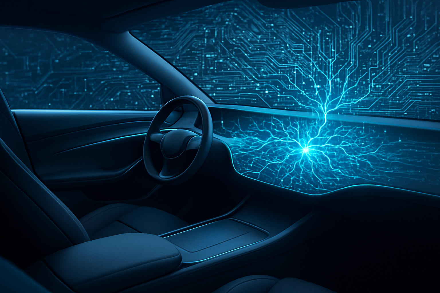
The centerpiece of the agreement is the A16 compute chip, a 1.6-nanometer (nm) class processor designed to handle the massive neural network workloads required for Level 4 autonomous driving. While the "A16" moniker mirrors the nomenclature used by TSMC (NYSE: TSM) for its 1.6nm node, Samsung’s version utilizes its proprietary Gate-All-Around (GAA) transistor architecture and the revolutionary Backside Power Delivery Network (BSPDN). This technology moves power routing to the back of the silicon wafer, drastically reducing voltage drop and allowing for a 20% increase in power efficiency—a critical metric for electric vehicles (EVs) where every watt of compute power consumed is a watt taken away from driving range.
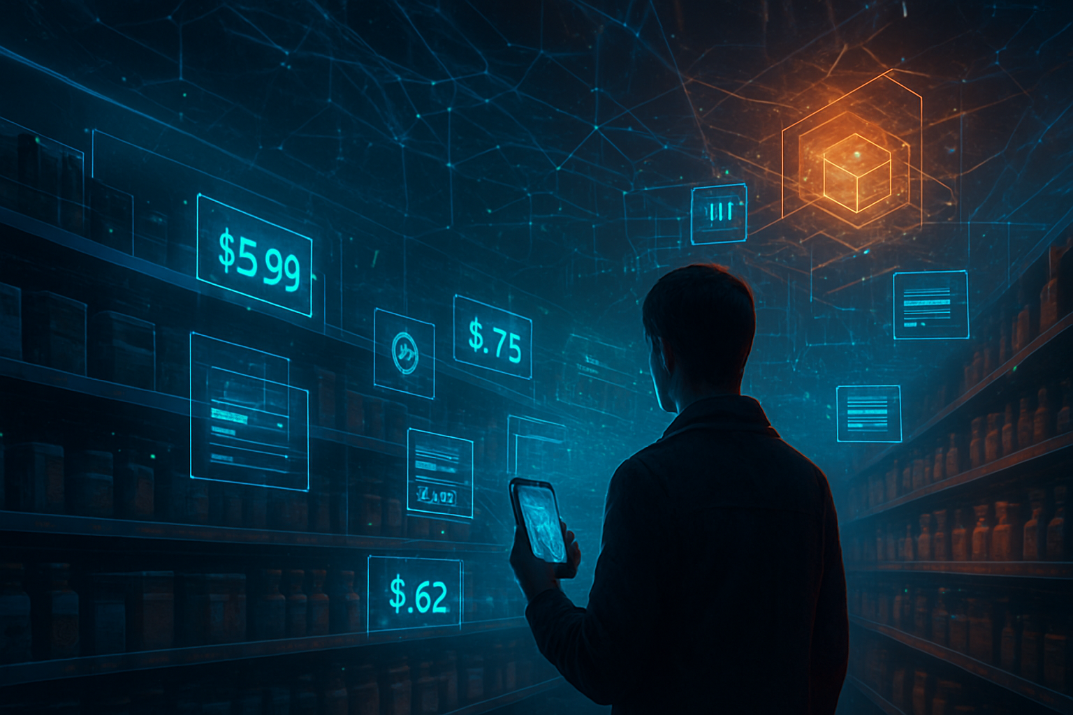
Technically, the A16 is expected to deliver between 1,500 and 2,000 Tera Operations Per Second (TOPS), a nearly tenfold increase over the hardware found in vehicles just three years ago. This massive compute overhead is necessary to process simultaneous data streams from 12+ high-resolution cameras, LiDAR, and radar, while running real-time "world model" simulations that predict the movements of pedestrians and other vehicles. Unlike previous generations that relied on general-purpose GPUs, the A16 features dedicated AI accelerators specifically optimized for Tesla’s FSD (Full Self-Driving) neural networks.
Initial reactions from the AI research community have been overwhelmingly positive, with experts noting that the move to 1.6nm silicon is the only viable path to achieving Level 4 autonomy within a reasonable thermal envelope. "We are seeing the end of the 'brute force' era of automotive AI," said Dr. Aris Thorne, a senior semiconductor analyst. "By integrating BSPDN and moving to the Angstrom era, Tesla and Samsung are solving the 'range killer' problem, where autonomous systems previously drained up to 25% of a vehicle's battery just to stay 'awake'."
A Seismic Shift in the Competitive Landscape
This $16.5 billion deal reshapes the competitive dynamics between tech giants and traditional automakers. By securing a massive portion of Samsung’s 1.6nm capacity at its new Taylor, Texas facility, Tesla has effectively built a "silicon moat" around its autonomous driving lead. This puts immense pressure on rivals like NVIDIA (NASDAQ: NVDA) and Qualcomm (NASDAQ: QCOM), who are also vying for dominance in the high-performance automotive SoC (System-on-Chip) market. While NVIDIA’s Thor platform remains a formidable competitor, Tesla’s vertical integration—designing its own silicon and securing dedicated foundry lines—gives it a significant cost and optimization advantage.
For Samsung, this deal is a monumental victory for its foundry business. After years of trailing TSMC in market share, securing the world’s most advanced automotive AI contract validates Samsung’s aggressive roadmap in GAA and BSPDN technologies. The deal also benefits from the U.S. CHIPS Act, as the Taylor, Texas fab provides a domestic supply chain that mitigates geopolitical risks associated with semiconductor production in East Asia. This strategic positioning makes Samsung an increasingly attractive partner for other Western automakers looking to decouple their silicon supply chains from potential regional instabilities.
Furthermore, the scale of this investment suggests that the "software-defined vehicle" (SDV) is no longer a buzzword but a financial reality. Companies like Mobileye (NASDAQ: MBLY) and even traditional Tier-1 suppliers are now forced to accelerate their silicon roadmaps or risk becoming obsolete. The market is bifurcating into two camps: those who can design and secure 2nm-and-below silicon, and those who will be forced to buy off-the-shelf solutions at a premium, likely lagging several generations behind in AI performance.
The Wider Significance: Silicon as the New Oil
The explosion of automotive silicon fits into a broader global trend where compute power has become the primary driver of industrial value. Just as oil defined the 20th-century automotive era, silicon and AI models are defining the 21st. The shift toward $100 billion in annual silicon demand by 2029 reflects a fundamental change in how we perceive transportation. The car is becoming a mobile data center, an edge-computing node that contributes to a larger hive-mind of autonomous agents.
However, this transition is not without concerns. The reliance on such advanced, centralized silicon raises questions about cybersecurity and the "right to repair." If a single A16 chip controls every aspect of a vehicle's operation, from steering to braking to infotainment, the potential impact of a hardware failure or a sophisticated cyberattack is catastrophic. Moreover, the environmental impact of manufacturing 1.6nm chips—a process that is incredibly energy and water-intensive—must be balanced against the efficiency gains these chips provide to the EVs they power.
Comparisons are already being drawn to the 2021 semiconductor shortage, which crippled the automotive industry. This $16.5 billion deal is a direct response to those lessons, with Tesla and Samsung opting for long-term, multi-year stability over spot-market volatility. It represents a "de-risking" of the AI revolution, ensuring that the hardware necessary for the next decade of innovation is secured today.
The Horizon: From Robotaxis to Humanoid Robots
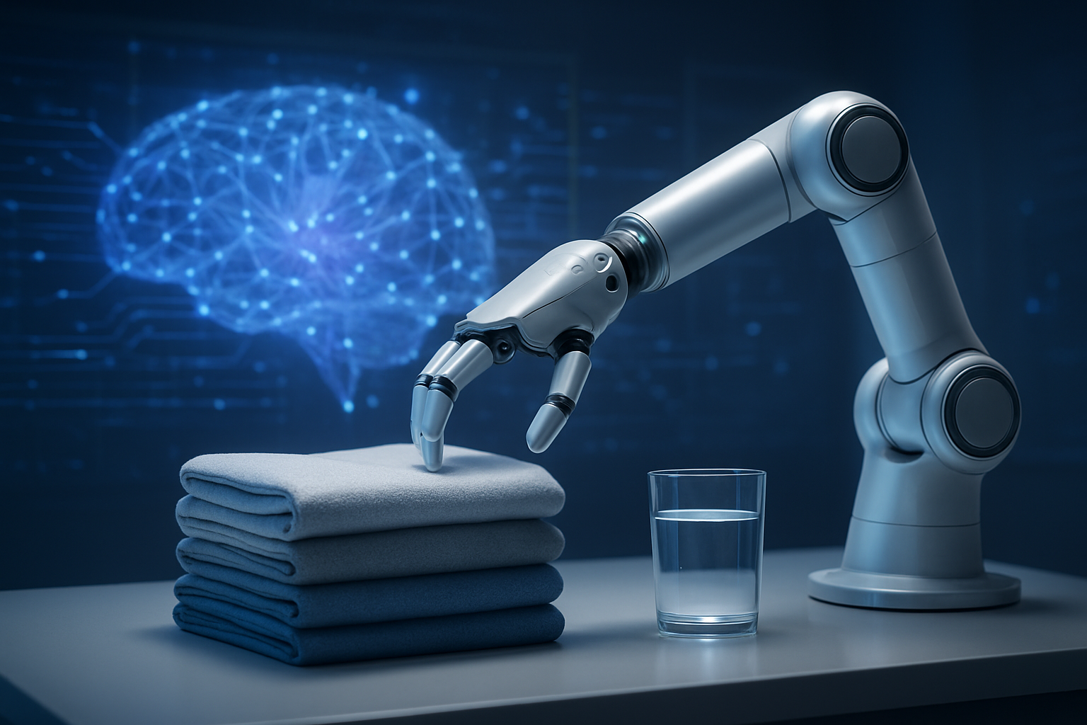
Looking forward, the A16 chip is not just about cars. Elon Musk has hinted that the architecture developed for the A16 will be foundational for the next generation of the Optimus humanoid robot. The requirements for a robot—low power, high-performance inference, and real-time spatial awareness—are nearly identical to those of a self-driving car. We are likely to see a convergence of automotive and robotic silicon, where a single chip architecture powers everything from a long-haul semi-truck to a household assistant.
In the near term, the industry will be watching the ramp-up of the Taylor, Texas fab. If Samsung can achieve high yields on its 1.6nm process by late 2026, it could trigger a wave of similar deals from other tech-heavy automakers like Rivian (NASDAQ: RIVN) or even Apple, should their long-rumored vehicle plans resurface. The ultimate goal remains Level 5 autonomy—a vehicle that can drive anywhere under any conditions—and while the A16 is a massive step forward, the software challenges of "edge case" reasoning remain a significant hurdle that even the most powerful silicon cannot solve alone.
A New Chapter in Automotive History
The Tesla-Samsung deal is more than just a supply agreement; it is a declaration of the new world order in the automotive industry. The key takeaways are clear: the value of a vehicle is shifting from its physical chassis to its digital brain, and the ability to secure leading-edge silicon is now a matter of survival. As we head into 2026, the $16.5 billion committed to the A16 chip serves as a benchmark for the scale of investment required to compete in the age of AI.
This development will likely be remembered as the moment the "computer on wheels" concept became a multi-billion dollar industrial reality. In the coming weeks and months, all eyes will be on the technical benchmarks of the first A16 prototypes and the progress of the Taylor fab. The race for the 1.6nm era has begun, and the stakes for the global economy could not be higher.
This content is intended for informational purposes only and represents analysis of current AI developments.
TokenRing AI delivers enterprise-grade solutions for multi-agent AI workflow orchestration, AI-powered development tools, and seamless remote collaboration platforms.
For more information, visit https://www.tokenring.ai/.