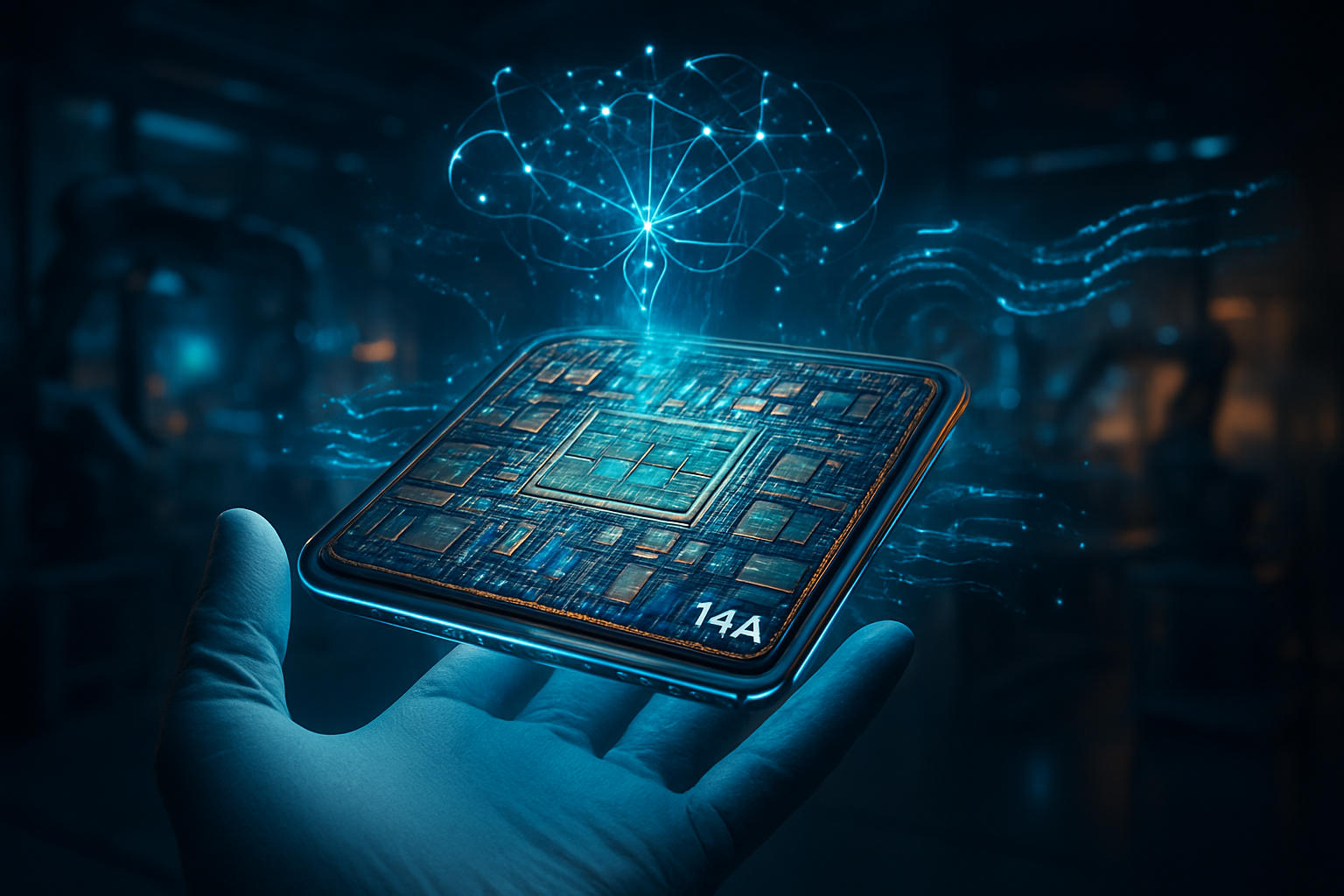
As the world rings in 2026, the global semiconductor landscape has undergone a seismic shift that few predicted a decade ago. RISC-V, the open-source, royalty-free instruction set architecture (ISA), has officially reached a historic 25% global market penetration. What began as an academic project at UC Berkeley is now the "third pillar" of computing, standing alongside the long-dominant x86 and ARM architectures. This milestone, confirmed by industry analysts on January 1, 2026, marks the end of the proprietary duopoly and the beginning of an era defined by "semiconductor sovereignty."
The immediate significance of this development cannot be overstated. Driven by a perfect storm of generative AI demands, geopolitical trade tensions, and a collective industry push for "ARM-free" silicon, RISC-V has evolved from a niche controller architecture into a powerhouse for data centers and AI PCs. With the RISC-V International foundation headquartered in neutral Switzerland, the architecture has become the primary vehicle for nations and corporations to bypass unilateral export controls, effectively decoupling the future of global innovation from the shifting sands of international trade policy.
High-Performance Hardware: Closing the Gap
The technical ascent of RISC-V in the last twelve months has been characterized by a move into high-performance, "server-grade" territory. A standout achievement is the launch of the Alibaba (NYSE: BABA) T-Head XuanTie C930, a 64-bit multi-core processor that features a 16-stage pipeline and performance metrics that rival mid-range server CPUs. Unlike previous iterations that were relegated to low-power IoT devices, the C930 is designed for the heavy lifting of cloud computing and complex AI inference.
At the heart of this technical revolution is the modularity of the RISC-V ISA. While Intel (NASDAQ: INTC) and ARM Holdings (NASDAQ: ARM) offer fixed, "black box" instruction sets, RISC-V allows engineers to add custom extensions specifically for AI workloads. This month, the RISC-V community is finalizing the Vector-Matrix Extension (VME), a critical update that introduces "outer product" formulations for matrix multiplication. This allows for high-throughput AI inference with significantly lower power draw than traditional designs, mimicking the matrix acceleration found in proprietary chips like Apple’s AMX or ARM’s SME.
The hardware ecosystem is also seeing its first "AI PC" breakthroughs. At the upcoming CES 2026, DeepComputing is showcasing the second batch of the DC-ROMA RISC-V Mainboard II for the Framework Laptop 13. Powered by the ESWIN EIC7702X SoC and SiFive P550 cores, this system delivers an aggregate 50 TOPS (Trillion Operations Per Second) of AI performance. This marks the first time a RISC-V consumer device has achieved "near-parity" with mainstream ARM-based laptops, signaling that the software gap—long the Achilles' heel of the architecture—is finally closing.
Corporate Realignment: The "ARM-Free" Movement
The rise of RISC-V has sent shockwaves through the boardrooms of established tech giants. Qualcomm (NASDAQ: QCOM) recently completed a landmark $2.4 billion acquisition of Ventana Micro Systems, a move designed to integrate high-performance RISC-V cores into its "Oryon" CPU line. This strategic pivot provides Qualcomm with an "ARM-free" path for its automotive and enterprise server products, reducing its reliance on costly licensing fees and mitigating the risks of ongoing legal disputes over proprietary ISA rights.
Hyperscalers are also jumping into the fray to gain total control over their silicon destiny. Meta Platforms (NASDAQ: META) recently acquired the RISC-V startup Rivos, allowing the social media giant to "right-size" its compute cores specifically for its Llama-class large language models (LLMs). By optimizing the silicon for the specific math of their own AI models, Meta can achieve performance-per-watt gains that are impossible on off-the-shelf hardware from NVIDIA (NASDAQ: NVDA) or Intel.
The competitive implications are particularly dire for the x86/ARM duopoly. While Intel and AMD (NASDAQ: AMD) still control the majority of the legacy server market, their combined 95% share is under active erosion. The RISC-V Software Ecosystem (RISE) project—a collaborative effort including Alphabet/Google (NASDAQ: GOOGL), Intel, and NVIDIA—has successfully brought Android and major Linux distributions to "Tier-1" status on RISC-V. This ensures that the next generation of cloud and mobile applications can be deployed seamlessly across any architecture, stripping away the "software moat" that previously protected the incumbents.
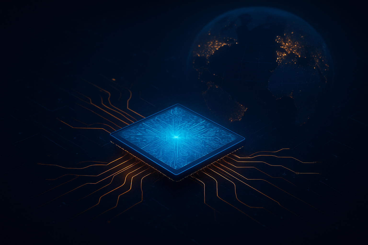
Geopolitical Strategy and Sovereign Silicon
Beyond the technical and corporate battles, the rise of RISC-V is a defining chapter in the "Silicon Cold War." China has adopted RISC-V as a strategic response to U.S. trade restrictions, with the Chinese government mandating its integration into critical infrastructure such as finance, energy, and telecommunications. By late 2025, China accounted for nearly 50% of global RISC-V shipments, building a resilient, indigenous tech stack that is effectively immune to Western export bans.
This movement toward "Sovereign Silicon" is not limited to China. The European Union’s "Digital Autonomy with RISC-V in Europe" (DARE) initiative has already produced the "Titania" AI unit for industrial robotics, reflecting a broader global desire to reduce dependency on U.S.-controlled technology. This trend mirrors the earlier rise of open-source software like Linux; just as Linux broke the proprietary OS monopoly, RISC-V is breaking the proprietary hardware monopoly.
However, this rapid diffusion of high-performance computing power has raised concerns in Washington. The U.S. government’s "AI Diffusion Rule," finalized in early 2025, attempted to tighten controls on AI hardware, but the open-source nature of RISC-V makes it notoriously difficult to regulate. Unlike a physical product, an instruction set is information, and the RISC-V International’s move to Switzerland has successfully shielded the standard from being used as a tool of unilateral economic statecraft.
The Horizon: From Data Centers to Pockets
Looking ahead, the next 24 months will likely see RISC-V move from the data center and the developer's desk into the pockets of everyday consumers. Analysts predict that the first commercial RISC-V smartphones will hit the market by late 2026, supported by the now-mature Android-on-RISC-V ecosystem. Furthermore, the push into the "AI PC" space is expected to accelerate, with Tenstorrent—led by legendary chip architect Jim Keller—preparing its "Ascalon-X" cores to challenge high-end ARM Neoverse designs.
The primary challenge remaining is the optimization of "legacy" software. While new AI and cloud-native applications run beautifully on RISC-V, decades of x86-specific code in the enterprise world will take time to migrate. We can expect to see a surge in AI-powered binary translation tools—similar to Apple's Rosetta 2—that will allow RISC-V systems to run old software with minimal performance hits, further lowering the barrier to adoption.
A New Era of Open Innovation
The 25% market share milestone reached on January 1, 2026, is more than just a statistic; it is a declaration of independence for the global semiconductor industry. RISC-V has proven that an open-source model can foster innovation at a pace that proprietary systems cannot match, particularly in the rapidly evolving field of AI. The architecture has successfully transitioned from a "low-cost alternative" to a "high-performance necessity."
As we move further into 2026, the industry will be watching the upcoming CES announcements and the first wave of RVA23-compliant hardware. The long-term impact is clear: the era of the "instruction set as a product" is over. In its place is a collaborative, global standard that empowers every nation and company to build the specific silicon they need for the AI-driven future. The "Third Pillar" is no longer just standing; it is supporting the weight of the next digital revolution.
This content is intended for informational purposes only and represents analysis of current AI developments.
TokenRing AI delivers enterprise-grade solutions for multi-agent AI workflow orchestration, AI-powered development tools, and seamless remote collaboration platforms.
For more information, visit https://www.tokenring.ai/.