In the rapidly evolving landscape of artificial intelligence, few moments have carried as much weight as the release of Meta’s Llama 3.1 405B. Launched in July 2024, this frontier-level model represented a seismic shift in the industry, marking the first time an open-weight model achieved true parity with the most advanced proprietary systems like GPT-4o. By providing the global developer community with a model of this scale and capability, Meta Platforms, Inc. (NASDAQ:META) effectively democratized high-level AI, allowing organizations to run "God-mode" intelligence on their own private infrastructure without the need for restrictive and expensive API calls.
As we look back from the vantage point of late 2025, the significance of Llama 3.1 405B has only grown. It didn't just provide a powerful tool; it shifted the gravity of AI development away from a handful of "walled gardens" toward a collaborative, open ecosystem. This move forced a radical reassessment of business models across Silicon Valley, proving that the "Linux of AI" was not just a theoretical ambition of Mark Zuckerberg, but a functional reality that has redefined how enterprise-grade AI is deployed globally.
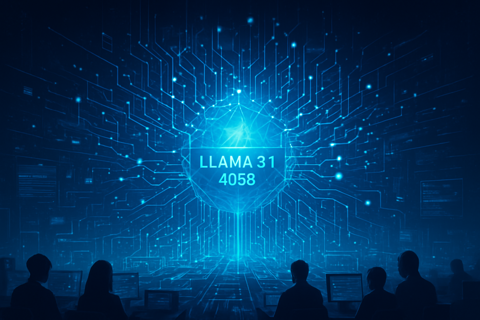
The Technical Titan: Parity at 405 Billion Parameters
The technical specifications of Llama 3.1 405B were, at the time of its release, staggering. Built on a dense transformer architecture with 405 billion parameters, the model was trained on a massive corpus of 15.6 trillion tokens. To achieve this, Meta utilized a custom-built cluster of 16,000 NVIDIA Corporation (NASDAQ:NVDA) H100 GPUs, a feat of engineering that cost an estimated $500 million in compute alone. This massive scale allowed the model to compete head-to-head with GPT-4o from OpenAI and Claude 3.5 Sonnet from Anthropic, consistently hitting benchmarks in the high 80s for MMLU (Massive Multitask Language Understanding) and exceeding 96% on GSM8K mathematical reasoning tests.
One of the most critical technical advancements was the expansion of the context window to 128,000 tokens. This 16-fold increase over the previous Llama 3 iteration enabled developers to process entire books, massive codebases, and complex legal documents in a single prompt. Furthermore, Meta’s "compute-optimal" training strategy focused heavily on synthetic data generation. The 405B model acted as a "teacher," generating millions of high-quality examples to refine smaller, more efficient models like the 8B and 70B versions. This "distillation" process became a industry standard, allowing startups to build specialized, lightweight models that inherited the reasoning capabilities of the 405B giant.
The initial reaction from the AI research community was one of cautious disbelief followed by rapid adoption. For the first time, researchers could peer "under the hood" of a GPT-4 class model. This transparency allowed for unprecedented safety auditing and fine-tuning, which was previously impossible with closed-source APIs. Industry experts noted that while Claude 3.5 Sonnet might have held a slight edge in "graduate-level" reasoning (GPQA), the sheer accessibility and customizability of Llama 3.1 made it the preferred choice for developers who prioritized data sovereignty and cost-efficiency.
Disrupting the Walled Gardens: A Strategic Masterstroke
The release of Llama 3.1 405B sent shockwaves through the competitive landscape, directly challenging the business models of Microsoft Corporation (NASDAQ:MSFT) and Alphabet Inc. (NASDAQ:GOOGL). By offering a frontier model for free download, Meta effectively commoditized the underlying intelligence that OpenAI and Google were trying to sell. This forced proprietary providers to slash their API pricing and accelerate their release cycles. For startups and mid-sized enterprises, the impact was immediate: the cost of running high-level AI dropped by an estimated 50% for those willing to manage their own infrastructure on cloud providers like Amazon.com, Inc. (NASDAQ:AMZN) or on-premise hardware.
Meta’s strategy was clear: by becoming the "foundation" of the AI world, they ensured that the future of the technology would not be gatekept by their rivals. If every developer is building on Llama, Meta controls the standards, the safety protocols, and the developer mindshare. This move also benefited hardware providers like NVIDIA, as the demand for H100 and B200 chips surged among companies eager to host their own Llama instances. The "Llama effect" essentially created a massive secondary market for AI optimization, fine-tuning services, and private cloud hosting, shifting the power dynamic away from centralized AI labs toward the broader tech ecosystem.
However, the disruption wasn't without its casualties. Smaller AI labs that were attempting to build proprietary models just slightly behind the frontier found their "moats" evaporated overnight. Why pay for a mid-tier proprietary model when you can run a frontier-level Llama model for the cost of compute? This led to a wave of consolidation in the industry, as companies shifted their focus from building foundational models to building specialized "agentic" applications on top of the Llama backbone.
Sovereignty and the New AI Landscape
Beyond the balance sheets, Llama 3.1 405B ignited a global conversation about "AI Sovereignty." For the first time, nations and organizations could deploy world-class intelligence without sending their sensitive data to servers in San Francisco or Seattle. This was particularly significant for the public sector, healthcare, and defense industries, where data privacy is paramount. The ability to run Llama 3.1 in air-gapped environments meant that the benefits of the AI revolution could finally reach the most regulated sectors of society.
This democratization also leveled the playing field for international developers. By late 2025, we have seen an explosion of "localized" versions of Llama, fine-tuned for specific languages and cultural contexts that were often overlooked by Western-centric closed models. However, this openness also brought concerns. The "dual-use" nature of such a powerful model meant that bad actors could theoretically fine-tune it for malicious purposes, such as generating biological threats or sophisticated cyberattacks. Meta countered this by releasing a suite of safety tools, including Llama Guard 3 and Prompt Guard, but the debate over the risks of open-weight frontier models remains a central pillar of AI policy discussions today.
The Llama 3.1 release is now viewed as the "Linux moment" for AI. Just as the open-source operating system became the backbone of the internet, Llama has become the backbone of the "Intelligence Age." It proved that the open-source model could not only keep up with the billionaire-funded labs but could actually lead the way in setting industry standards for transparency and accessibility.
The Road to Llama 4 and Beyond
Looking toward the future, the momentum generated by Llama 3.1 has led directly to the recent breakthroughs we are seeing in late 2025. The release of the Llama 4 family earlier this year, including the "Scout" (17B) and "Maverick" (400B MoE) models, has pushed the boundaries even further. Llama 4 Scout, in particular, introduced a 10-million token context window, making "infinite context" a reality for the average developer. This has opened the door for autonomous AI agents that can "remember" years of interaction and manage entire corporate workflows without human intervention.
However, the industry is currently buzzing with rumors of a strategic pivot at Meta. Reports of "Project Avocado" suggest that Meta may be developing its first truly closed-source, high-monetization model to recoup the massive capital expenditures—now exceeding $60 billion—spent on AI infrastructure. This potential shift highlights the central challenge of the open-source movement: the astronomical cost of staying at the absolute frontier. While Llama 3.1 democratized GPT-4 level intelligence, the race for "Artificial General Intelligence" (AGI) may eventually require a return to proprietary models to sustain the necessary investment.
Experts predict that the next 12 months will be defined by "agentic orchestration." Now that high-level reasoning is a commodity, the value has shifted to how these models interact with the physical world and other software systems. The challenges ahead are no longer just about parameter counts, but about reliability, tool-use precision, and the ethical implications of autonomous decision-making.
A Legacy of Openness
In summary, Meta’s Llama 3.1 405B was the catalyst that ended the era of "AI gatekeeping." By achieving parity with the world's most advanced closed models and releasing the weights to the public, Meta fundamentally changed the trajectory of the 21st century’s most important technology. It empowered millions of developers, provided a path for enterprise data sovereignty, and forced a level of transparency that has made AI safer and more robust for everyone.
As we move into 2026, the legacy of Llama 3.1 is visible in every corner of the tech industry—from the smallest startups running 8B models on local laptops to the largest enterprises orchestrating global fleets of 405B-powered agents. While the debate between open and closed models will continue to rage, the "Llama moment" proved once and for all that when you give the world’s developers the best tools, the pace of innovation becomes unstoppable. The coming months will likely see even more specialized applications of this technology, as the world moves from simply "talking" to AI to letting AI "do" the work.
This content is intended for informational purposes only and represents analysis of current AI developments.
TokenRing AI delivers enterprise-grade solutions for multi-agent AI workflow orchestration, AI-powered development tools, and seamless remote collaboration platforms.
For more information, visit https://www.tokenring.ai/.