Tag: AI

  • The “Operating System of Life”: How AlphaFold 3 Redefined Biology and the Drug Discovery Frontier

    The “Operating System of Life”: How AlphaFold 3 Redefined Biology and the Drug Discovery Frontier

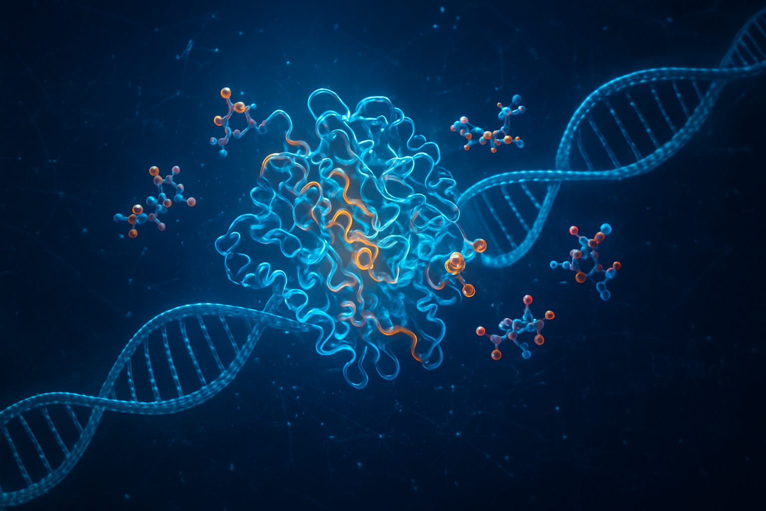
    As of late 2025, the landscape of biological research has undergone a transformation comparable to the digital revolution of the late 20th century. At the center of this shift is AlphaFold 3, the latest iteration of the Nobel Prize-winning artificial intelligence system from Google DeepMind, a subsidiary of Alphabet Inc. (NASDAQ: GOOGL). While its predecessor, AlphaFold 2, solved the 50-year-old "protein folding problem," AlphaFold 3 has gone significantly further, acting as a universal molecular predictor capable of modeling the complex interactions between proteins, DNA, RNA, ligands, and ions.

    The immediate significance of AlphaFold 3 lies in its transition from a specialized scientific tool to a foundational "operating system" for drug discovery. By providing a high-fidelity 3D map of how life’s molecules interact, the model has effectively reduced the time required for initial drug target identification from years to mere minutes. This leap in capability has not only accelerated academic research but has also sparked a multi-billion dollar "arms race" among pharmaceutical giants and AI-native biotech startups, fundamentally altering the economics of the healthcare industry.

    From Evoformer to Diffusion: The Technical Leap

    Technically, AlphaFold 3 represents a radical departure from the architecture of its predecessors. While AlphaFold 2 relied on the "Evoformer" module to process Multiple Sequence Alignments (MSAs), AlphaFold 3 utilizes a generative Diffusion-based architecture—the same underlying technology found in AI image generators like Stable Diffusion. This shift allows the model to predict raw atomic coordinates directly, bypassing the need for rigid chemical bonding rules. The result is a system that can model over 99% of the molecular types documented in the Protein Data Bank, including complex heteromeric assemblies that were previously impossible to predict with accuracy.

    A key advancement is the introduction of the Pairformer, which replaced the MSA-heavy Evoformer. By focusing on pairwise representations—how every atom in a complex relates to every other—the model has become significantly more data-efficient. In benchmarks conducted throughout 2024 and 2025, AlphaFold 3 demonstrated a 50% improvement in accuracy for ligand-binding predictions compared to traditional physics-based docking tools. This capability is critical for drug discovery, as it allows researchers to see exactly how a potential drug molecule (a ligand) will nestle into the pocket of a target protein.

    The initial reaction from the AI research community was a mixture of awe and friction. In mid-2024, Google DeepMind faced intense criticism for publishing the research without releasing the model’s code, leading to an open letter signed by over 1,000 scientists. However, by November 2024, the company pivoted, releasing the full model code and weights for academic use. This move solidified AlphaFold 3 as the "Gold Standard" in structural biology, though it also paved the way for community-driven competitors like Boltz-1 and OpenFold 3 to emerge in late 2025, offering commercially unrestricted alternatives.

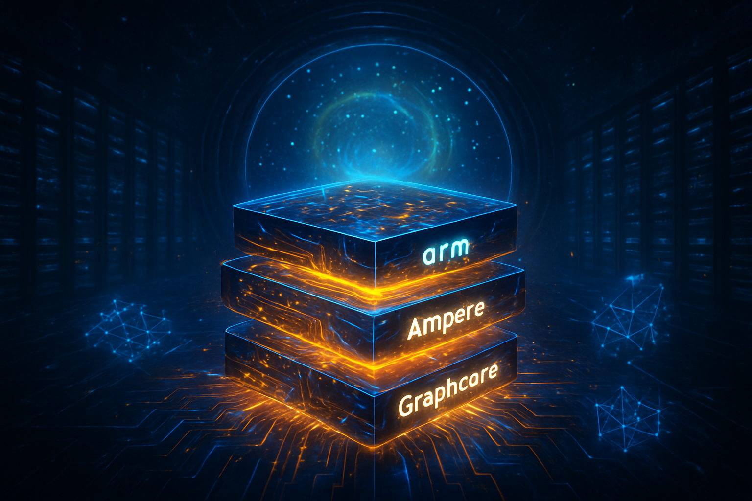
    The Commercial Arms Race: Isomorphic Labs and the "Big Pharma" Pivot

    The commercialization of AlphaFold 3 is spearheaded by Isomorphic Labs, another Alphabet subsidiary led by DeepMind co-founder Sir Demis Hassabis. By late 2025, Isomorphic has established itself as a "bellwether" for the TechBio sector. The company secured landmark partnerships with Eli Lilly (NYSE: LLY) and Novartis (NYSE: NVS), worth a combined potential value of nearly $3 billion in milestones. These collaborations have already moved beyond theoretical research, with Isomorphic confirming in early 2025 that several internal drug candidates in oncology and immunology are nearing Phase I clinical trials.

    The competitive landscape has reacted with unprecedented speed. NVIDIA (NASDAQ: NVDA) has positioned its BioNeMo platform as the central infrastructure for the industry, hosting a variety of models including AlphaFold 3 and its rivals. Meanwhile, startups like EvolutionaryScale, founded by former Meta Platforms (NASDAQ: META) researchers, have launched models like ESM3, which focus on generating entirely new proteins rather than just predicting existing ones. This has shifted the market moat: while structure prediction has become commoditized, the real competitive advantage now lies in proprietary datasets and the ability to conduct rapid "wet-lab" validation.

    The impact on market positioning is clear. Major pharmaceutical companies are no longer just "using" AI; they are rebuilding their entire R&D pipelines around it. Eli Lilly, for instance, is expected to launch a dedicated "AI Factory" in early 2026 in collaboration with NVIDIA, intended to automate the synthesis and testing of molecules designed by AlphaFold-like systems. This "Grand Convergence" of AI and robotics is expected to reduce the average cost of bringing a drug to market by 25% to 45% by the end of the decade.

    Broader Significance: From Blueprints to Biosecurity

    In the broader context of AI history, AlphaFold 3 is frequently compared to the Human Genome Project (HGP). If the HGP provided the "static blueprint" of life, AlphaFold 3 provides the "operational manual." It allows scientists to see how the biological machines coded by our DNA actually function and interact. Unlike Large Language Models (LLMs) like ChatGPT, which predict the next word in a sequence, AlphaFold 3 predicts physical reality, making it a primary engine for tangible economic and medical value.

    However, this power has raised significant ethical and security concerns. A landmark study in late 2025 highlighted the risk of "toxin paraphrasing," where AI models could be used to design synthetic variants of dangerous toxins—such as ricin—that remain functional but are invisible to current biosecurity screening software. This has led to a July 2025 U.S. government AI Action Plan focusing on dual-use risks in biology, prompting calls for a dedicated federal agency to oversee AI-facilitated biosecurity and more stringent screening for commercial DNA synthesis.

    Despite these concerns, the "Open Science" debate has largely resolved in favor of transparency. The 2024 Nobel Prize in Chemistry, awarded to Demis Hassabis and John Jumper for their work on AlphaFold, served as a "halo effect" for the industry, stabilizing venture capital confidence during a period of broader market volatility. The consensus in late 2025 is that AlphaFold 3 has successfully moved biology from a descriptive science to a predictive and programmable one.

    The Road Ahead: 4D Biology and Self-Driving Labs

    Looking toward 2026, the focus of the research community is shifting from "static snapshots" to "conformational dynamics." While AlphaFold 3 provides a 3D picture of a molecule, the next frontier is the "4D movie"—predicting how proteins move, vibrate, and change shape in response to their environment. This is crucial for targeting "undruggable" proteins that only reveal binding pockets during specific movements. Experts predict that the integration of AlphaFold 3 with physics-based molecular dynamics will be the dominant research trend of the coming year.

    Another major development on the horizon is the proliferation of Autonomous "Self-Driving" Labs (SDLs). Companies like Insilico Medicine and Recursion Pharmaceuticals are already utilizing closed-loop systems where AI designs a molecule, a robot builds and tests it, and the results are fed back into the AI to refine the next design. These labs operate 24/7, potentially increasing experimental R&D speeds by up to 100x. The industry is closely watching the first "AI-native" drug candidates, which are expected to yield critical Phase II and III trial data throughout 2026.

    The challenges remain significant, particularly regarding the "Ion Problem"—where AI occasionally misplaces ions in molecular models—and the ongoing need for experimental verification via methods like Cryo-Electron Microscopy. Nevertheless, the trajectory is clear: the first FDA approval for a drug designed from the ground up by AI is widely expected by late 2026 or 2027.

    A New Era for Human Health

    The emergence of AlphaFold 3 marks a definitive turning point in the history of science. By bridging the gap between genomic information and biological function, Google DeepMind has provided humanity with a tool of unprecedented precision. The key takeaways from the 2024–2025 period are the democratization of high-tier structural biology through open-source models and the rapid commercialization of AI-designed molecules by Isomorphic Labs and its partners.

    As we move into 2026, the industry's eyes will be on the J.P. Morgan Healthcare Conference in January, where major updates on AI-driven pipelines are expected. The transition from "discovery" to "design" is no longer a futuristic concept; it is the current reality of the pharmaceutical industry. While the risks of dual-use technology must be managed with extreme care, the potential for AlphaFold 3 to address previously incurable diseases and accelerate our understanding of life itself remains the most compelling story in modern technology.


    This content is intended for informational purposes only and represents analysis of current AI developments.

    TokenRing AI delivers enterprise-grade solutions for multi-agent AI workflow orchestration, AI-powered development tools, and seamless remote collaboration platforms.
    For more information, visit https://www.tokenring.ai/.

  • The Great Memory Pivot: HBM4 and the 3D Stacking Revolution of 2026

    The Great Memory Pivot: HBM4 and the 3D Stacking Revolution of 2026

    As 2025 draws to a close, the semiconductor industry is standing at the precipice of its most significant architectural shift in a decade. The transition to High Bandwidth Memory 4 (HBM4) has moved from theoretical roadmaps to the factory floors of the world’s largest chipmakers. This week, industry leaders confirmed that the first qualification samples of HBM4 are reaching key partners, signaling the end of the HBM3e era and the beginning of a new epoch in AI hardware.

    The stakes could not be higher. As AI models like GPT-5 and its successors push toward the 100-trillion parameter mark, the "memory wall"—the bottleneck where data cannot move fast enough from memory to the processor—has become the primary constraint on AI progress. HBM4, with its radical 2048-bit interface and the nascent implementation of hybrid bonding, is designed to shatter this wall. For the titans of the industry, the race to master this technology by the 2026 product cycle will determine who dominates the next phase of the AI revolution.

    The 2048-Bit Leap: Engineering the Future of Data

    The technical specifications of HBM4 represent a departure from nearly every standard that preceded it. For the first time, the industry is doubling the memory interface width from 1024-bit to 2048-bit. This change allows HBM4 to achieve bandwidths exceeding 2.0 terabytes per second (TB/s) per stack without the punishing power consumption associated with the high clock speeds of HBM3e. By late 2025, SK Hynix (KRX: 000660) and Samsung Electronics (KRX: 005930) have both reported successful pilot runs of 12-layer (12-Hi) HBM4, with 16-layer stacks expected to follow by mid-2026.

    Central to this transition is the move toward "hybrid bonding," a process that replaces traditional micro-bumps with direct copper-to-copper connections. Unlike previous generations that relied on Thermal Compression (TC) bonding, hybrid bonding eliminates the gap between DRAM layers, reducing the total height of the stack and significantly improving thermal conductivity. This is critical because JEDEC, the global standards body, recently set the HBM4 package thickness limit at 775 micrometers (μm). To fit 16 layers into that vertical space, manufacturers must thin DRAM wafers to a staggering 30μm—roughly one-third the thickness of a human hair—creating immense challenges for manufacturing yields.

    The industry reaction has been one of cautious optimism tempered by the sheer complexity of the task. While SK Hynix has leaned on its proven Advanced MR-MUF (Mass Reflow Molded Underfill) technology for its initial 12-layer HBM4, Samsung has taken a more aggressive "leapfrog" approach, aiming to be the first to implement hybrid bonding at scale for 16-layer products. Industry experts note that the move to a 2048-bit interface also requires a fundamental redesign of the logic base die, leading to unprecedented collaborations between memory makers and foundries like TSMC (NYSE: TSM).

    A New Power Dynamic: Foundries and Memory Makers Unite

    The HBM4 era is fundamentally altering the competitive landscape for AI companies. No longer can memory be treated as a commodity; it is now an integral part of the processor's logic. This has led to the formation of "mega-alliances." SK Hynix has solidified a "one-team" partnership with TSMC to manufacture the HBM4 logic base die on 5nm and 12nm nodes. This alliance aims to ensure that SK Hynix memory is perfectly tuned for the upcoming NVIDIA (NASDAQ: NVDA) "Rubin" R100 GPUs, which are expected to be the first major accelerators to utilize HBM4 in 2026.

    Samsung Electronics, meanwhile, is leveraging its unique position as the world’s only "turnkey" provider. By offering memory production, logic die fabrication on its own 4nm process, and advanced 2.5D/3D packaging under one roof, Samsung hopes to capture customers who want to bypass the complex TSMC supply chain. However, in a sign of the market's pragmatism, Samsung also entered a partnership with TSMC in late 2025 to ensure its HBM4 stacks remain compatible with TSMC’s CoWoS (Chip on Wafer on Substrate) packaging, ensuring it doesn't lose out on the massive NVIDIA and AMD (NASDAQ: AMD) contracts.

    For Micron Technology (NASDAQ: MU), the transition is a high-stakes catch-up game. After successfully gaining market share with HBM3e, Micron is currently ramping up its 12-layer HBM4 samples using its 1-beta DRAM process. While reports of yield issues surfaced in the final quarter of 2025, Micron remains a critical third pillar in the supply chain, particularly for North American clients looking to diversify their sourcing away from purely South Korean suppliers.

    Breaking the Memory Wall: Why 3D Stacking Matters

    The broader significance of HBM4 lies in its potential to move from 2.5D packaging to true 3D stacking—placing the memory directly on top of the GPU logic. This "memory-on-logic" architecture is the holy grail of AI hardware, as it reduces the distance data must travel from millimeters to microns. The result is a projected 10% to 15% reduction in latency and a massive 40% to 70% reduction in the energy required to move each bit of data. In an era where AI data centers are consuming gigawatts of power, these efficiency gains are not just beneficial; they are essential for the industry's survival.

    However, this transition introduces the "thermal crosstalk" problem. When memory is stacked directly on a GPU that generates 700W to 1000W of heat, the thermal energy can bleed into the DRAM layers, causing data corruption or requiring aggressive "refresh" cycles that tank performance. Managing this heat is the primary hurdle of late 2025. Engineers are currently experimenting with double-sided liquid cooling and specialized thermal interface materials to "sandwich" the heat between cooling plates.

    This shift mirrors previous milestones like the introduction of the first HBM by AMD in 2015, but at a vastly different scale. If the industry successfully navigates the thermal and yield challenges of HBM4, it will enable the training of models with hundreds of trillions of parameters, moving the needle from "Large Language Models" to "World Models" that can process video, logic, and physical simulations in real-time.

    The Road to 2026: What Lies Ahead

    Looking forward, the first half of 2026 will be defined by the "Battle of the Accelerators." NVIDIA’s Rubin architecture and AMD’s Instinct MI400 series are both designed around the capabilities of HBM4. These chips are expected to offer more than 0.5 TB of memory per GPU, with aggregate bandwidths nearing 20 TB/s. Such specs will allow a single server rack to hold the entire weights of a frontier-class model in active memory, drastically reducing the need for complex, multi-node communication.

    The next major challenge on the horizon is the standardization of "Bufferless HBM." By removing the buffer die entirely and letting the GPU's memory controller manage the DRAM directly, latency could be slashed further. However, this requires an even tighter level of integration between companies that were once competitors. Experts predict that by late 2026, we will see the first "custom HBM" solutions, where companies like Google (NASDAQ: GOOGL) or Amazon (NASDAQ: AMZN) co-design the HBM4 logic die specifically for their internal AI TPUs.

    Summary of a Pivotal Year

    The transition to HBM4 in late 2025 marks the moment when memory stopped being a peripheral component and became the heart of AI compute. The move to a 2048-bit interface and the pilot programs for hybrid bonding represent a massive engineering feat that has pushed the limits of material science and manufacturing precision. As SK Hynix, Samsung, and Micron prepare for mass production in early 2026, the focus has shifted from "can we build it?" to "can we yield it?"

    This development is more than a technical upgrade; it is a strategic realignment of the global semiconductor industry. The partnerships between memory giants and foundries like TSMC have created a new "AI Silicon Alliance" that will define the next decade of computing. As we move into 2026, the success of these HBM4 integrations will be the primary factor in determining the speed and scale of AI's integration into every facet of the global economy.


    This content is intended for informational purposes only and represents analysis of current AI developments.

    TokenRing AI delivers enterprise-grade solutions for multi-agent AI workflow orchestration, AI-powered development tools, and seamless remote collaboration platforms.
    For more information, visit https://www.tokenring.ai/.

  • The Great Decoupling: How RISC-V Became China’s Ultimate Weapon for Semiconductor Sovereignty

    The Great Decoupling: How RISC-V Became China’s Ultimate Weapon for Semiconductor Sovereignty

    As 2025 draws to a close, the global semiconductor landscape has undergone a seismic shift, driven not by a new proprietary breakthrough, but by the rapid ascent of an open-source architecture. RISC-V, the open-standard instruction set architecture (ISA), has officially transitioned from an academic curiosity to a central pillar of geopolitical strategy. In a year defined by escalating trade tensions and tightening export controls, Beijing has aggressively positioned RISC-V as the cornerstone of its "semiconductor sovereignty," aiming to permanently bypass the Western-controlled duopoly of x86 and ARM.

    The significance of this movement cannot be overstated. By leveraging an architecture maintained by a Swiss-based non-profit, RISC-V International, China has found a strategic loophole that is largely immune to unilateral U.S. sanctions. This year’s nationwide push, codified in landmark government guidelines, signals a point of no return: the era of Western dominance over the "brains" of computing is being challenged by a decentralized, open-source insurgency that is now powering everything from IoT sensors to high-performance AI data centers across Asia.

    The Architecture of Autonomy: Technical Breakthroughs in 2025

    The technical momentum behind RISC-V reached a fever pitch in March 2025, when a coalition of eight high-level Chinese government bodies—including the Ministry of Industry and Information Technology (MIIT) and the Cyberspace Administration of China (CAC)—released a comprehensive policy framework. These guidelines mandated the integration of RISC-V into critical infrastructure, including energy, finance, and telecommunications. This was not merely a suggestion; it was a directive to replace systems powered by Intel Corporation (NASDAQ: INTC) and Advanced Micro Devices, Inc. (NASDAQ: AMD) with "indigenous and controllable" silicon.

    At the heart of this technical revolution is Alibaba Group Holding Limited (NYSE: BABA) and its dedicated chip unit, T-Head. In early 2025, Alibaba unveiled the XuanTie C930, the world’s first truly "server-grade" 64-bit multi-core RISC-V processor. Unlike its predecessors, which were relegated to low-power tasks, the C930 features a sophisticated 16-stage pipeline and a 6-decode width, achieving performance metrics that rival mid-range server CPUs. Fully compliant with the RVA23 profile, the C930 includes essential extensions for cloud virtualization and Vector 1.0 for AI workloads, allowing it to handle the complex computations required for modern LLMs.

    This development marks a radical departure from previous years, where RISC-V was often criticized for its fragmented ecosystem. The 2025 guidelines have successfully unified Chinese developers under a single set of standards, preventing the "forking" of the architecture that many experts feared. By standardizing the software stack—from the Linux kernel to AI frameworks like PyTorch—China has created a plug-and-play environment for RISC-V that is now attracting massive investment from both state-backed enterprises and private startups.

    Market Disruption and the Threat to ARM’s Hegemony

    The rise of RISC-V poses an existential threat to the licensing model of Arm Holdings plc (NASDAQ: ARM). For decades, ARM has enjoyed a near-monopoly on mobile and embedded processors, but its proprietary nature and UK/US nexus have made it a liability in the eyes of Chinese firms. By late 2025, RISC-V has achieved a staggering 25% market penetration in China’s specialized AI and IoT sectors. Companies are migrating to the open-source ISA not just to avoid millions in annual licensing fees, but to eliminate the risk of their licenses being revoked due to shifting geopolitical winds.

    Major tech giants are already feeling the heat. While NVIDIA Corporation (NASDAQ: NVDA) remains the king of high-end AI training, the "DeepSeek" catalyst of late 2024 and early 2025 has shown that high-efficiency, low-cost AI models can thrive on alternative hardware. Smaller Chinese firms are increasingly deploying RISC-V AI accelerators that offer a 30–50% cost reduction compared to sanctioned Western hardware. While these chips may not match the raw performance of an H100, their "good enough" performance at a fraction of the cost is disrupting the mid-market and edge-computing sectors.

    Furthermore, the impact extends beyond China. India has emerged as a formidable second front in the RISC-V revolution. Under the Digital India RISC-V (DIR-V) program, India launched the DHRUV64 in December 2025, its first homegrown 1.0 GHz dual-core processor. By positioning RISC-V as a tool for "Atmanirbhar" (self-reliance), India is creating a parallel ecosystem that mirrors China’s pursuit of sovereignty but remains integrated with global markets. This dual-pronged pressure from the world’s two most populous nations is forcing traditional chipmakers to reconsider their long-term strategies in the Global South.

    Geopolitical Implications and the Quest for Sovereignty

    The broader significance of the RISC-V surge lies in its role as a "sanction-proof" foundation. Because the RISC-V instruction set itself is open-source and managed in Switzerland, the U.S. Department of Commerce cannot "turn off" the architecture. While the manufacturing of these chips—often handled by Taiwan Semiconductor Manufacturing Company (NYSE: TSM) or Samsung—remains a bottleneck subject to export controls, the ability to design and iterate on the core architecture remains firmly in domestic hands.

    This has led to a new era of "Semiconductor Sovereignty." For China, RISC-V is a shield against containment; for India, it is a sword to carve out a niche in the global design market. This shift mirrors previous milestones in open-source history, such as the rise of Linux in the server market, but with much higher stakes. The 2025 guidelines in Beijing represent the first time a major world power has officially designated an open-source hardware standard as a national security priority, effectively treating silicon as a public utility rather than a corporate product.

    However, this transition is not without concerns. Critics argue that China’s aggressive subsidization could lead to a "dumping" of low-cost RISC-V chips on the global market, potentially stifling innovation in other regions. There are also fears that the U.S. might respond with even more stringent "AI Diffusion Rules," potentially targeting the collaborative nature of open-source development itself—a move that would have profound implications for the global research community.

    The Horizon: 7nm Dreams and the Future of Compute

    Looking ahead to 2026 and beyond, the focus will shift from architecture to manufacturing. China is expected to pour even more resources into domestic lithography to ensure that its RISC-V designs can be produced at advanced nodes without relying on Western-aligned foundries. Meanwhile, India has already announced a roadmap for a 7nm RISC-V processor led by IIT Madras, aiming to enter the high-end computing space by 2027.

    In the near term, expect to see RISC-V move from the data center to the desktop. With the 2025 guidelines providing the necessary tailwinds, several Chinese OEMs are rumored to be preparing RISC-V-based laptops for the education and government sectors. The challenge remains the "software gap"—ensuring that mainstream applications run seamlessly on the new architecture. However, with the rapid adoption of cloud-native and browser-based workflows, the underlying ISA is becoming less visible to the end-user, making the transition easier than ever before.

    Experts predict that by 2030, RISC-V could account for as much as 30-40% of the global processor market. The "Swiss model" of neutrality has provided a safe harbor for innovation during a time of intense global friction, and the momentum built in 2025 suggests that the genie is officially out of the bottle.

    A New Chapter in Computing History

    The events of 2025 have solidified RISC-V’s position as the most disruptive force in the semiconductor industry in decades. Beijing’s nationwide push has successfully turned an open-source project into a formidable tool of statecraft, allowing China to build a resilient, indigenous tech stack that is increasingly decoupled from Western control. Alibaba’s XuanTie C930 and India’s DIR-V program are just the first of many milestones in this new era of sovereign silicon.

    As we move into 2026, the key takeaway is that the global chip industry is no longer a monolith. We are witnessing the birth of a multi-polar computing world where open-source standards provide the level playing field that proprietary architectures once dominated. For tech giants, the message is clear: the monopoly on the instruction set is over. For the rest of the world, the rise of RISC-V promises a future of more diverse, accessible, and resilient technology—albeit one shaped by the complex realities of 21st-century geopolitics.

    Watch for the next wave of RISC-V announcements at the upcoming 2026 global summits, where the battle for "silicon supremacy" will likely enter its most intense phase yet.


    This content is intended for informational purposes only and represents analysis of current AI and semiconductor developments.

    TokenRing AI delivers enterprise-grade solutions for multi-agent AI workflow orchestration, AI-powered development tools, and seamless remote collaboration platforms.
    For more information, visit https://www.tokenring.ai/.

  • The Silicon Squeeze: Why Advanced Packaging is the New Gatekeeper of the AI Revolution in 2025

    The Silicon Squeeze: Why Advanced Packaging is the New Gatekeeper of the AI Revolution in 2025

    As of December 30, 2025, the narrative of the global AI race has shifted from a battle over transistor counts to a desperate scramble for "back-end" real estate. For the past decade, the semiconductor industry focused on the front-end—the complex lithography required to etch circuits onto silicon wafers. However, in the closing days of 2025, the industry has hit a physical wall. The primary bottleneck for the world’s most powerful AI chips is no longer the ability to print them, but the ability to package them. Advanced packaging technologies like TSMC’s CoWoS and Intel’s Foveros have become the most precious commodities in the tech world, dictating the pace of progress for every major AI lab from San Francisco to Beijing.

    The significance of this shift cannot be overstated. With lead times for flagship AI accelerators like NVIDIA’s Blackwell architecture stretching to 18 months, the "Silicon Squeeze" has turned advanced packaging into a strategic geopolitical asset. As demand for generative AI and massive language models continues to outpace supply, the ability to "stitch" together multiple silicon dies into a single high-performance module is the only way to bypass the physical limits of traditional chip manufacturing. In 2025, the "chiplet" revolution has officially arrived, and those who control the packaging lines now control the future of artificial intelligence.

    The Technical Wall: Reticle Limits and the Rise of CoWoS-L

    The technical crisis of 2025 stems from a physical constraint known as the "reticle limit." For years, semiconductor manufacturers like Taiwan Semiconductor Manufacturing Co. (NYSE: TSM) could simply make a single chip larger to increase its power. However, standard lithography tools can only expose an area of approximately 858 mm² at once. NVIDIA (NASDAQ: NVDA) reached this limit with its previous generations, but the demands of 2025-era AI require far more silicon than a single exposure can provide. To solve this, the industry has moved toward heterogeneous integration—combining multiple smaller "chiplets" onto a single substrate to act as one giant processor.

    TSMC has maintained its lead through CoWoS-L (Chip on Wafer on Substrate – Local Silicon Interconnect). Unlike previous iterations that used a massive, expensive silicon interposer, CoWoS-L utilizes tiny silicon bridges to link dies with massive bandwidth. This technology is the backbone of the NVIDIA Blackwell (B200) and the upcoming Rubin (R100) architectures. The Rubin chip, entering volume production as 2025 draws to a close, is a marvel of engineering that scales to a "4x reticle" design, effectively stitching together four standard-sized chips into a single super-processor. This complexity, however, comes at a cost: yield rates for these multi-die modules remain volatile, and a single defect in one of the 16 integrated HBM4 (High Bandwidth Memory) stacks can ruin a module worth tens of thousands of dollars.

    The High-Stakes Rivalry: Intel’s $5 Billion Diversification and AMD’s Acceleration

    The packaging bottleneck has forced a radical reshuffling of industry alliances. In one of the most significant strategic pivots of the year, NVIDIA reportedly invested $5 billion into Intel (NASDAQ: INTC) Foundry Services in late 2025. This move was designed to secure capacity for Intel’s Foveros 3D stacking and EMIB (Embedded Multi-die Interconnect Bridge) technologies, providing NVIDIA with a vital "Plan B" to reduce its total reliance on TSMC. Intel’s aggressive expansion of its packaging facilities in Malaysia and Oregon has positioned it as the only viable Western alternative for high-end AI assembly, a goal CEO Pat Gelsinger has pursued relentlessly to revitalize the company’s foundry business.

    Meanwhile, Advanced Micro Devices (NASDAQ: AMD) has accelerated its own roadmap to capitalize on the supply gaps. The AMD Instinct MI350 series, launched in mid-2025, utilizes a sophisticated 3D chiplet architecture that rivals NVIDIA’s Blackwell in memory density. To bypass the TSMC logjam, AMD has turned to "Outsourced Semiconductor Assembly and Test" (OSAT) giants like ASE Technology Holding (NYSE: ASX) and Amkor Technology (NASDAQ: AMKR). These firms are rapidly building out "CoWoS-like" capacity in Arizona and Taiwan, though they too are hampered by 12-month lead times for the specialized equipment required to handle the ultra-fine interconnects of 2025-grade silicon.

    The Wider Significance: Geopolitics and the End of Monolithic Computing

    The shift to advanced packaging represents the end of the "monolithic era" of computing. For fifty years, the industry followed Moore’s Law by shrinking transistors on a single piece of silicon. In 2025, that era is over. The future is modular, and the economic implications are profound. Because advanced packaging is so capital-intensive and requires such high precision, it has created a new "moat" that favors the largest incumbents. Hyperscalers like Meta (NASDAQ: META), Microsoft (NASDAQ: MSFT), and Amazon (NASDAQ: AMZN) are now pre-booking packaging capacity up to two years in advance, a practice that effectively crowds out smaller AI startups and academic researchers.

    This bottleneck also has a massive impact on the global supply chain's resilience. Most advanced packaging still occurs in East Asia, creating a single point of failure that keeps policymakers in Washington and Brussels awake at night. While the U.S. CHIPS Act has funded domestic fabrication plants, the "back-end" packaging remains the missing link. In late 2025, we are seeing the first real efforts to "reshore" this capability, with new facilities in the American Southwest beginning to come online. However, the transition is slow; the expertise required for 2.5D and 3D integration is highly specialized, and the labor market for packaging engineers is currently the tightest in the tech sector.

    The Next Frontier: Glass Substrates and Panel-Level Packaging

    Looking toward 2026 and 2027, the industry is already searching for the next breakthrough to break the current bottleneck. The most promising development is the transition to glass substrates. Traditional organic substrates are prone to warping and heat-related issues as chips get larger and hotter. Glass offers superior flatness and thermal stability, allowing for even denser interconnects. Intel is currently leading the charge in glass substrate research, with plans to integrate the technology into its 2026 product lines. If successful, glass could allow for "system-in-package" designs that are significantly larger than anything possible today.

    Furthermore, the industry is eyeing Panel-Level Packaging (PLP). Currently, chips are packaged on circular 300mm wafers, which results in significant wasted space at the edges. PLP uses large rectangular panels—similar to those used in the display industry—to process hundreds of chips at once. This could potentially increase throughput by 3x to 4x, finally easing the supply constraints that have defined 2025. However, the transition to PLP requires an entirely new ecosystem of equipment and materials, meaning it is unlikely to provide relief for the current Blackwell and MI350 backlogs until at least late 2026.

    Summary of the 2025 Silicon Landscape

    As 2025 draws to a close, the semiconductor industry has successfully navigated the challenges of sub-3nm fabrication, only to find itself trapped by the physical limits of how those chips are put together. The "Silicon Squeeze" has made advanced packaging the ultimate arbiter of AI power. NVIDIA’s 18-month lead times and the strategic move toward Intel’s packaging lines underscore a new reality: in the AI era, it’s not just about what you can build on the silicon, but how much silicon you can link together.

    The coming months will be defined by how quickly TSMC, Intel, and Samsung (KRX: 005930) can scale their 3D stacking capacities. For investors and tech leaders, the metrics to watch are no longer just wafer starts, but "packaging out-turns" and "interposer yields." As we head into 2026, the companies that master the art of the chiplet will be the ones that define the next plateau of artificial intelligence. The revolution is no longer just in the code—it’s in the package.


    This content is intended for informational purposes only and represents analysis of current AI developments.

    TokenRing AI delivers enterprise-grade solutions for multi-agent AI workflow orchestration, AI-powered development tools, and seamless remote collaboration platforms.
    For more information, visit https://www.tokenring.ai/.

  • The Great Decoupling: How Hyperscaler Silicon Is Redrawing the AI Power Map in 2025

    The Great Decoupling: How Hyperscaler Silicon Is Redrawing the AI Power Map in 2025

    As of late 2025, the artificial intelligence industry has reached a pivotal inflection point: the era of "Silicon Sovereignty." For years, the world’s largest cloud providers were beholden to a single gatekeeper for the compute power necessary to fuel the generative AI revolution. Today, that dynamic has fundamentally shifted. Microsoft, Amazon, and Google have successfully transitioned from being NVIDIA's largest customers to becoming its most formidable architectural competitors, deploying a new generation of custom-designed Application-Specific Integrated Circuits (ASICs) that are now handling a massive portion of the world's AI workloads.

    This strategic pivot is not merely about cost-cutting; it is about vertical integration. By designing chips like the Maia 200, Trainium 3, and TPU v7 (Ironwood) specifically for their own proprietary models—such as GPT-4, Claude, and Gemini—these hyperscalers are achieving performance-per-watt efficiencies that general-purpose hardware cannot match. This "great decoupling" has seen internal silicon capture a projected 15-20% of the total AI accelerator market share this year, signaling a permanent end to the era of hardware monoculture in the data center.

    The Technical Vanguard: Maia, Trainium, and Ironwood

    The technical landscape of late 2025 is defined by a fierce arms race in 3nm and 5nm process technologies. Alphabet Inc. (NASDAQ: GOOGL) has maintained its lead in silicon longevity with the general availability of TPU v7, codenamed Ironwood. Released in November 2025, Ironwood is Google’s first TPU explicitly architected for massive-scale inference. It boasts a staggering 4.6 PFLOPS of FP8 compute per chip, nearly reaching parity with the peak performance of the high-end Blackwell chips from NVIDIA (NASDAQ: NVDA). With 192GB of HBM3e memory and a bandwidth of 7.2 TB/s, Ironwood is designed to run the largest iterations of Gemini with a 40% reduction in latency compared to the previous Trillium (v6) generation.

    Amazon (NASDAQ: AMZN) has similarly accelerated its roadmap, unveiling Trainium 3 at the recent re:Invent 2025 conference. Built on a cutting-edge 3nm process, Trainium 3 delivers a 2x performance leap over its predecessor. The chip is the cornerstone of AWS’s "Project Rainier," a massive cluster of over one million Trainium chips designed in collaboration with Anthropic. This cluster allows for the training of "frontier" models with a price-performance advantage that AWS claims is 50% better than comparable NVIDIA-based instances. Meanwhile, Microsoft (NASDAQ: MSFT) has solidified its first-generation Maia 100 deployment, which now powers the bulk of Azure OpenAI Service's inference traffic. While the successor Maia 200 (codenamed Braga) has faced some engineering delays and is now slated for a 2026 volume rollout, the Maia 100 remains a critical component in Microsoft’s strategy to lower the "Copilot tax" by optimizing the hardware specifically for the Transformer architectures used by OpenAI.

    Breaking the NVIDIA Tax: Strategic Implications for the Giants

    The move toward custom silicon is a direct assault on the multi-billion dollar "NVIDIA tax" that has squeezed the margins of cloud providers since 2023. By moving 15-20% of their internal workloads to their own ASICs, hyperscalers are reclaiming billions in capital expenditure that would have otherwise flowed to NVIDIA's bottom line. This shift allows tech giants to offer AI services at lower price points, creating a competitive moat against smaller cloud providers who remain entirely dependent on third-party hardware. For companies like Microsoft and Amazon, the goal is not to replace NVIDIA entirely—especially for the most demanding "frontier" training tasks—but to provide a high-performance, lower-cost alternative for the high-volume inference market.

    This strategic positioning also fundamentally changes the relationship between cloud providers and AI labs. Anthropic’s deep integration with Amazon’s Trainium and OpenAI’s collaboration on Microsoft’s Maia designs suggest that the future of AI development is "co-designed." In this model, the software (the LLM) and the hardware (the ASIC) are developed in tandem. This vertical integration provides a massive advantage: when a model’s specific attention mechanism or memory requirements are baked into the silicon, the resulting efficiency gains can disrupt the competitive standing of labs that rely on generic hardware.

    The Broader AI Landscape: Efficiency, Energy, and Economics

    Beyond the corporate balance sheets, the rise of custom silicon addresses the most pressing bottleneck in the AI era: energy consumption. General-purpose GPUs are designed to be versatile, which inherently leads to wasted energy when performing specific AI tasks. In contrast, the current generation of ASICs, like Google’s Ironwood, are stripped of unnecessary features, focusing entirely on tensor operations and high-bandwidth memory access. This has led to a 30-50% improvement in energy efficiency across hyperscale data centers, a critical factor as power grids struggle to keep up with AI demand.

    This trend mirrors the historical evolution of other computing sectors, such as the transition from general CPUs to specialized mobile processors in the smartphone era. However, the scale of the AI transition is unprecedented. The shift to 15-20% market share for internal silicon represents a seismic move in the semiconductor industry, challenging the dominance of the x86 and general GPU architectures that have defined the last two decades. While concerns remain regarding the "walled garden" effect—where models optimized for one cloud's silicon cannot easily be moved to another—the economic reality of lower Total Cost of Ownership (TCO) is currently outweighing these portability concerns.

    The Road to 2nm: What Lies Ahead

    Looking toward 2026 and 2027, the focus will shift from 3nm to 2nm process technologies and the implementation of advanced "chiplet" designs. Industry experts predict that the next generation of custom silicon will move toward even more modular architectures, allowing hyperscalers to swap out memory or compute components based on whether they are targeting training or inference. We also expect to see the "democratization" of ASIC design tools, potentially allowing Tier-2 cloud providers or even large enterprises to begin designing their own niche accelerators using the foundry services of Taiwan Semiconductor Manufacturing Company (NYSE: TSM).

    The primary challenge moving forward will be the software stack. NVIDIA’s CUDA remains a formidable barrier to entry, but the maturation of open-source compilers like Triton and the development of robust software layers for Trainium and TPU are rapidly closing the gap. As these software ecosystems become more developer-friendly, the friction of moving away from NVIDIA hardware will continue to decrease, further accelerating the adoption of custom silicon.

    Summary: A New Era of Compute

    The developments of 2025 have confirmed that the future of AI is custom. Microsoft’s Maia, Amazon’s Trainium, and Google’s Ironwood are no longer "science projects"; they are the industrial backbone of the modern economy. By capturing a significant slice of the AI accelerator market, the hyperscalers have successfully mitigated their reliance on a single hardware vendor and paved the way for a more sustainable, efficient, and cost-competitive AI ecosystem.

    In the coming months, the industry will be watching for the first results of "Project Rainier" and the initial benchmarks of Microsoft’s Maia 200 prototypes. As the market share for internal silicon continues its upward trajectory toward the 25% mark, the central question is no longer whether custom silicon can compete with NVIDIA, but how NVIDIA will evolve its business model to survive in a world where its biggest customers are also its most capable rivals.


    This content is intended for informational purposes only and represents analysis of current AI developments.

    TokenRing AI delivers enterprise-grade solutions for multi-agent AI workflow orchestration, AI-powered development tools, and seamless remote collaboration platforms.
    For more information, visit https://www.tokenring.ai/.

  • Marvell Shatters the “Memory Wall” with $5.5 Billion Acquisition of Celestial AI

    Marvell Shatters the “Memory Wall” with $5.5 Billion Acquisition of Celestial AI

    In a definitive move to dominate the next era of artificial intelligence infrastructure, Marvell Technology (NASDAQ: MRVL) has announced the acquisition of Celestial AI in a deal valued at up to $5.5 billion. The transaction, which includes a $3.25 billion base consideration and up to $2.25 billion in performance-based earn-outs, marks a historic pivot from traditional copper-based electronics to silicon photonics. By integrating Celestial AI’s revolutionary "Photonic Fabric" technology, Marvell aims to eliminate the physical bottlenecks that currently restrict the scaling of massive Large Language Models (LLMs).

    The deal is underscored by a strategic partnership with Amazon (NASDAQ: AMZN), which has received warrants to acquire over one million shares of Marvell stock. This arrangement, which vests as Amazon Web Services (AWS) integrates the Photonic Fabric into its data centers, signals a massive industry shift. As AI models grow in complexity, the industry is hitting a "copper wall," where traditional electrical wiring can no longer handle the heat or bandwidth required for high-speed data transfer. Marvell’s acquisition positions it as the primary architect for the optical data centers of the future, effectively betting that the future of AI will be powered by light, not electricity.

    The Photonic Fabric: Replacing Electrons with Photons

    At the heart of this acquisition is Celestial AI’s proprietary Photonic Fabric™, an optical interconnect platform that fundamentally changes how chips communicate. Unlike existing optical solutions that sit at the edge of a circuit board, the Photonic Fabric utilizes an Optical Multi-Chip Interconnect Bridge (OMIB). This allows for 3D packaging where optical links are placed directly on the silicon substrate, sitting alongside AI accelerators and High Bandwidth Memory (HBM). This proximity allows for a staggering 25x increase in bandwidth while reducing power consumption and latency by up to 10x compared to traditional copper interconnects.

    The technical suite includes PFLink™, a set of UCIe-compliant optical chiplets capable of delivering 14.4 Tbps of connectivity, and PFSwitch™, a low-latency scale-up switch. These components allow hyperscalers to move beyond the limitations of "scale-out" networking, where servers are connected via standard Ethernet. Instead, the Photonic Fabric enables a "scale-up" architecture where thousands of individual GPUs or custom accelerators can function as a single, massive virtual processor. This is a radical departure from previous methods that relied on complex, heat-intensive copper arrays that lose signal integrity over distances greater than a few meters.

    Industry experts have reacted with overwhelming support for the move, noting that the industry has reached a point of diminishing returns with electrical signaling. While previous generations of data centers could rely on iterative improvements in copper shielding and signal processing, the sheer density of modern AI clusters has made those solutions thermally and physically unviable. The Photonic Fabric represents a "clean sheet" approach to data movement, allowing for nanosecond-level latency across distances of up to 50 meters, effectively turning an entire data center rack into a single unified compute node.

    A New Front in the Silicon Wars: Marvell vs. Broadcom

    This acquisition significantly alters the competitive landscape of the semiconductor industry, placing Marvell in direct contention with Broadcom (NASDAQ: AVGO) for the title of the world’s leading AI connectivity provider. While Broadcom has long dominated the custom AI silicon and high-end Ethernet switch market, Marvell’s ownership of the Photonic Fabric gives it a unique vertical advantage. By controlling the optical "glue" that binds AI chips together, Marvell can offer a comprehensive connectivity platform that includes digital signal processors (DSPs), Ethernet switches, and now, the underlying optical fabric.

    Hyperscalers like Amazon, Google (NASDAQ: GOOGL), and Meta (NASDAQ: META) stand to benefit most from this development. These companies are currently engaged in a frantic arms race to build larger AI clusters, but they are increasingly hampered by the "Memory Wall"—the gap between how fast a processor can compute and how fast it can access data from memory. By utilizing Celestial AI’s technology, these giants can implement "Disaggregated Memory," where GPUs can access massive external pools of HBM at speeds previously only possible for on-chip data. This allows for the training of models with trillions of parameters without the prohibitive costs of placing massive amounts of memory on every single chip.

    The inclusion of Amazon in the deal structure is particularly telling. The warrants granted to AWS serve as a "customer-as-partner" model, ensuring that Marvell has a guaranteed pipeline for its new technology while giving Amazon a vested interest in the platform’s success. This strategic alignment may force other chipmakers to accelerate their own photonics roadmaps or risk being locked out of the next generation of AWS-designed AI instances, such as future iterations of Trainium and Inferentia.

    Shattering the Memory Wall and the End of the Copper Era

    The broader significance of this acquisition lies in its solution to the "Memory Wall," a problem that has plagued computer architecture for decades. As AI compute power has grown by approximately 60,000x over the last twenty years, memory bandwidth has only increased by about 100x. This disparity means that even the most advanced GPUs spend a significant portion of their time idling, waiting for data to arrive. Marvell’s new optical fabric effectively shatters this wall by making remote, off-chip memory feel as fast and accessible as local memory, enabling a level of efficiency that was previously thought to be physically impossible.

    This move also signals the beginning of the end for the "Copper Era" in high-performance computing. Copper has been the backbone of electronics since the dawn of the industry, but its physical properties—resistance and heat generation—have become a liability in the age of AI. As data centers begin to consume hundreds of kilowatts per rack, the energy required just to push electrons through copper wires has become a major sustainability and cost concern. Transitioning to light-based communication reduces the energy footprint of data movement, fitting into the broader industry trend of "Green AI" and sustainable scaling.

    Furthermore, this milestone mirrors previous breakthroughs like the introduction of High Bandwidth Memory (HBM) or the shift to FinFET transistors. It represents a fundamental change in the "physics" of the data center. By moving the bottleneck from the wire to the speed of light, Marvell is providing the industry with a roadmap that can sustain AI growth for the next decade, potentially enabling the transition from Large Language Models to more complex, multi-modal Artificial General Intelligence (AGI) systems that require even more massive data throughput.

    The Roadmap to 2030: What Comes Next?

    In the near term, the industry can expect a rigorous integration phase as Marvell incorporates Celestial AI’s team into its optical business unit. The company expects the Photonic Fabric to begin contributing to revenue significantly in the second half of fiscal 2028, with a target of a $1 billion annualized revenue run rate by the end of fiscal 2029. Initial applications will likely focus on high-end AI training clusters for hyperscalers, but as the technology matures and costs decrease, we may see optical interconnects trickling down into enterprise-grade servers and even specialized edge computing devices.

    One of the primary challenges that remains is the standardization of optical interfaces. While Celestial AI’s technology is UCIe-compliant, the industry will need to establish broader protocols to ensure interoperability between different vendors' chips and optical fabrics. Additionally, the manufacturing of silicon photonics at scale remains more complex than traditional CMOS fabrication, requiring Marvell to work closely with foundry partners like TSMC (NYSE: TSM) to refine high-volume production techniques for these delicate optical-electronic hybrid systems.

    Predicting the long-term impact, experts suggest that this acquisition will lead to a complete redesign of data center architecture. We are moving toward a "disaggregated" future where compute, memory, and storage are no longer confined to a single box but are instead pooled across a rack and linked by a web of light. This flexibility will allow cloud providers to dynamically allocate resources based on the specific needs of an AI workload, drastically improving hardware utilization rates and reducing the total cost of ownership for AI services.

    Conclusion: A New Foundation for the AI Century

    Marvell’s acquisition of Celestial AI is more than just a corporate merger; it is a declaration that the physical limits of traditional computing have been reached and that a new foundation is required for the AI century. By spending up to $5.5 billion to acquire the Photonic Fabric, Marvell has secured a critical piece of the puzzle that will allow AI to continue its exponential growth. The deal effectively solves the "Memory Wall" and "Copper Wall" in one stroke, providing a path forward for hyperscalers who are currently struggling with the thermal and bandwidth constraints of electrical signaling.

    The significance of this development cannot be overstated. It marks the moment when silicon photonics transitioned from a promising laboratory experiment to the essential backbone of global AI infrastructure. With the backing of Amazon and a clear technological lead over its competitors, Marvell is now positioned at the center of the AI ecosystem. In the coming weeks and months, the industry will be watching closely for the first performance benchmarks of Photonic Fabric-equipped systems, as these results will likely set the pace for the next five years of AI development.


    This content is intended for informational purposes only and represents analysis of current AI developments.

    TokenRing AI delivers enterprise-grade solutions for multi-agent AI workflow orchestration, AI-powered development tools, and seamless remote collaboration platforms.
    For more information, visit https://www.tokenring.ai/.

  • Masayoshi Son’s Grand Gambit: SoftBank Completes $6.5 Billion Ampere Acquisition to Forge the Path to Artificial Super Intelligence

    Masayoshi Son’s Grand Gambit: SoftBank Completes $6.5 Billion Ampere Acquisition to Forge the Path to Artificial Super Intelligence

    In a move that fundamentally reshapes the global semiconductor landscape, SoftBank Group Corp (TYO: 9984) has officially completed its $6.5 billion acquisition of Ampere Computing. This milestone marks the final piece of Masayoshi Son’s ambitious "Vertical AI" puzzle, integrating the high-performance cloud CPUs of Ampere with the architectural foundations of Arm Holdings (NASDAQ: ARM) and the specialized acceleration of Graphcore. By consolidating these assets, SoftBank has transformed from a sprawling investment firm into a vertically integrated industrial powerhouse capable of designing, building, and operating the infrastructure required for the next era of computing.

    The significance of this consolidation cannot be overstated. For the first time, a single entity controls the intellectual property, the processor design, and the AI-specific accelerators necessary to challenge the current market dominance of established titans. This strategic alignment is the cornerstone of Son’s "Project Stargate," a $500 billion infrastructure initiative designed to provide the massive computational power and energy required to realize his vision of Artificial Super Intelligence (ASI)—a form of AI he predicts will be 10,000 times smarter than the human brain within the next decade.

    The Silicon Trinity: Integrating Arm, Ampere, and Graphcore

    The technical core of SoftBank’s new strategy lies in the seamless integration of three distinct but complementary technologies. At the base is Arm, whose energy-efficient instruction set architecture (ISA) serves as the blueprint for modern mobile and data center chips. Ampere Computing, now a wholly-owned subsidiary, utilizes this architecture to build "cloud-native" CPUs that boast significantly higher core counts and better power efficiency than traditional x86 processors from Intel and AMD. By pairing these with Graphcore’s Intelligence Processing Units (IPUs)—specialized accelerators designed specifically for the massive parallel processing required by large language models—SoftBank has created a unified "CPU + Accelerator" stack.

    This vertical integration differs from previous approaches by eliminating the "vendor tax" and hardware bottlenecks associated with mixing disparate technologies. Traditionally, data center operators would buy CPUs from one vendor and GPUs from another, often leading to inefficiencies in data movement and software optimization. SoftBank’s unified architecture allows for a "closed-loop" system where the Ampere CPU and Graphcore IPU are co-designed to communicate with unprecedented speed, all while running on the highly optimized Arm architecture. This synergy is expected to reduce the total cost of ownership for AI data centers by as much as 30%, a critical factor as the industry grapples with the escalating costs of training trillion-parameter models.

    Initial reactions from the AI research community have been a mix of awe and cautious optimism. Dr. Elena Rossi, a senior silicon architect at the AI Open Institute, noted that "SoftBank is effectively building a 'Sovereign AI' stack. By controlling the silicon from the ground up, they can bypass the supply chain constraints that have plagued the industry for years." However, some experts warn that the success of this integration will depend heavily on software. While NVIDIA (NASDAQ: NVDA) has its robust CUDA platform, SoftBank must now convince developers to migrate to its proprietary ecosystem, a task that remains the most significant technical hurdle in its path.

    A Direct Challenge to the NVIDIA-AMD Duopoly

    The completion of the Ampere deal places SoftBank in a direct collision course with NVIDIA and Advanced Micro Devices (NASDAQ: AMD). For the past several years, NVIDIA has enjoyed a near-monopoly on AI hardware, with its H100 and B200 chips becoming the gold standard for AI training. However, SoftBank’s new vertical stack offers a compelling alternative for hyperscalers who are increasingly wary of NVIDIA’s high margins and closed ecosystem. By offering a fully integrated solution, SoftBank can provide customized hardware-software packages that are specifically tuned for the workloads of its partners, most notably OpenAI.

    This development is particularly disruptive for the burgeoning market of AI startups and sovereign nations looking to build their own AI capabilities. Companies like Oracle Corp (NYSE: ORCL), a former lead investor in Ampere, stand to benefit from a more diversified hardware market, potentially gaining access to SoftBank’s high-efficiency chips to power their cloud AI offerings. Furthermore, SoftBank’s decision to liquidate its entire $5.8 billion stake in NVIDIA in late 2025 to fund this transition signals a definitive end to its role as a passive investor and its emergence as a primary competitor.

    The strategic advantage for SoftBank lies in its ability to capture revenue across the entire value chain. While NVIDIA sells chips, SoftBank will soon be selling everything from the IP licensing (via Arm) to the physical chips (via Ampere/Graphcore) and even the data center capacity itself through its "Project Stargate" infrastructure. This "full-stack" approach mirrors the strategy that allowed Apple to dominate the smartphone market, but on a scale that encompasses the very foundations of global intelligence.

    Project Stargate and the Quest for ASI

    Beyond the silicon, the Ampere acquisition is the engine driving "Project Stargate," a massive $500 billion joint venture between SoftBank, OpenAI, and a consortium of global investors. Announced earlier this year, Stargate aims to build a series of "hyperscale" data centers across the United States, starting with a 10-gigawatt facility in Texas. These sites are not merely data centers; they are the physical manifestation of Masayoshi Son’s vision for Artificial Super Intelligence. Son believes that the path to ASI requires a level of compute and energy density that current infrastructure cannot provide, and Stargate is his answer to that deficit.

    This initiative represents a significant shift in the AI landscape, moving away from the era of "model-centric" development to "infrastructure-centric" dominance. As models become more complex, the primary bottleneck has shifted from algorithmic ingenuity to the sheer availability of power and specialized silicon. By acquiring DigitalBridge in December 2025 to manage the physical assets—including fiber networks and power substations—SoftBank has ensured it controls the "dirt and power" as well as the "chips and code."

    However, this concentration of power has raised concerns among regulators and ethicists. The prospect of a single corporation controlling the foundational infrastructure of super-intelligence brings about questions of digital sovereignty and monopolistic control. Critics argue that the "Stargate" model could create an insurmountable barrier to entry for any organization not aligned with the SoftBank-OpenAI axis, effectively centralizing the future of AI in the hands of a few powerful players.

    The Road Ahead: Power, Software, and Scaling

    In the near term, the industry will be watching the first deployments of the integrated Ampere-Graphcore systems within the Stargate data centers. The immediate challenge will be the software layer—specifically, the development of a compiler and library ecosystem that can match the ease of use of NVIDIA’s CUDA. SoftBank has already begun an aggressive hiring spree, poaching hundreds of software engineers from across Silicon Valley to build out its "Izanagi" software platform, which aims to provide a seamless interface for training models across its new hardware stack.

    Looking further ahead, the success of SoftBank’s gambit will depend on its ability to solve the energy crisis facing AI. The 7-to-10 gigawatt targets for Project Stargate are unprecedented, requiring the development of dedicated modular nuclear reactors (SMRs) and massive battery storage systems. Experts predict that if SoftBank can successfully integrate its new silicon with sustainable, high-density power, it will have created a blueprint for "Sovereign AI" that nations around the world will seek to replicate.

    The ultimate goal remains the realization of ASI by 2035. While many in the industry remain skeptical of Son’s aggressive timeline, the sheer scale of his capital deployment—over $100 billion committed in 2025 alone—has forced even the harshest critics to take his vision seriously. The coming months will be a critical testing ground for whether the Ampere-Arm-Graphcore trinity can deliver on its performance promises.

    A New Era of AI Industrialization

    The acquisition of Ampere Computing and its integration into the SoftBank ecosystem marks the beginning of the "AI Industrialization" era. No longer content with merely funding the future, Masayoshi Son has taken the reins of the production process itself. By vertically integrating the entire AI stack—from the architecture and the silicon to the data center and the power grid—SoftBank has positioned itself as the indispensable utility provider for the age of intelligence.

    This development will likely be remembered as a turning point in AI history, where the focus shifted from software breakthroughs to the massive physical scaling of intelligence. As we move into 2026, the tech world will be watching closely to see if SoftBank can execute on this Herculean task. The stakes could not be higher: the winner of the infrastructure race will not only dominate the tech market but will likely hold the keys to the most powerful technology ever devised by humanity.

    For now, the message from SoftBank is clear: the age of the general-purpose investor is over, and the age of the AI architect has begun.


    This content is intended for informational purposes only and represents analysis of current AI developments.

    TokenRing AI delivers enterprise-grade solutions for multi-agent AI workflow orchestration, AI-powered development tools, and seamless remote collaboration platforms.
    For more information, visit https://www.tokenring.ai/.

  • Beyond the Transformer: MIT and IBM’s ‘PaTH’ Architecture Unlocks the Next Frontier of AI Reasoning

    Beyond the Transformer: MIT and IBM’s ‘PaTH’ Architecture Unlocks the Next Frontier of AI Reasoning

    CAMBRIDGE, MA — Researchers from MIT and IBM (NYSE: IBM) have unveiled a groundbreaking new architectural framework for Large Language Models (LLMs) that fundamentally redefines how artificial intelligence tracks information and performs sequential reasoning. Dubbed "PaTH Attention" (Position Encoding via Accumulating Householder Transformations), the new architecture addresses a critical flaw in current Transformer models: their inability to maintain an accurate internal "state" when dealing with complex, multi-step logic or long-form data.

    This development, finalized in late 2025, marks a pivotal shift in the AI industry’s focus. While the previous three years were dominated by "scaling laws"—the belief that simply adding more data and computing power would lead to intelligence—the PaTH architecture suggests that the next leap in AI capabilities will come from architectural expressivity. By allowing models to dynamically encode positional information based on the content of the data itself, MIT and IBM researchers have provided LLMs with a "memory" that is both mathematically precise and hardware-efficient.

    The core technical innovation of the PaTH architecture lies in its departure from standard positional encoding methods like Rotary Position Encoding (RoPE). In traditional Transformers, the distance between two words is treated as a fixed mathematical value, regardless of what those words actually say. PaTH Attention replaces this static approach with data-dependent Householder transformations. Essentially, each token in a sequence acts as a "mirror" that reflects and transforms the positional signal based on its specific content. This allows the model to "accumulate" a state as it reads through a sequence, much like a human reader tracks the changing status of a character in a novel or a variable in a block of code.

    From a theoretical standpoint, the researchers proved that PaTH can solve a class of mathematical problems known as $NC^1$-complete problems. Standard Transformers, which are mathematically bounded by the $TC^0$ complexity class, are theoretically incapable of solving these types of iterative, state-dependent tasks without excessive layers. In practical benchmarks like the A5 Word Problems and the Flip-Flop LM state-tracking test, PaTH models achieved near-perfect accuracy with significantly fewer layers than standard models. Furthermore, the architecture is designed to be compatible with high-performance hardware, utilizing a FlashAttention-style parallel algorithm optimized for NVIDIA (NASDAQ: NVDA) H100 and B200 GPUs.

    Initial reactions from the AI research community have been overwhelmingly positive. Dr. Yoon Kim, a lead researcher at MIT’s Computer Science and Artificial Intelligence Laboratory (CSAIL), described the architecture as a necessary evolution for the "agentic era" of AI. Industry experts note that while existing reasoning models, such as those from OpenAI, rely on "test-time compute" (thinking longer before answering), PaTH allows models to "think better" by maintaining a more stable internal world model throughout the processing phase.

    The implications for the competitive landscape of AI are profound. For IBM, this breakthrough serves as a cornerstone for its watsonx.ai platform, positioning the company as a leader in "Agentic AI" for the enterprise. Unlike consumer-facing chatbots, enterprise AI requires extreme precision in state tracking—such as following a complex legal contract’s logic or a financial model’s dependencies. By integrating PaTH-based primitives into its future Granite model releases, IBM aims to provide corporate clients with AI agents that are less prone to "hallucinations" caused by losing track of long-context logic.

    Major tech giants like Microsoft (NASDAQ: MSFT) and Alphabet (NASDAQ: GOOGL) are also expected to take note. As the industry moves toward autonomous AI agents that can perform multi-step workflows, the ability to track state efficiently becomes a primary competitive advantage. Startups specializing in AI-driven software engineering, such as Cognition or Replit, may find PaTH-like architectures essential for tracking variable states across massive codebases, a task where current Transformer-based models often falter.

    Furthermore, the hardware efficiency of PaTH Attention provides a strategic advantage for cloud providers. Because the architecture can handle sequences of up to 64,000 tokens with high stability and lower memory overhead, it reduces the cost-per-inference for long-context tasks. This could lead to a shift in market positioning, where "reasoning-efficient" models become more valuable than "parameter-heavy" models in the eyes of cost-conscious enterprise buyers.

    The development of the PaTH architecture fits into a broader 2025 trend of "Architectural Refinement." For years, the AI landscape was defined by the "Attention is All You Need" paradigm. However, as the industry hit the limits of data availability and power consumption, researchers began looking for ways to make the underlying math of AI more expressive. PaTH represents a successful marriage between the associative recall of Transformers and the state-tracking efficiency of Linear Recurrent Neural Networks (RNNs).

    This breakthrough also addresses a major concern in the AI safety community: the "black box" nature of LLM reasoning. Because PaTH uses mathematically traceable transformations to track state, it offers a more interpretable path toward understanding how a model arrives at a specific conclusion. This is a significant milestone, comparable to the introduction of the Transformer itself in 2017, as it provides a solution to the "permutation-invariance" problem that has plagued sequence modeling for nearly a decade.

    However, the transition to these "expressive architectures" is not without challenges. While PaTH is hardware-efficient, it requires a complete retraining of models from scratch to fully realize its benefits. This means that the massive investments currently tied up in standard Transformer-based "Legacy LLMs" may face faster-than-expected depreciation as more efficient, PaTH-enabled models enter the market.

    Looking ahead, the near-term focus will be on scaling PaTH Attention to the size of frontier models. While the MIT-IBM team has demonstrated its effectiveness in models up to 3 billion parameters, the true test will be its integration into trillion-parameter systems. Experts predict that by mid-2026, we will see the first "State-Aware" LLMs that can manage multi-day tasks, such as conducting a comprehensive scientific literature review or managing a complex software migration, without losing the "thread" of the original instruction.

    Potential applications on the horizon include highly advanced "Digital Twins" in manufacturing and semiconductor design, where the AI must track thousands of interacting variables in real-time. The primary challenge remains the development of specialized software kernels that can keep up with the rapid pace of architectural innovation. As researchers continue to experiment with hybrids like PaTH-FoX (which combines PaTH with the Forgetting Transformer), the goal is to create AI that can selectively "forget" irrelevant data while perfectly "remembering" the logical state of a task.

    The introduction of the PaTH architecture by MIT and IBM marks a definitive end to the era of "brute-force" AI scaling. By solving the fundamental problem of state tracking and sequential reasoning through mathematical innovation rather than just more data, this research provides a roadmap for the next generation of intelligent systems. The key takeaway is clear: the future of AI lies in architectures that are as dynamic as the information they process.

    As we move into 2026, the industry will be watching closely to see how quickly these "expressive architectures" are adopted by the major labs. The shift from static positional encoding to data-dependent transformations may seem like a technical nuance, but its impact on the reliability, efficiency, and reasoning depth of AI will likely be remembered as one of the most significant breakthroughs of the mid-2020s.


    This content is intended for informational purposes only and represents analysis of current AI developments.

    TokenRing AI delivers enterprise-grade solutions for multi-agent AI workflow orchestration, AI-powered development tools, and seamless remote collaboration platforms.
    For more information, visit https://www.tokenring.ai/.

  • Smooth Skies Ahead: How Emirates is Leveraging AI to Outsmart Turbulence

    Smooth Skies Ahead: How Emirates is Leveraging AI to Outsmart Turbulence

    As air travel enters a new era of climate-driven instability, Emirates has emerged as a frontrunner in the race to conquer the invisible threat of turbulence. By late 2025, the Dubai-based carrier has fully integrated a sophisticated suite of AI predictive models designed to forecast atmospheric disturbances with unprecedented accuracy. This technological shift marks a departure from traditional reactive weather monitoring, moving toward a proactive "nowcasting" ecosystem that ensures passenger safety and operational efficiency in an increasingly chaotic sky.

    The significance of this development cannot be overstated. With Clear Air Turbulence (CAT) on the rise due to shifting jet streams and global temperature changes, the aviation industry has faced a growing number of high-profile incidents. Emirates' move to weaponize data against these invisible air pockets represents a major milestone in the "AI-ification" of the cockpit, transforming the flight deck from a place of observation to a hub of real-time predictive intelligence.

    Technical Foundations: From Subjective Reports to Objective Data

    The core of Emirates' new capability lies in its multi-layered AI architecture, which moves beyond the traditional "Pilot Report" (PIREP) system. Historically, pilots would verbally report turbulence to air traffic control, a process that is inherently subjective and often delayed. Emirates has replaced this with a system centered on Eddy Dissipation Rate (EDR)—an objective, automated measurement of atmospheric energy. This data is fed into the SkyPath "nowcasting" engine, which utilizes machine learning to analyze real-time sensor feeds from across the fleet.

    One of the most innovative aspects of this technical stack is the use of patented accelerometer technology housed within the iPads provided to pilots by Apple Inc. (NASDAQ: AAPL). By utilizing the high-precision motion sensors in these devices, Emirates turns every aircraft into a mobile weather station. These "crowdsourced" vibrations are analyzed by AI algorithms to detect micro-movements in the air that are invisible to standard onboard radar. This data is then visualized for flight crews through Lufthansa Systems' (ETR: LHA) Lido mPilot software, providing a high-resolution, 4D graphical overlay of turbulence, convection, and icing risks for the next 12 hours of flight.

    This approach differs fundamentally from previous technologies by focusing on "sensor fusion." While traditional radar detects moisture and precipitation, it is blind to CAT. Emirates’ AI models bridge this gap by synthesizing data from ADS-B transponder feeds, satellite imagery, and the UAE’s broader AI infrastructure, which includes G42’s generative forecasting models powered by NVIDIA (NASDAQ: NVDA) H100 GPUs. The result is a system that can predict a turbulence encounter 20 to 80 seconds before it happens, allowing cabin crews to secure the cabin and pause service well in advance of the first jolt.

    Market Dynamics: The Aviation AI Arms Race

    Emirates' aggressive adoption of AI has sent ripples through the competitive landscape of global aviation. By positioning itself as a leader in "smooth flight" technology, Emirates is putting pressure on rivals like Qatar Airways and Singapore Airlines to accelerate their own digital transformations. Singapore Airlines, in particular, fast-tracked its integration with the IATA "Turbulence Aware" platform following severe incidents in 2024, but Emirates’ proprietary AI layer—developed in its dedicated AI Centre of Excellence—gives it a strategic edge in data processing speed and accuracy.

    The development also benefits a specific cluster of tech giants and specialized startups. Companies like IBM (NYSE: IBM) and The Boeing Company (NYSE: BA) are deeply involved in the data analytics and hardware integration required to make these AI models functional at 35,000 feet. For Boeing and Airbus (EPA: AIR), the ability to integrate "turbulence-aware" algorithms directly into the flight management systems of the 777X and A350 is becoming a major selling point. This disruption is also impacting the meteorological services sector, as airlines move away from generic weather providers in favor of hyper-local, AI-driven "nowcasting" services that offer a direct ROI through fuel savings and reduced maintenance.

    Furthermore, the operational benefits provide a significant market advantage. IATA estimates that AI-driven route optimization can improve fuel efficiency by up to 2%. For a carrier the size of Emirates, this translates into tens of millions of dollars in annual savings. By avoiding the structural stress caused by severe turbulence, the airline also reduces "turbulence-induced" maintenance inspections, ensuring higher aircraft availability and a more reliable schedule—a key differentiator in the premium long-haul market.

    The Broader AI Landscape: Safety in the Age of Climate Change

    The implementation of these models fits into a larger trend of using AI to mitigate the effects of climate change. As the planet warms, the temperature differential between the poles and the equator is shifting, leading to more frequent and intense clear-air turbulence. Emirates’ AI initiative is a case study in how machine learning can be used for climate adaptation, providing a template for other industries—such as maritime shipping and autonomous trucking—that must navigate increasingly volatile environments.

    However, the shift toward AI-driven flight paths is not without its concerns. The aviation research community has raised questions regarding "human-in-the-loop" ethics. There is a fear that as AI becomes more proficient at suggesting "calm air" routes, pilots may suffer from "de-skilling," losing the manual intuition required to handle extreme weather events that fall outside the AI's training data. Comparisons have been made to the early days of autopilot, where over-reliance led to critical errors in rare emergency scenarios.

    Despite these concerns, the move is widely viewed as a necessary evolution. The IATA "Turbulence Aware" platform now manages over 24.8 million reports, creating a massive global dataset that serves as the "brain" for these AI models. This level of industry-wide data sharing is unprecedented and represents a shift toward a "collaborative safety" model, where competitors share real-time sensor data for the collective benefit of passenger safety.

    Future Horizons: Autonomous Adjustments and Quantum Forecasting

    Looking toward 2026 and beyond, the next frontier for Emirates is the integration of autonomous flight path adjustments. While current systems provide recommendations to pilots, research is underway into "Adaptive Separation" algorithms. These would allow the aircraft’s flight management computer to make micro-adjustments to its trajectory in real-time, avoiding turbulence pockets without the need for manual input or taxing air traffic control voice frequencies.

    On the hardware side, the industry is eyeing the deployment of long-range Lidar (Light Detection and Ranging). Unlike current radar, Lidar can detect air density variations up to 12 miles ahead, providing even more lead time for AI models to process. Furthermore, the potential of quantum computing—pioneered by companies like IBM—promises to revolutionize the underlying weather models. Quantum simulations could resolve chaotic air currents at a molecular level, allowing for near-instantaneous recalculation of global flight paths as jet streams shift.

    The primary challenge remains regulatory approval and public trust. While the technology is advancing rapidly, the Federal Aviation Administration (FAA) and European Union Aviation Safety Agency (EASA) remain cautious about fully autonomous path correction. Experts predict a "cargo-first" approach, where autonomous turbulence avoidance is proven on freight routes before being fully implemented on passenger-carrying flights.

    Final Assessment: A Milestone in Aviation Intelligence

    Emirates' deployment of AI predictive models for turbulence is a defining moment in the history of aviation technology. It represents the successful convergence of "Big Data," mobile sensor technology, and advanced machine learning to solve one of the most persistent and dangerous challenges in flight. By moving from reactive to proactive safety measures, Emirates is not only enhancing passenger comfort but also setting a new standard for operational excellence in the 21st century.

    The key takeaways for the industry are clear: data is the new "calm air," and those who can process it the fastest will lead the market. In the coming months, watch for other major carriers like Delta Air Lines (NYSE: DAL) and United Airlines (NASDAQ: UAL) to announce similar proprietary AI enhancements as they seek to keep pace with the Middle Eastern giant. As we look toward the end of the decade, the "invisible" threat of turbulence may finally become a visible, and avoidable, data point on a pilot's screen.


    This content is intended for informational purposes only and represents analysis of current AI developments.

    TokenRing AI delivers enterprise-grade solutions for multi-agent AI workflow orchestration, AI-powered development tools, and seamless remote collaboration platforms.
    For more information, visit https://www.tokenring.ai/.

  • Google’s Gemini-Powered Vision: The Return of Smart Glasses as the Ultimate AI Interface

    Google’s Gemini-Powered Vision: The Return of Smart Glasses as the Ultimate AI Interface

    As the tech world approaches the end of 2025, the race to claim the "prime real estate" of the human face has reached a fever pitch. Reports from internal sources at Alphabet Inc. (NASDAQ: GOOGL) and recent industry demonstrations suggest that Google is preparing a massive, coordinated return to the smart glasses market. Unlike the ill-fated Google Glass of a decade ago, this new generation of wearables is built from the ground up to serve as the physical vessel for Gemini, Google’s most advanced multimodal AI. By integrating the real-time visual processing of "Project Astra," Google aims to provide users with a "universal AI agent" that can see, hear, and understand the world alongside them in real-time.

    The significance of this move cannot be overstated. For years, the industry has theorized that the smartphone’s dominance would eventually be challenged by ambient computing—technology that exists in the background of our lives rather than demanding our constant downward gaze. With Gemini-integrated glasses, Google is betting that the combination of high-fashion frames and low-latency AI reasoning will finally move smart glasses from a niche enterprise tool to an essential consumer accessory. This development marks a pivotal shift for Google, moving away from being a search engine you "go to" and toward an intelligence that "walks with" you.

    The Brain Behind the Lens: Project Astra and Multimodal Mastery

    At the heart of the upcoming Google glasses is Project Astra, a breakthrough from Google DeepMind designed to handle multimodal inputs with near-zero latency. Technically, these glasses differ from previous iterations by moving beyond simple notifications or basic photo-taking. Leveraging the Gemini 2.5 and Ultra models, the glasses can perform "contextual reasoning" on a continuous video feed. In recent developer previews, a user wearing the glasses was able to look at a complex mechanical engine and ask, "What part is vibrating?" The AI, identifying the movement through the camera and correlating it with acoustic data, highlighted the specific bolt in the user’s field of view using an augmented reality (AR) overlay.

    The hardware itself is reportedly split into two distinct categories to maximize market reach. The first is an "Audio-Only" model, focusing on sleek, lightweight frames that look indistinguishable from standard eyewear. These rely on bone-conduction audio and directional microphones to provide a conversational interface. The second, more ambitious model features a high-resolution Micro-LED display engine developed by Raxium—a startup Google acquired in 2022. These "Display AI" glasses utilize advanced waveguides to project private, high-contrast text and graphics directly into the user’s line of sight, enabling real-time translation subtitles and turn-by-turn navigation that anchors 3D arrows to the physical street.

    Initial reactions from the AI research community have been largely positive, particularly regarding Google’s "long context window" technology. This allows the glasses to "remember" visual inputs for up to 10 minutes, solving the "where are my keys?" problem by allowing the AI to recall exactly where it last saw an object. However, experts note that the success of this technology hinges on battery efficiency. To combat heat and power drain, Google is utilizing the Snapdragon XR2+ Gen 2 chip from Qualcomm Inc. (NASDAQ: QCOM), offloading heavy computational tasks to the user’s smartphone via the new "Android XR" operating system.

    The Battle for the Face: Competitive Stakes and Strategic Shifts

    The intensifying rumors of Google's smart glasses have sent ripples through the boardrooms of Silicon Valley. Google’s strategy is a direct response to the success of the Ray-Ban Meta glasses produced by Meta Platforms, Inc. (NASDAQ: META). While Meta initially held a lead in the "fashion-first" category, Google has pivoted after being blocked from a partnership with EssilorLuxottica (EPA: EL) by a $3 billion investment from Meta. In response, Google has formed a strategic alliance with Warby Parker Inc. (NYSE: WRBY) and the high-end fashion label Gentle Monster. This "open platform" approach, branded as Android XR, is intended to make Google the primary software provider for all eyewear manufacturers, mirroring the strategy that made Android the dominant mobile OS.

    This development poses a significant threat to Apple Inc. (NASDAQ: AAPL), whose Vision Pro headset remains a high-end, tethered experience focused on "spatial computing" rather than "daily-wear AI." While Apple is rumored to be working on its own lightweight glasses, Google’s integration of Gemini gives it a head start in functional utility. Furthermore, the partnership with Samsung Electronics (KRX: 005930) to develop a "Galaxy XR" ecosystem ensures that Google has the manufacturing muscle to scale quickly. For startups in the AI hardware space, such as those developing standalone pins or pendants, the arrival of a functional, stylish glass from Google could prove disruptive, as the eyes and ears of a pair of glasses offer a far more natural data stream for an AI than a chest-mounted camera.

    Privacy, Subtitles, and the "Glasshole" Legacy

    The wider significance of Google’s return to eyewear lies in how it addresses the societal scars left by the original Google Glass. To avoid the "Glasshole" stigma of the mid-2010s, the 2025/2026 models are rumored to include significant privacy-first hardware features. These include a physical shutter for the camera and a highly visible LED ring that glows brightly when the device is recording or processing visual data. Google is also reportedly implementing an "Incognito Mode" that uses geofencing to automatically disable cameras in sensitive locations like hospitals or bathrooms.

    Beyond privacy, the cultural impact of real-time visual context is profound. The ability to have live subtitles during a conversation with a foreign-language speaker or to receive "social cues" via AI analysis could fundamentally change human interaction. However, this also raises concerns about "reality filtering," where users may begin to rely too heavily on an AI’s interpretation of their surroundings. Critics argue that an always-on AI assistant could further erode human memory and attention spans, creating a world where we only "see" what the algorithm deems relevant to our current task.

    The Road to 2026: What Lies Ahead

    In the near term, we expect Google to officially unveil the first consumer-ready Gemini glasses at Google I/O in early 2026, with a limited "Explorer Edition" potentially shipping to developers by the end of this year. The focus will likely be on "utility-first" use cases: helping users with DIY repairs, providing hands-free cooking instructions, and revolutionizing accessibility for the visually impaired. Long-term, the goal is to move the glasses from a smartphone accessory to a standalone device, though this will require breakthroughs in solid-state battery technology and 6G connectivity.

    The primary challenge remains the social friction of head-worn cameras. While the success of Meta’s Ray-Bans has softened public resistance, a device that "thinks" and "reasons" about what it sees is a different beast entirely. Experts predict that the next year will be defined by a "features war," where Google, Meta, and potentially OpenAI—through their rumored partnership with Jony Ive and Luxshare Precision Industry Co., Ltd. (SZSE: 002475)—will compete to prove whose AI is the most helpful in the real world.

    Final Thoughts: A New Chapter in Ambient Computing

    The rumors of Gemini-integrated Google Glasses represent more than just a hardware refresh; they signal the beginning of the "post-smartphone" era. By combining the multimodal power of Gemini with the design expertise of partners like Warby Parker, Google is attempting to fix the mistakes of the past and deliver on the original promise of wearable technology. The key takeaway is that the AI is no longer a chatbot in a window; it is becoming a persistent layer over our physical reality.

    As we move into 2026, the tech industry will be watching closely to see if Google can successfully navigate the delicate balance between utility and intrusion. If they succeed, the glasses could become as ubiquitous as the smartphone, turning every glance into a data-rich experience. For now, the world waits for the official word from Mountain View, but the signals are clear: the future of AI is not just in our pockets—it’s right before our eyes.


    This content is intended for informational purposes only and represents analysis of current AI developments.

    TokenRing AI delivers enterprise-grade solutions for multi-agent AI workflow orchestration, AI-powered development tools, and seamless remote collaboration platforms.
    For more information, visit https://www.tokenring.ai/.