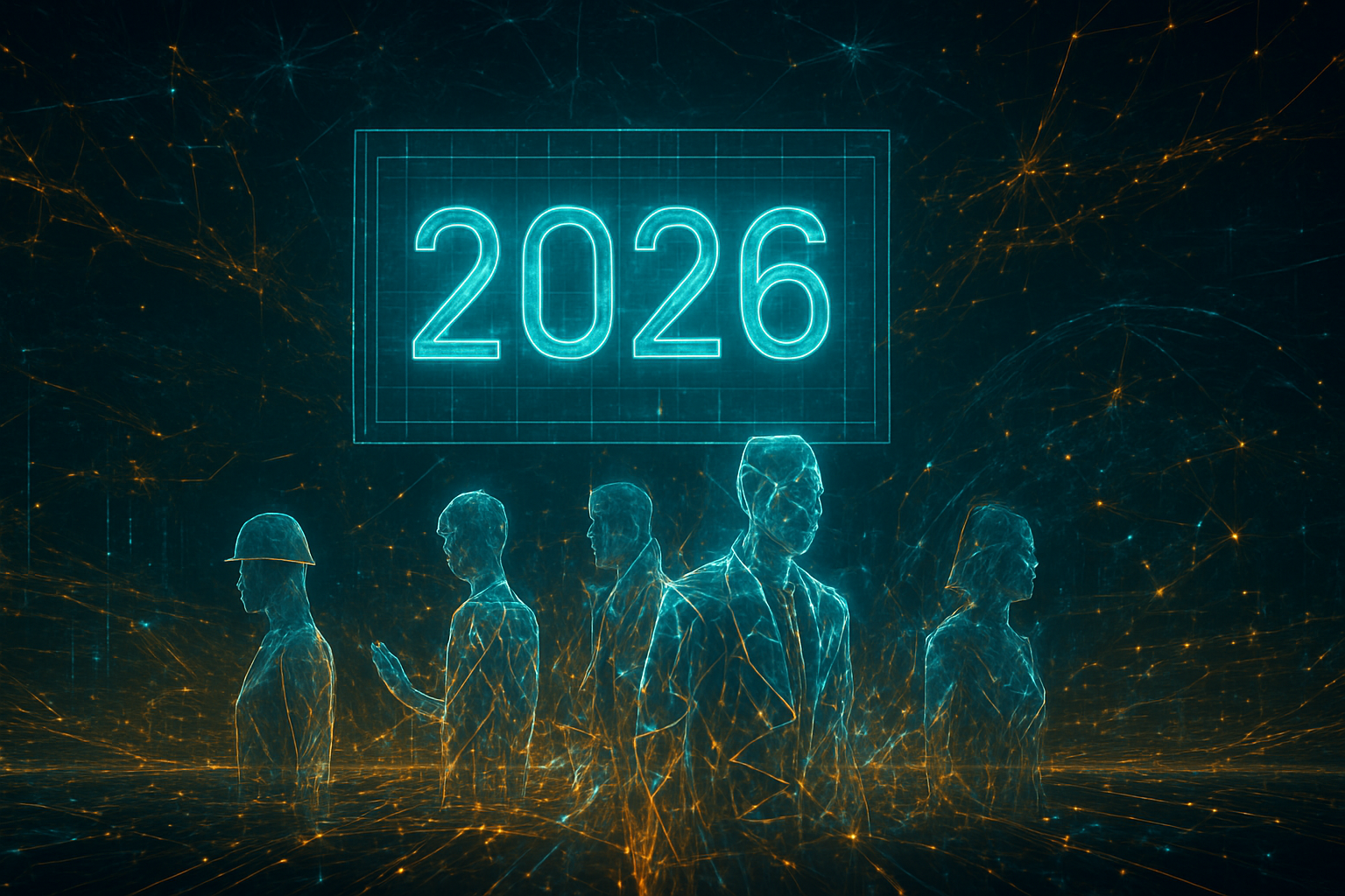
In a move that signals the definitive end of the traditional "syntax-first" era of software engineering, Collins Dictionary has officially named "Vibe Coding" its Word of the Year for 2025. This selection marks a profound cultural and technological pivot, moving the spotlight from 2024’s pop-culture "Brat" to a term that defines the intersection of human intent and machine execution. The choice reflects a year where the barrier between having an idea and shipping a functional application has effectively collapsed, replaced by a natural language-driven workflow that prioritizes the "vibe"—the high-level vision and user experience—over the manual orchestration of logic and code.
The announcement, made on November 6, 2025, highlights the explosive rise of a development philosophy where the "hottest new programming language is English." Collins lexicographers noted a massive surge in the term's usage following its popularization by AI luminary Andrej Karpathy in early 2025. As generative AI models have evolved from simple autocompletes to autonomous agents capable of managing entire repositories, "vibe coding" has transitioned from a Silicon Valley meme into a mainstream phenomenon, fundamentally altering how software is conceived, built, and maintained across the global economy.
The Technical Engine of the Vibe: From Autocomplete to Agentic Autonomy
Technically, vibe coding represents the transition from "copilots" to "agents." In late 2024 and throughout 2025, the industry saw the release of tools like Cursor 2.0 by Anysphere, which introduced "Composer"—a multi-file editing mode that coordinates changes across an entire codebase simultaneously. Unlike previous iterations of AI coding assistants that provided line-by-line suggestions, these agentic IDEs utilize massive context windows—such as Meta Platforms, Inc. (NASDAQ: META)'s Llama 4 Scout with its 10-million-token capacity—to "hold" an entire project in active memory. This allows the AI to maintain architectural consistency and understand complex inter-dependencies that were previously the sole domain of senior human engineers.
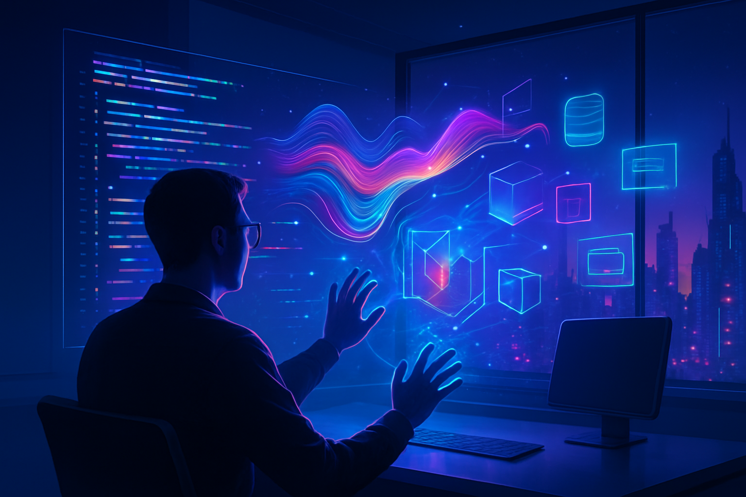
The technical specifications of 2025’s leading models, including Anthropic’s Claude 4.5 and OpenAI’s GPT-5/o1, have shifted the focus toward "System 2" reasoning. These models no longer just predict the next token; they engage in iterative self-correction and step-by-step verification. This capability is what enables a developer to "vibe" a feature into existence: the user provides a high-level prompt (e.g., "Add a real-time analytics dashboard with a retro-neon aesthetic"), and the agent plans the database schema, writes the frontend components, configures the API endpoints, and runs its own unit tests to verify the result.
Initial reactions from the research community have been polarized. While pioneers like Karpathy champion the efficiency of "giving in to the vibes" and embracing exponential productivity, others warn of a "vibe coding hangover." The primary technical concern is the potential for "spaghetti code"—AI-generated logic that functions correctly but lacks a clean, human-readable architecture. This has led to the emergence of "Context Engineering," a new discipline where developers focus on crafting the rules and constraints (the "context") that guide the AI, rather than writing the raw code itself.
The Corporate Arms Race: Hyperscalers vs. The New Guard
The rise of vibe coding has sparked a fierce competitive battle among tech giants and nimble startups. Anysphere, the creator of the Cursor editor, saw its valuation skyrocket to $9.9 billion in 2025, positioning itself as a legitimate threat to established workflows. In response, Microsoft (NASDAQ: MSFT) transformed GitHub Copilot into a "fully agentic partner" with the release of Agent Mode. By adopting the Model Context Protocol (MCP), Microsoft has allowed Copilot to act as a universal interface, connecting to external data sources like Jira and Slack to automate end-to-end project management.
Alphabet Inc. (NASDAQ: GOOGL) and Amazon.com, Inc. (NASDAQ: AMZN) have also launched major counter-offensives. Google’s "Antigravity IDE," powered by Gemini 3, features "Magic Testing," where AI agents autonomously open browsers to click through and validate UI changes, providing video reports of the results. Meanwhile, Amazon released "AWS Kiro," an agentic IDE specifically designed for "Spec-Driven Development." Kiro targets enterprise environments by requiring formal specifications before the AI begins "vibing," ensuring that the resulting code meets rigorous production-grade standards and security protocols.
This shift has significant implications for the startup ecosystem. Replit, with its "Replit Agent," has democratized app creation to the point where non-technical founders are building and scaling full-stack applications in days. This "Prompt-to-App" pipeline is disrupting the traditional outsourced development market, as small teams can now achieve the output previously reserved for large engineering departments. For major AI labs like OpenAI and Anthropic, the trend reinforces their position as the "operating systems" of the new economy, as their models serve as the underlying intelligence for every vibe-coding tool on the market.
The Cultural Shift: Democratization vs. The 'Clanker' Anxiety
Beyond the technical and corporate spheres, "Vibe Coding" reflects a broader societal tension in the AI era. The 2025 Collins Word of the Year shortlist included the term "clanker"—a derogatory slang for AI or robots—highlighting a growing friction between those who embrace AI-driven productivity and those who fear its impact on human agency and employment. Vibe coding sits at the center of this debate; it represents the ultimate democratization of technology, allowing anyone with an idea to become a "creator," yet it also threatens the traditional career path of the junior developer.
Comparisons have been drawn to previous milestones like the introduction of the spreadsheet or the transition from assembly language to C++. However, the speed of the vibe-coding revolution is unprecedented. Analysts have warned of a "$1.5 trillion technical debt" looming by 2027, as unvetted AI-generated code fills global repositories. The concern is that while the "vibe" of an application might be perfect today, the underlying "spaghetti" could create a complexity ceiling that makes future updates or security patches nearly impossible for humans to manage.
Despite these concerns, the impact on global innovation is undeniable. The "vibe" era has shifted the value proposition of a software engineer from "coder" to "architect and curator." In this new landscape, the most successful developers are those who can effectively communicate intent and maintain a high-level vision, rather than those who can memorize the intricacies of a specific syntax. This mirrors the broader AI trend of moving toward high-level human-machine collaboration across all creative fields.
The Horizon: Spec-Driven Development and Agentic Fleets
Looking forward, the evolution of vibe coding is expected to move toward "Autonomous Software Engineering." We are already seeing the emergence of "Agentic Fleets"—coordinated groups of specialized AI agents that handle different parts of the development lifecycle. One agent might focus exclusively on security audits, another on UI/UX, and a third on backend optimization, all orchestrated by a human "Vibe Manager." This multi-agent approach aims to solve the technical debt problem by building in automated checks and balances at every stage of the process.
The near-term focus for the industry will likely be "Spec-Driven Vibe Coding." To mitigate the risks of unvetted code, new tools will require developers to provide structured "vibes"—a combination of natural language, design mockups, and performance constraints—that the AI must adhere to. This will bring a level of rigor to the process that is currently missing from "pure" vibe coding. Experts predict that by 2026, the majority of enterprise software will be "vibe-first," with humans acting as the final reviewers and ethical gatekeepers of the AI's output.
A New Chapter in Human Creativity
The naming of "Vibe Coding" as the 2025 Word of the Year is more than just a linguistic curiosity; it is a recognition of a fundamental shift in how humanity interacts with machines. It marks the moment when software development transitioned from a specialized craft into a universal form of expression. While the "vibe coding hangover" and technical debt remain significant challenges that the industry must address, the democratization of creation that this movement represents is a landmark achievement in the history of artificial intelligence.
In the coming weeks and months, the tech world will be watching closely to see how the "Big Three" hyperscalers integrate these agentic capabilities into their core platforms. As the tension between "vibes" and "rigor" continues to play out, one thing is certain: the era of the manual coder is fading, replaced by a new generation of creators who can speak their visions into reality. The "vibe" is here to stay, and it is rewriting the world, one prompt at a time.
This content is intended for informational purposes only and represents analysis of current AI developments.
TokenRing AI delivers enterprise-grade solutions for multi-agent AI workflow orchestration, AI-powered development tools, and seamless remote collaboration platforms.
For more information, visit https://www.tokenring.ai/.