Tag: AI

  • Nvidia’s $5 Billion Intel Investment: Securing the Future of American AI and x86 Co-Design

    Nvidia’s $5 Billion Intel Investment: Securing the Future of American AI and x86 Co-Design

    In a move that has sent shockwaves through the global semiconductor industry, Nvidia (NASDAQ: NVDA) has officially finalized a $5 billion strategic investment in Intel (NASDAQ: INTC). The deal, completed today, December 29, 2025, grants Nvidia an approximate 5% ownership stake in its long-time rival, signaling an unprecedented era of cooperation between the two titans of American computing. This capital infusion arrives at a critical juncture for Intel, which has spent the last year navigating a complex restructuring under the leadership of CEO Lip-Bu Tan and a recent 10% equity intervention by the U.S. government.

    The partnership is far more than a financial lifeline; it represents a fundamental shift in the "chip wars." By securing a seat at Intel’s table, Nvidia has gained guaranteed access to domestic foundry capacity and, more importantly, a co-design agreement for the x86 architecture. This alliance aims to combine Nvidia’s dominant AI and graphics prowess with Intel’s legacy in CPU design and advanced manufacturing, creating a formidable domestic front against international competition and consolidating the U.S. semiconductor supply chain.

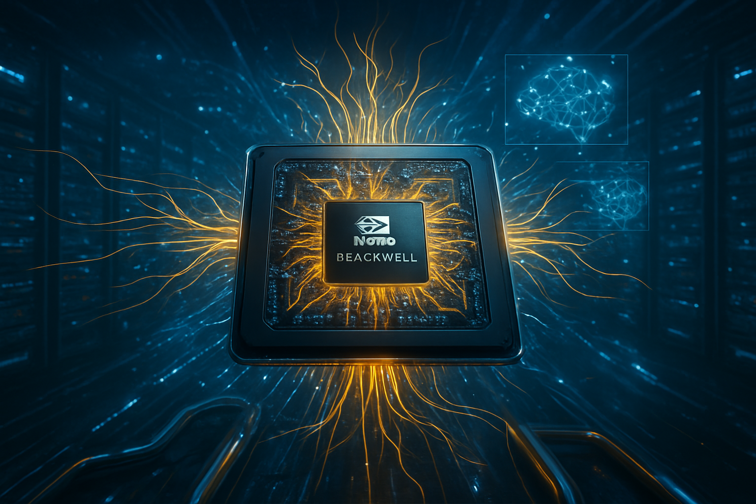
    The Technical Fusion: x86 Meets RTX

    At the heart of this deal is a groundbreaking co-design initiative: the "Intel x86 RTX SOC" (System-on-a-Chip). These new processors are designed to integrate Intel’s high-performance x86 CPU cores directly with Nvidia’s flagship RTX graphics chiplets within a single package. Unlike previous integrated graphics solutions, these "super-chips" leverage Nvidia’s NVLink interconnect technology, allowing for CPU-to-GPU bandwidth that dwarfs traditional PCIe connections. This integration is expected to redefine the high-end laptop and small-form-factor PC markets, providing a level of performance-per-watt that was previously unattainable in a unified architecture.

    The technical synergy extends into the data center. Intel is now tasked with manufacturing "Nvidia-custom" x86 CPUs. These chips will be marketed under the Nvidia brand to hyperscalers and enterprise clients, offering a high-performance x86 alternative to Nvidia’s existing ARM-based "Grace" CPUs. This dual-architecture strategy allows Nvidia to capture the vast majority of the server market that remains tethered to x86 software ecosystems while still pushing the boundaries of AI acceleration.

    Manufacturing these complex designs will rely heavily on Intel Foundry’s advanced packaging capabilities. The agreement highlights the use of Foveros 3D and EMIB (Embedded Multi-die Interconnect Bridge) technologies to stack and connect disparate silicon dies. While Nvidia is reportedly continuing its relationship with TSMC for its primary 3nm and 2nm AI GPU production due to yield considerations, the Intel partnership secures a massive domestic "Plan B" and a specialized line for these new hybrid products.

    Industry experts have reacted with a mix of awe and caution. "We are seeing the birth of a 'United States of Silicon,'" noted one senior research analyst. "By fusing the x86 instruction set with the world's leading AI hardware, Nvidia is essentially building a moat that neither ARM nor AMD can easily cross." However, some in the research community worry that such consolidation could stifle the very competition that drove the recent decade of rapid AI innovation.

    Competitive Fallout and Market Realignment

    The implications for the broader tech industry are profound. Advanced Micro Devices (NASDAQ: AMD), which has long been the only player offering both high-end x86 CPUs and competitive GPUs, now faces a combined front from its two largest rivals. The Intel-Nvidia alliance directly targets AMD’s stronghold in the APU (Accelerated Processing Unit) market, potentially squeezing AMD’s margins in both the gaming and data center sectors.

    For the "Magnificent Seven" and other hyperscalers—such as Microsoft (NASDAQ: MSFT), Alphabet (NASDAQ: GOOGL), and Amazon (NASDAQ: AMZN)—this deal simplifies the procurement of high-performance AI infrastructure. By offering a unified x86-RTX stack, Nvidia can provide a "turnkey" solution for AI-ready workstations and servers that are fully compatible with existing enterprise software. This could lead to a faster rollout of on-premise AI applications, as companies will no longer need to choose between x86 compatibility and peak AI performance.

    The ARM ecosystem also faces a strategic challenge. While Nvidia remains a major licensee of ARM technology, this $5 billion pivot toward Intel suggests that Nvidia views x86 as a vital component of its long-term strategy, particularly in the domestic market. This could slow the momentum of ARM-based Windows laptops and servers, as the "Intel x86 RTX" chips promise to deliver the performance users expect without the compatibility hurdles associated with ARM translation layers.

    A New Era for Semiconductor Sovereignty

    The wider significance of this deal cannot be overstated. It marks a pivotal moment in the quest for U.S. semiconductor sovereignty. Following the U.S. government’s 10% stake in Intel earlier in August 2025, Nvidia’s investment provides the private-sector validation needed to stabilize Intel’s foundry business. This "public-private-partnership" model ensures that the most advanced AI chips can be designed, manufactured, and packaged entirely within the United States, mitigating risks associated with geopolitical tensions in the Taiwan Strait.

    Historically, this milestone is comparable to the 1980s "Sematech" initiative, but on a much larger, corporate-driven scale. It reflects a shift from a globalized, "fabless" model back toward a more vertically integrated and geographically concentrated strategy. This consolidation of power, however, raises significant antitrust concerns. Regulators in the EU and China are already signaling they will closely scrutinize the co-design agreements to ensure that the x86 architecture remains accessible to other players and that Nvidia does not gain an unfair advantage in the AI software stack.

    Furthermore, the deal highlights the shifting definition of a "chip company." Nvidia is no longer just a GPU designer; it is now a stakeholder in the very fabric of the PC and server industry. This move mirrors the industry's broader trend toward "systems-on-silicon," where the value lies not in individual components, but in the tight integration of software, interconnects, and diverse processing units.

    The Road Ahead: 2026 and Beyond

    In the near term, the industry is bracing for the first wave of "Blue-Green" silicon (referring to Intel’s blue and Nvidia’s green branding). Prototypes of the x86 RTX SOCs are expected to be showcased at CES 2026, with mass production slated for the second half of the year. The primary challenge will be the software integration—ensuring that Nvidia’s CUDA platform and Intel’s OneAPI can work seamlessly across these hybrid chips.

    Longer term, the partnership could evolve into a full-scale manufacturing agreement where Nvidia moves more of its mainstream GPU production to Intel Foundry Services. Experts predict that if Intel’s 18A and 14A nodes reach maturity and high yields by 2027, Nvidia may shift a significant portion of its Blackwell-successor volume to domestic soil. This would represent a total transformation of the global supply chain, potentially ending the era of TSMC's absolute dominance in high-end AI silicon.

    However, the path is not without obstacles. Integrating two very different corporate cultures and engineering philosophies—Intel’s traditional "IDM" (Integrated Device Manufacturer) approach and Nvidia’s agile, software-first mindset—will be a monumental task. The success of the "Intel x86 RTX" line will depend on whether the performance gains of NVLink-on-x86 are enough to justify the premium pricing these chips will likely command.

    Final Reflections on a Seismic Shift

    Nvidia’s $5 billion investment in Intel is the most significant corporate realignment in the history of the semiconductor industry. It effectively ends the decades-long rivalry between the two companies in favor of a strategic partnership aimed at securing the future of American AI leadership. By combining Intel's manufacturing scale and x86 legacy with Nvidia's AI dominance, the two companies have created a "Silicon Superpower" that will be difficult for any competitor to match.

    As we move into 2026, the key metrics for success will be the yield rates of Intel's domestic foundries and the market adoption of the first co-designed chips. This development marks the end of the "fabless vs. foundry" era and the beginning of a "co-designed, domestic-first" era. For the tech industry, the message is clear: the future of AI is being built on a foundation of integrated, domestic silicon, and the old boundaries between CPU and GPU companies have officially dissolved.


    This content is intended for informational purposes only and represents analysis of current AI developments.

    TokenRing AI delivers enterprise-grade solutions for multi-agent AI workflow orchestration, AI-powered development tools, and seamless remote collaboration platforms.
    For more information, visit https://www.tokenring.ai/.

  • The Silicon Giant: Cerebras WSE-3 Shatters LLM Speed Records as Q2 2026 IPO Approaches

    The Silicon Giant: Cerebras WSE-3 Shatters LLM Speed Records as Q2 2026 IPO Approaches

    As the artificial intelligence industry grapples with the "memory wall" that has long constrained the performance of traditional graphics processing units (GPUs), Cerebras Systems has emerged as a formidable challenger to the status quo. On December 29, 2025, the company’s Wafer-Scale Engine 3 (WSE-3) and the accompanying CS-3 system have officially redefined the benchmarks for Large Language Model (LLM) inference, delivering speeds that were once considered theoretically impossible. By utilizing an entire 300mm silicon wafer as a single processor, Cerebras has bypassed the traditional bottlenecks of high-bandwidth memory (HBM), setting the stage for a highly anticipated initial public offering (IPO) targeted for the second quarter of 2026.

    The significance of the CS-3 system lies not just in its raw power, but in its ability to provide instantaneous, real-time responses for the world’s most complex AI models. While industry leaders have focused on throughput for thousands of simultaneous users, Cerebras has prioritized the "per-user" experience, achieving inference speeds that enable AI agents to "think" and "reason" at a pace that mimics human cognitive speed. This development comes at a critical juncture for the company as it clears the final regulatory hurdles and prepares to transition from a venture-backed disruptor to a public powerhouse on the Nasdaq (CBRS).

    Technical Dominance: Breaking the Memory Wall

    The Cerebras WSE-3 is a marvel of semiconductor engineering, boasting a staggering 4 trillion transistors and 900,000 AI-optimized cores manufactured on a 5nm process by Taiwan Semiconductor Manufacturing Company (NYSE: TSM). Unlike traditional chips from NVIDIA (NASDAQ: NVDA) or Advanced Micro Devices (NASDAQ: AMD), which must shuttle data back and forth between the processor and external memory, the WSE-3 keeps the entire model—or significant portions of it—within 44GB of on-chip SRAM. This architecture provides a memory bandwidth of 21 petabytes per second (PB/s), which is approximately 2,600 times faster than NVIDIA’s flagship Blackwell B200.

    In practical terms, this massive bandwidth translates into unprecedented LLM inference speeds. Recent benchmarks for the CS-3 system show the Llama 3.1 70B model running at a blistering 2,100 tokens per second per user—roughly eight times faster than NVIDIA’s H200 and double the speed of the Blackwell architecture for single-user latency. Even the massive Llama 3.1 405B model, which typically requires multiple networked GPUs to function, runs at 970 tokens per second on the CS-3. These speeds are not merely incremental improvements; they represent what Cerebras CEO Andrew Feldman calls the "broadband moment" for AI, where the latency of interaction finally drops below the threshold of human perception.

    The AI research community has reacted with a mixture of awe and strategic recalibration. Experts from organizations like Artificial Analysis have noted that Cerebras is effectively solving the "latency problem" for agentic workflows, where a model must perform dozens of internal reasoning steps before providing an answer. By reducing the time per step from seconds to milliseconds, the CS-3 enables a new class of "thinking" AI that can navigate complex software environments and perform multi-step tasks in real-time without the lag that characterizes current GPU-based clouds.

    Market Disruption and the Path to IPO

    Cerebras' technical achievements are being mirrored by its aggressive financial maneuvers. After a period of regulatory uncertainty in 2024 and 2025 regarding its relationship with the Abu Dhabi-based AI firm G42, Cerebras has successfully cleared its path to the public markets. Reports indicate that G42 has fully divested its ownership stake to satisfy U.S. national security reviews, and Cerebras is now moving forward with a Q2 2026 IPO target. Following a massive $1.1 billion Series G funding round in late 2025 led by Fidelity and Atreides Management, the company's valuation has surged toward the tens of billions, with analysts predicting a listing valuation exceeding $15 billion.

    The competitive implications for the tech industry are profound. While NVIDIA remains the undisputed king of training and high-throughput data centers, Cerebras is carving out a high-value niche in the inference market. Startups and enterprise giants alike—such as Meta (NASDAQ: META) and Microsoft (NASDAQ: MSFT)—stand to benefit from a diversified hardware ecosystem. Cerebras has already priced its inference API at a competitive $0.60 per 1 million tokens for Llama 3.1 70B, a move that directly challenges the margins of established cloud providers like Amazon (NASDAQ: AMZN) Web Services and Google (NASDAQ: GOOGL).

    This disruption extends beyond pricing. By offering a "weight streaming" architecture that treats an entire cluster as a single logical processor, Cerebras simplifies the software stack for developers who are tired of the complexities of managing multi-GPU clusters and NVLink interconnects. For AI labs focused on low-latency applications—such as real-time translation, high-frequency trading, and autonomous robotics—the CS-3 offers a strategic advantage that traditional GPU clusters struggle to match.

    The Global AI Landscape and Agentic Trends

    The rise of wafer-scale computing fits into a broader shift in the AI landscape toward "Agentic AI"—systems that don't just generate text but actively solve problems. As models like Llama 4 (Maverick) and DeepSeek-R1 become more sophisticated, they require hardware that can support high-speed internal "Chain of Thought" processing. The WSE-3 is perfectly positioned for this trend, as its architecture excels at the sequential processing required for reasoning agents.

    However, the shift to wafer-scale technology is not without its challenges and concerns. The CS-3 system is a high-power beast, drawing 23 kilowatts of electricity per unit. While Cerebras argues that a single CS-3 replaces dozens of traditional GPUs—thereby reducing the total power footprint for a given workload—the physical infrastructure required to support such high-density computing is a barrier to entry for smaller data centers. Furthermore, the reliance on a single, massive piece of silicon introduces manufacturing yield risks that smaller, chiplet-based designs like those from NVIDIA and AMD are better equipped to handle.

    Comparisons to previous milestones, such as the transition from CPUs to GPUs for deep learning in the early 2010s, are becoming increasingly common. Just as the GPU unlocked the potential of neural networks, wafer-scale engines are unlocking the potential of real-time, high-reasoning agents. The move toward specialized inference hardware suggests that the "one-size-fits-all" era of the GPU may be evolving into a more fragmented and specialized hardware market.

    Future Horizons: Llama 4 and Beyond

    Looking ahead, the roadmap for Cerebras involves even deeper integration with the next generation of open-source and proprietary models. Early benchmarks for Llama 4 (Maverick) on the CS-3 have already reached 2,522 tokens per second, suggesting that as models become more efficient, the hardware's overhead remains minimal. The near-term focus for the company will be diversifying its customer base beyond G42, targeting U.S. government agencies (DoE, DoD) and large-scale enterprise cloud providers who are eager to reduce their dependence on the NVIDIA supply chain.

    In the long term, the challenge for Cerebras will be maintaining its lead as competitors like Groq and SambaNova also target the low-latency inference market with their own specialized architectures. The "inference wars" of 2026 are expected to be fought on the battlegrounds of energy efficiency and software ease-of-use. Experts predict that if Cerebras can successfully execute its IPO and use the resulting capital to scale its manufacturing and software support, it could become the primary alternative to NVIDIA for the next decade of AI development.

    A New Era for AI Infrastructure

    The Cerebras WSE-3 and the CS-3 system represent more than just a faster chip; they represent a fundamental rethink of how computers should be built for the age of intelligence. By shattering the 1,000-token-per-second barrier for massive models, Cerebras has proved that the "memory wall" is not an insurmountable law of physics, but a limitation of traditional design. As the company prepares for its Q2 2026 IPO, it stands as a testament to the rapid pace of innovation in the semiconductor industry.

    The key takeaways for investors and tech leaders are clear: the AI hardware market is no longer a one-horse race. While NVIDIA's ecosystem remains dominant, the demand for specialized, ultra-low-latency inference is creating a massive opening for wafer-scale technology. In the coming months, all eyes will be on the SEC filings and the performance of the first Llama 4 deployments on CS-3 hardware. If the current trajectory holds, the "Silicon Giant" from Sunnyvale may very well be the defining story of the 2026 tech market.


    This content is intended for informational purposes only and represents analysis of current AI developments.

    TokenRing AI delivers enterprise-grade solutions for multi-agent AI workflow orchestration, AI-powered development tools, and seamless remote collaboration platforms.
    For more information, visit https://www.tokenring.ai/.

  • Silicon Sovereignty: Apple Qualifies Intel’s 18A Node in Seismic Shift for M-Series Manufacturing

    Silicon Sovereignty: Apple Qualifies Intel’s 18A Node in Seismic Shift for M-Series Manufacturing

    In a move that signals a tectonic shift in the global semiconductor landscape, reports have emerged as of late December 2025 that Apple Inc. (NASDAQ: AAPL) has successfully entered the critical qualification phase for Intel Corporation’s (NASDAQ: INTC) 18A manufacturing process. This development marks the first time since the "Apple Silicon" transition in 2020 that the iPhone maker has seriously considered a primary manufacturing partner other than Taiwan Semiconductor Manufacturing Company (NYSE: TSM). By qualifying the 1.8nm-class node for future entry-level M-series chips, Apple is effectively ending TSMC’s decade-long monopoly on its high-end processor production, a strategy aimed at diversifying its supply chain and securing domestic U.S. manufacturing capabilities.

    The immediate significance of this partnership cannot be overstated. For Intel, securing Apple as a foundry customer is the ultimate validation of its "five nodes in four years" (5N4Y) turnaround strategy led by CEO Pat Gelsinger. For the broader technology industry, it represents a pivotal moment in the "re-shoring" of advanced chipmaking to American soil. As geopolitical tensions continue to cast a shadow over the Taiwan Strait, Apple’s move to utilize Intel’s Arizona-based "Fab 52" provides a necessary hedge against regional instability while potentially lowering logistics costs and lead times for its highest-volume products, such as the MacBook Air and iPad Pro.

    Technical Breakthroughs: RibbonFET and the PowerVia Advantage

    At the heart of this historic partnership is Intel’s 18A node, a 1.8nm-class process that introduces two of the most significant architectural changes in transistor design in over a decade. The first is RibbonFET, Intel’s proprietary implementation of Gate-All-Around (GAA) technology. Unlike the FinFET transistors used in previous generations, RibbonFET surrounds the conducting channel with the gate on all four sides. This allows for superior electrostatic control, drastically reducing power leakage—a critical requirement for the thin-and-light designs of Apple’s portable devices—while simultaneously increasing switching speeds.

    The second, and perhaps more disruptive, technical milestone is PowerVia, the industry’s first commercial implementation of backside power delivery. By moving power routing to the back of the silicon wafer and keeping signal routing on the front, Intel has solved one of the most persistent bottlenecks in chip design: "IR drop" or voltage loss. According to technical briefings from late 2025, PowerVia allows for a 5% to 10% improvement in cell utilization and a significant boost in performance-per-watt. Reports indicate that Apple has specifically been working with the 18AP (Performance) variant, a specialized version of the node optimized for high-efficiency mobile workloads, which offers an additional 15% to 20% improvement in performance-per-watt over the standard 18A process.

    Initial reactions from the semiconductor research community have been cautiously optimistic. While early reports from partners like Broadcom (NASDAQ: AVGO) and NVIDIA (NASDAQ: NVDA) suggested that Intel’s 18A yields were initially hovering in the 60% to 65% range—below the 70% threshold typically required for high-margin mass production—the news that Apple has received the PDK 0.9.1 GA (Process Design Kit) suggests those hurdles are being cleared. Industry experts note that Apple’s rigorous qualification standards are the "gold seal" of foundry reliability; if Intel can meet Apple’s stringent requirements for the M-series, it proves the 18A node is ready for the most demanding consumer electronics in the world.

    A New Power Dynamic: Disrupting the Foundry Monopoly

    The strategic implications of this partnership extend far beyond technical specifications. By bringing Intel into the fold, Apple gains immense leverage over TSMC. For years, TSMC has been the sole provider of the world’s most advanced nodes, allowing it to command premium pricing and dictate production schedules. With Intel 18A now a viable alternative, Apple can exert downward pressure on TSMC’s 2nm (N2) pricing. This "dual-foundry" strategy will likely see TSMC retain the manufacturing rights for the high-end "Pro," "Max," and "Ultra" variants of the M-series, while Intel handles the high-volume base models, estimated to reach 15 to 20 million units annually.

    For Intel, this is a transformative win that repositions its Intel Foundry division as a top-tier competitor to TSMC and Samsung (KRX: 005930). Following the news of Apple’s qualification efforts in November 2025, Intel’s stock saw a double-digit surge, reflecting investor confidence that the company can finally monetize its massive capital investments in U.S. manufacturing. The partnership also creates a "halo effect" for Intel Foundry, making it a more attractive option for other tech giants like Microsoft (NASDAQ: MSFT) and Amazon (NASDAQ: AMZN), who are increasingly designing their own custom AI and server silicon.

    However, this development poses a significant challenge to TSMC’s market dominance. While TSMC’s N2 node is still widely considered the gold standard for power efficiency, the geographic concentration of its facilities has become a strategic liability. Apple’s shift toward Intel signals to the rest of the industry that "geopolitical de-risking" is no longer a theoretical preference but a practical manufacturing requirement. If more "fabless" companies follow Apple’s lead, the semiconductor industry could see a more balanced distribution of power between East and West for the first time in thirty years.

    The Broader AI Landscape and the "Made in USA" Mandate

    The Apple-Intel 18A partnership is a cornerstone of the broader trend toward vertical integration and localized supply chains. As AI-driven workloads become the primary focus of consumer hardware, the need for specialized silicon that balances high-performance neural engines with extreme power efficiency has never been greater. Intel’s 18A node is designed with these AI-centric architectures in mind, offering the density required to pack more transistors into the small footprints of next-generation iPads and MacBooks. This fits perfectly into Apple's "Apple Intelligence" roadmap, which demands increasingly powerful on-device processing to handle complex LLM (Large Language Model) tasks without sacrificing battery life.

    This move also aligns with the objectives of the U.S. CHIPS and Science Act. By qualifying a node that will be manufactured in Arizona, Apple is effectively participating in a national effort to secure the semiconductor supply chain. This reduces the risk of global disruptions caused by potential conflicts or pandemics. Comparisons are already being drawn to the 2010s, when Apple transitioned from Samsung to TSMC; that shift redefined the mobile industry, and many analysts believe this return to a domestic partner could have an even greater impact on the future of computing.

    There are, however, potential concerns regarding the transition. Moving a chip design from TSMC’s ecosystem to Intel’s requires significant engineering resources. Apple’s "qualification" of the node does not yet equal a signed high-volume contract for the entire product line. Some industry skeptics worry that if Intel’s yields do not reach the 70-80% mark by mid-2026, Apple may scale back its commitment, potentially leaving Intel with massive, underutilized capacity. Furthermore, the complexity of PowerVia and RibbonFET introduces new manufacturing risks that could lead to delays if not managed perfectly.

    Looking Ahead: The Road to 2027

    The near-term roadmap for this partnership is clear. Apple is expected to reach a final "go/no-go" decision by the first quarter of 2026, following the release of Intel’s finalized PDK 1.0. If the qualification continues on its current trajectory, the industry expects to see the first Intel-manufactured Apple M-series chips enter mass production in the second or third quarter of 2027. These chips will likely power a refreshed MacBook Air and perhaps a new generation of iPad Pro, marking the commercial debut of "Apple Silicon: Made in America."

    Long-term, this partnership could expand to include iPhone processors (the A-series) or even custom AI accelerators for Apple’s data centers. Experts predict that the success of the 18A node will determine the trajectory of the semiconductor industry for the next decade. If Intel delivers on its performance promises, it could trigger a massive migration of U.S. chip designers back to domestic foundries. The primary challenge remains the execution of High-NA EUV (Extreme Ultraviolet) lithography, a technology Intel is betting heavily on to maintain its lead over TSMC in the sub-2nm era.

    Summary of a Historic Realignment

    The qualification of Intel’s 18A node by Apple represents a landmark achievement in semiconductor engineering and a strategic masterstroke in corporate diplomacy. By bridging the gap between the world’s leading consumer electronics brand and the resurgent American chipmaker, this partnership addresses the two biggest challenges of the modern tech era: the need for unprecedented computational power for AI and the necessity of a resilient, diversified supply chain.

    As we move into 2026, the industry will be watching Intel’s yield rates and Apple’s final production orders with intense scrutiny. The significance of this development in AI history is profound; it provides the physical foundation upon which the next generation of on-device intelligence will be built. For now, the "historic" nature of this partnership is clear: Apple and Intel, once rivals and then distant acquaintances, have found a common cause in the pursuit of silicon sovereignty.


    This content is intended for informational purposes only and represents analysis of current AI and semiconductor developments as of December 29, 2025.

    TokenRing AI delivers enterprise-grade solutions for multi-agent AI workflow orchestration, AI-powered development tools, and seamless remote collaboration platforms. For more information, visit https://www.tokenring.ai/.

  • The Light Speed Revolution: Silicon Photonics Hits Commercial Prime as Marvell and Broadcom Reshape AI Infrastructure

    The Light Speed Revolution: Silicon Photonics Hits Commercial Prime as Marvell and Broadcom Reshape AI Infrastructure

    The artificial intelligence industry has reached a pivotal infrastructure milestone as silicon photonics transitions from a long-promised laboratory curiosity to the backbone of global data centers. In a move that signals the end of the "copper era" for high-performance computing, Marvell Technology (NASDAQ: MRVL) officially announced its definitive agreement to acquire Celestial AI on December 2, 2025, for an initial value of $3.25 billion. This acquisition, coupled with Broadcom’s (NASDAQ: AVGO) staggering record of $20 billion in AI hardware revenue for fiscal year 2025, confirms that light-based interconnects are no longer a luxury—they are a necessity for the next generation of generative AI.

    The commercial breakthrough comes at a critical time when traditional electrical signaling is hitting physical limits. As AI models like OpenAI’s "Titan" project demand unprecedented levels of data throughput, the industry is shifting toward optical solutions to solve the "memory wall"—the bottleneck where processors spend more time waiting for data than computing it. This convergence of Marvell’s strategic M&A and Broadcom’s dominant market performance marks the beginning of a new epoch in AI hardware, where silicon photonics provides the massive bandwidth and energy efficiency required to sustain the current pace of AI scaling.

    Breaking the Memory Wall: The Technical Leap to Photonic Fabrics

    The centerpiece of this technological shift is the "Photonic Fabric," a proprietary architecture developed by Celestial AI that Marvell is now integrating into its portfolio. Unlike traditional pluggable optics that sit at the edge of a motherboard, Celestial AI’s technology utilizes an Optical Multi-Chip Interconnect Bridge (OMIB). This allows for 3D packaging where optical interconnects are placed directly on the silicon substrate alongside AI accelerators (XPUs) and High Bandwidth Memory (HBM). By using light to transport data across these components, the Photonic Fabric delivers 25 times greater bandwidth while reducing latency and power consumption by a factor of ten compared to existing copper-based solutions.

    Broadcom (NASDAQ: AVGO) has simultaneously pushed the envelope with its own optical innovations, recently unveiling the Tomahawk 6 "Davidson" switch. This 102.4 Tbps Ethernet switch is the first to utilize 200G-per-lane Co-Packaged Optics (CPO). By integrating the optical engines directly into the switch package, Broadcom has slashed the energy required to move a bit of data, a feat previously thought impossible at these speeds. The industry's move to 1.6T and eventually 3.2T interconnects is now being realized through these advancements in silicon photonics, allowing hundreds of individual chips to function as a single, massive "virtual" processor.

    This shift represents a fundamental departure from the "scale-out" networking of the past decade. Previously, data centers connected clusters of servers using standard networking cables, which introduced significant lag. The new silicon photonics paradigm enables "scale-up" architectures, where the entire rack—or even multiple racks—is interconnected via a seamless web of light. This allows for near-instantaneous memory sharing across thousands of GPUs, effectively neutralizing the physical distance between chips and allowing larger models to be trained in a fraction of the time.

    Initial reactions from the AI research community have been overwhelmingly positive, with experts noting that these hardware breakthroughs are the "missing link" for trillion-parameter models. By moving the data bottleneck from the electrical domain to the optical domain, engineers can finally match the raw processing power of modern chips with a communication infrastructure that can keep up. The integration of 3nm Digital Signal Processors (DSPs) like Broadcom’s Sian3 further optimizes this ecosystem, ensuring that the transition to light is as power-efficient as possible.

    Market Dominance and the New Competitive Landscape

    The acquisition of Celestial AI positions Marvell Technology (NASDAQ: MRVL) as a formidable challenger to the established order of AI networking. By securing the Photonic Fabric technology, Marvell is targeting a $1 billion annualized revenue run rate for its optical business by 2029. This move is a direct shot across the bow of Nvidia (NASDAQ: NVDA) (NASDAQ: NVDA), which has traditionally dominated the AI interconnect space with its proprietary NVLink technology. Marvell’s strategy is to offer an open, high-performance alternative that appeals to hyperscalers like Google (NASDAQ: GOOGL) and Meta (NASDAQ: META), who are increasingly looking to decouple their hardware stacks from single-vendor ecosystems.

    Broadcom, meanwhile, has solidified its status as the "arms dealer" of the AI era. With AI revenue surging to $20 billion in 2025—a 65% year-over-year increase—Broadcom’s dominance in custom ASICs and high-end switching is unparalleled. Their record Q4 revenue of $6.5 billion was largely driven by the massive deployment of custom AI accelerators for major cloud providers. By leading the charge in Co-Packaged Optics, Broadcom is ensuring that it remains the primary partner for any firm building a massive AI cluster, effectively gatekeeping the physical layer of the AI revolution.

    The competitive implications for startups and smaller AI labs are profound. As the cost of building state-of-the-art optical infrastructure rises, the barrier to entry for training "frontier" models becomes even higher. However, the availability of standardized silicon photonics products from Marvell and Broadcom could eventually democratize access to high-performance interconnects, allowing smaller players to build more efficient clusters using off-the-shelf components rather than expensive, proprietary systems.

    For the tech giants, this development is a strategic win. Companies like Meta (NASDAQ: META) have already begun trialing Broadcom’s CPO solutions to lower the massive electricity bills associated with their AI data centers. As silicon photonics reduces the power overhead of data movement, these companies can allocate more of their power budget to actual computation, maximizing the return on their multi-billion dollar infrastructure investments. The market is now seeing a clear bifurcation: companies that master the integration of light and silicon will lead the next decade of AI, while those reliant on traditional copper interconnects risk being left in the dark.

    The Broader Significance: Sustaining the AI Boom

    The commercialization of silicon photonics is more than just a hardware upgrade; it is a vital survival mechanism for the AI industry. As the world grapples with the environmental impact of massive data centers, the energy efficiency gains provided by optical interconnects are essential. By reducing the power required for data transmission by 90%, silicon photonics offers a path toward sustainable AI scaling. This shift is critical as global power grids struggle to keep pace with the exponential demand for AI compute, turning energy efficiency into a competitive "moat" for the most advanced tech firms.

    This milestone also represents a significant extension of Moore’s Law. For years, skeptics argued that the end of traditional transistor scaling would lead to a plateau in computing performance. Silicon photonics bypasses this limitation by focusing on the "interconnect bottleneck" rather than just the raw transistor count. By improving the speed at which data moves between chips, the industry can continue to see massive performance gains even as individual processors face diminishing returns from further miniaturization.

    Comparisons are already being drawn to the transition from dial-up internet to fiber optics. Just as fiber optics revolutionized global communications by enabling the modern internet, silicon photonics is poised to do the same for internal computer architectures. This is the first time in the history of computing that optical technology has been integrated so deeply into the chip packaging itself, marking a permanent shift in how we design and build high-performance systems.

    However, the transition is not without concerns. The complexity of manufacturing silicon photonics at scale remains a significant challenge. The precision required to align laser sources with silicon waveguides is measured in nanometers, and any manufacturing defect can render an entire multi-thousand-dollar chip useless. Furthermore, the industry must now navigate a period of intense standardization, as different vendors vie to make their optical protocols the industry standard. The outcome of these "standards wars" will dictate the shape of the AI industry for the next twenty years.

    Future Horizons: From Data Centers to the Edge

    Looking ahead, the near-term focus will be the rollout of 1.6T and 3.2T optical networks throughout 2026 and 2027. Experts predict that the success of the Marvell-Celestial AI integration will trigger a wave of further consolidation in the semiconductor industry, as other players scramble to acquire optical IP. We are likely to see "optical-first" AI architectures where the processor and memory are no longer distinct units but are instead part of a unified, light-driven compute fabric.

    In the long term, the applications of silicon photonics could extend beyond the data center. While currently too expensive for consumer electronics, the maturation of the technology could eventually bring optical interconnects to high-end workstations and even specialized edge AI devices. This would enable "AI at the edge" with capabilities that currently require a cloud connection, such as real-time high-fidelity language translation or complex autonomous navigation, all while maintaining strict power efficiency.

    The next major challenge for the industry will be the integration of "on-chip" lasers. Currently, most silicon photonics systems rely on external laser sources, which adds complexity and potential points of failure. Research into integrating light-emitting materials directly into the silicon manufacturing process is ongoing, and a breakthrough in this area would represent the final piece of the silicon photonics puzzle. If successful, this would allow for truly monolithic optical chips, further driving down costs and increasing performance.

    A New Era of Luminous Computing

    The events of late 2025—Marvell’s multi-billion dollar bet on Celestial AI and Broadcom’s record-shattering AI revenue—will be remembered as the moment silicon photonics reached its commercial tipping point. The transition from copper to light is no longer a theoretical goal but a market reality that is reshaping the balance of power in the semiconductor industry. By solving the memory wall and drastically reducing power consumption, silicon photonics has provided the necessary foundation for the next decade of AI advancement.

    The key takeaway for the industry is that the "infrastructure bottleneck" is finally being broken. As light-based interconnects become standard, the focus will shift from how to move data to how to use it most effectively. This development is a testament to the ingenuity of the semiconductor community, which has successfully married the worlds of photonics and electronics to overcome the physical limits of traditional computing.

    In the coming weeks and months, investors and analysts will be closely watching the regulatory approval process for the Marvell-Celestial AI deal and Broadcom’s initial shipments of the Tomahawk 6 "Davidson" switch. These milestones will serve as the first real-world tests of the silicon photonics era. As the first light-driven AI clusters come online, the true potential of this technology will finally be revealed, ushering in a new age of luminous, high-efficiency computing.


    This content is intended for informational purposes only and represents analysis of current AI developments.

    TokenRing AI delivers enterprise-grade solutions for multi-agent AI workflow orchestration, AI-powered development tools, and seamless remote collaboration platforms.
    For more information, visit https://www.tokenring.ai/.

  • The Glass Frontier: Intel and Rapidus Lead the Charge into the Next Era of AI Hardware

    The Glass Frontier: Intel and Rapidus Lead the Charge into the Next Era of AI Hardware

    The transition to glass substrates is driven by the failure of organic materials (like ABF and BT resins) to cope with the extreme heat and structural demands of massive AI "superchips." Glass offers a Coefficient of Thermal Expansion (CTE) that closely matches that of silicon (3–7 ppm/°C), which drastically reduces the risk of warpage during the high-temperature manufacturing processes required for advanced 2nm and 1.4nm nodes. Furthermore, glass is an exceptional electrical insulator with significantly lower dielectric loss (Df) and a lower dielectric constant (Dk) than silicon-based interposers. This allows for signal speeds to double while cutting insertion loss in half—a critical requirement for the high-frequency data transfers essential for 5G, 6G, and ultra-fast AI training.

    Technically, the "magic" of glass lies in Through-Glass Vias (TGVs). These microscopic vertical interconnects allow for a 10-fold increase in interconnect density compared to traditional organic substrates. This density enables thousands of Input/Output (I/O) bumps, allowing multiple chiplets—CPUs, GPUs, and High Bandwidth Memory (HBM)—to be packed closer together with minimal latency. At SEMICON Japan in December 2025, Rapidus demonstrated the sheer scale of this potential by unveiling a 600mm x 600mm glass panel-level packaging (PLP) prototype. Unlike traditional 300mm round silicon wafers, these massive square panels can yield up to 10 times more interposers, significantly reducing material waste and enabling the creation of "monster" packages that can house up to 24 HBM4 dies alongside a multi-tile GPU.

    Market Dynamics: A High-Stakes Race for Dominance

    Intel is currently the undisputed leader in the "Glass War," having invested over a decade of R&D into the technology. The company's Arizona-based pilot line is already operational, and Intel is on track to integrate glass substrates into its high-volume manufacturing (HVM) roadmap by late 2026. This head start provides Intel with a significant strategic advantage, potentially allowing them to reclaim the lead in the foundry business by offering packaging capabilities that Taiwan Semiconductor Manufacturing Co. (NYSE: TSM) is not expected to match at scale until 2028 or 2029 with its "CoPoS" (Chip-on-Panel-on-Substrate) initiative.

    However, the competition is intensifying rapidly. Samsung Electronics (KRX: 005930) has fast-tracked its glass substrate development, leveraging its existing expertise in large-scale glass manufacturing from its display division. Samsung is currently building a pilot line at its Sejong facility and aims for a 2026-2027 rollout, potentially positioning itself as a primary alternative for AI giants like NVIDIA and Advanced Micro Devices (NASDAQ: AMD) who are desperate to diversify their supply chains away from a single source. Meanwhile, the emergence of Rapidus as a serious contender with its panel-level prototype suggests that the Japanese semiconductor ecosystem is successfully leveraging its legacy in LCD technology to leapfrog current packaging constraints.

    Redefining the AI Landscape and Moore’s Law

    The wider significance of glass substrates lies in their role as the "enabling platform" for the post-Moore's Law era. As it becomes increasingly difficult to shrink transistors further, the industry has turned to heterogeneous integration—stacking and stitching different chips together. Glass substrates provide the structural integrity needed to build these massive 3D structures. Intel’s stated goal of reaching 1 trillion transistors on a single package by 2030 is virtually impossible without the flatness and thermal stability provided by glass.

    This development also addresses the critical "power wall" in AI data centers. The extreme flatness of glass allows for more reliable implementation of Backside Power Delivery (such as Intel’s PowerVia technology) at the package level. This reduces power noise and improves overall energy efficiency by an estimated 15% to 20%. In an era where AI power consumption is a primary concern for hyperscalers and environmental regulators alike, the efficiency gains from glass substrates could be just as important as the performance gains.

    The Road to 2026 and Beyond

    Looking ahead, the next 12 to 18 months will be focused on solving the remaining engineering hurdles of glass: namely, fragility and handling. While glass is structurally superior once assembled, it is notoriously difficult to handle in a high-speed factory environment without cracking. Companies like Rapidus are working closely with equipment manufacturers to develop specialized "glass-safe" robotic handling systems and laser-drilling techniques for TGVs. If these challenges are met, the shift to 600mm square panels could drop the cost of manufacturing massive AI interposers by as much as 40% by 2027.

    In the near term, expect to see the first commercial glass-packaged chips appearing in high-end server environments. These will likely be specialized AI accelerators or high-end Xeon processors designed for the most demanding scientific computing tasks. As the ecosystem matures, we can anticipate the technology trickling down to consumer-grade high-end gaming GPUs and workstations, where thermal management is a constant struggle. The ultimate goal is a fully standardized glass-based ecosystem that allows for "plug-and-play" chiplet integration from various vendors.

    Conclusion: A New Foundation for Computing

    The move to glass substrates marks the beginning of a new chapter in semiconductor history. It is a transition that validates the industry's shift from "system-on-chip" to "system-in-package." By solving the thermal and density bottlenecks that have plagued organic substrates, Intel and Rapidus are paving the way for a new generation of AI hardware that was previously thought to be physically impossible.

    As we move into 2026, the industry will be watching closely to see if Intel can successfully execute its high-volume rollout and if Rapidus can translate its impressive prototype into a viable manufacturing reality. The stakes are immense; the winner of the glass substrate race will likely hold the keys to the world's most powerful AI systems for the next decade. For now, the "Glass War" is just beginning, and it promises to be the most consequential battle in the tech industry's ongoing evolution.


    This content is intended for informational purposes only and represents analysis of current AI developments.

    TokenRing AI delivers enterprise-grade solutions for multi-agent AI workflow orchestration, AI-powered development tools, and seamless remote collaboration platforms.
    For more information, visit https://www.tokenring.ai/.

  • HBM4 Wars: Samsung and SK Hynix Fast-Track the Future of AI Memory

    HBM4 Wars: Samsung and SK Hynix Fast-Track the Future of AI Memory

    The high-stakes race for semiconductor supremacy has entered a blistering new phase as the industry’s titans prepare for the "HBM4 Wars." With artificial intelligence workloads demanding unprecedented memory bandwidth, Samsung Electronics (KRX: 005930) and SK Hynix (KRX: 000660) have both officially fast-tracked their next-generation High Bandwidth Memory (HBM4) for mass production in early 2026. This acceleration, moving the timeline up by nearly six months from original projections, signals a desperate scramble to supply the hardware backbone for NVIDIA (NASDAQ: NVDA) and its upcoming "Rubin" GPU architecture.

    As of late December 2025, the rivalry between the two South Korean memory giants has shifted from incremental improvements to a fundamental architectural overhaul. HBM4 is not merely a faster version of its predecessor, HBM3e; it represents a paradigm shift where memory and logic manufacturing converge. With internal benchmarks showing performance leaps of up to 69% in end-to-end AI service delivery, the winner of this race will likely dictate the pace of AI evolution for the next three years.

    The 2,048-Bit Revolution: Breaking the Memory Wall

    The technical leap from HBM3e to HBM4 is the most significant in the technology's history. While HBM3e utilized a 1,024-bit interface, HBM4 doubles this to a 2,048-bit interface. This architectural change allows for massive increases in data throughput without requiring unsustainable increases in clock speeds. Samsung has reported internal test speeds reaching 11.7 Gbps per pin, while SK Hynix is targeting a steady 10 Gbps. These specifications translate to a staggering bandwidth of up to 2.8 TB/s per stack—nearly triple what was possible just two years ago.

    A critical innovation in HBM4 is the transition of the "base die"—the foundational layer of the memory stack—from a standard memory process to a high-performance logic process. SK Hynix has partnered with Taiwan Semiconductor Manufacturing Company (NYSE: TSM) to produce these logic dies using TSMC’s 5nm and 12nm FinFET nodes. In contrast, Samsung is leveraging its unique "turnkey" advantage, using its own 4nm logic foundry to manufacture the base die, memory cells, and advanced packaging in-house. This "one-stop-shop" approach aims to reduce latency and power consumption by up to 40% compared to HBM3e.

    Initial reactions from the AI research community have been overwhelmingly positive, particularly regarding the 16-high (16-Hi) stack configurations. These stacks will enable single GPUs to access up to 64GB of HBM4 memory, a necessity for the trillion-parameter Large Language Models (LLMs) that are becoming the industry standard. Industry experts note that the move to "buffer-less" HBM4 designs, which remove certain interface layers to save power and space, will be crucial for the next generation of mobile and edge AI applications.

    Strategic Alliances and the Battle for NVIDIA’s Rubin

    The immediate beneficiary of this memory war is NVIDIA, whose upcoming Rubin (R100) platform is designed specifically to harness HBM4. By securing early production slots for February 2026, NVIDIA ensures that its hardware will remain the undisputed leader in AI training and inference. However, the competitive landscape for the memory makers themselves is shifting. SK Hynix, which has long enjoyed a dominant position as NVIDIA’s primary HBM supplier, now faces a resurgent Samsung that has reportedly stabilized its 4nm yields at over 90%.

    For tech giants like Google (NASDAQ: GOOGL) and Meta (NASDAQ: META), the HBM4 fast-tracking offers a lifeline for their custom AI chip programs. Both companies are looking to diversify their supply chains away from a total reliance on NVIDIA, and the availability of HBM4 allows their proprietary TPUs and MTIA chips to compete on level ground. Meanwhile, Micron Technology (NASDAQ: MU) remains a formidable third player, though it is currently trailing slightly behind the aggressive 2026 mass production timelines set by its Korean rivals.

    The strategic advantage in this era will be defined by "custom HBM." Unlike previous generations where memory was a commodity, HBM4 is becoming a semi-custom product. Samsung’s ability to offer a hybrid model—using its own foundry or collaborating with TSMC for specific clients—positions it as a flexible partner for companies like Amazon (NASDAQ: AMZN) that require highly specific memory configurations for their data centers.

    The Broader AI Landscape: Sustaining the Intelligence Explosion

    The fast-tracking of HBM4 is a direct response to the "memory wall"—the phenomenon where processor speeds outpace the ability of memory to deliver data. In the broader AI landscape, this development is essential for the transition from generative text to multimodal AI and autonomous agents. Without the bandwidth provided by HBM4, the energy costs and latency of running advanced AI models would become economically unviable for most enterprises.

    However, this rapid advancement brings concerns regarding the environmental impact and the concentration of power within the "triangular alliance" of NVIDIA, TSMC, and the memory makers. The sheer power required to operate these HBM4-equipped clusters is immense, pushing data centers to adopt liquid cooling and more efficient power delivery systems. Furthermore, the complexity of 16-high HBM4 stacks introduces significant manufacturing risks; a single defect in one of the 16 layers can render the entire stack useless, leading to potential supply shocks if yields do not remain stable.

    Comparatively, the leap to HBM4 is being viewed as the "GPT-4 moment" for hardware. Just as GPT-4 redefined what was possible in software, HBM4 is expected to unlock a new tier of real-time AI capabilities, including high-fidelity digital twins and real-time global-scale translation services that were previously hindered by memory bottlenecks.

    Future Horizons: Beyond 2026 and the 16-Hi Frontier

    Looking beyond the initial 2026 rollout, the industry is already eyeing the development of HBM5 and "3D-stacked" memory-on-logic. The long-term goal is to move memory directly on top of the GPU compute dies, virtually eliminating the distance data must travel. While HBM4 uses advanced packaging like CoWoS (Chip-on-Wafer-on-Substrate), the next decade will likely see the total integration of these components into a single "AI super-chip."

    In the near term, the challenge remains the successful mass production of 16-high stacks. While 12-high stacks are the current target for early 2026, the "Rubin Ultra" variant expected in 2027 will demand the full 64GB capacity of 16-high HBM4. Experts predict that the first half of 2026 will be characterized by a "yield war," where the company that can most efficiently manufacture these complex vertical structures will capture the lion's share of the market.

    A New Chapter in Semiconductor History

    The acceleration of HBM4 marks a pivotal moment in the history of semiconductors. The traditional boundaries between memory and logic are dissolving, replaced by a collaborative ecosystem where foundries and memory makers must work in lockstep. Samsung’s aggressive comeback and SK Hynix’s established partnership with TSMC have created a duopoly that will drive the AI industry forward for the foreseeable future.

    As we head into 2026, the key indicators of success will be the first "Production Readiness Approval" (PRA) certificates from NVIDIA and the initial performance data from the first Rubin-based clusters. For the tech industry, the HBM4 wars are more than just a corporate rivalry; they are the primary engine of the AI revolution, ensuring that the silicon can keep up with the soaring ambitions of artificial intelligence.


    This content is intended for informational purposes only and represents analysis of current AI developments.

    TokenRing AI delivers enterprise-grade solutions for multi-agent AI workflow orchestration, AI-powered development tools, and seamless remote collaboration platforms.
    For more information, visit https://www.tokenring.ai/.

  • Nvidia’s Blackwell Dynasty: B200 and GB200 Sold Out Through Mid-2026 as Backlog Hits 3.6 Million Units

    Nvidia’s Blackwell Dynasty: B200 and GB200 Sold Out Through Mid-2026 as Backlog Hits 3.6 Million Units

    In a move that underscores the relentless momentum of the generative AI era, Nvidia (NASDAQ: NVDA) CEO Jensen Huang has confirmed that the company’s next-generation Blackwell architecture is officially sold out through mid-2026. During a series of high-level briefings and earnings calls in late 2025, Huang described the demand for the B200 and GB200 chips as "insane," noting that the global appetite for high-end AI compute has far outpaced even the most aggressive production ramps. This supply-demand imbalance has reached a fever pitch, with industry reports indicating a staggering backlog of 3.6 million units from the world’s largest cloud providers alone.

    The significance of this development cannot be overstated. As of December 29, 2025, Blackwell has become the definitive backbone of the global AI economy. The "sold out" status means that any enterprise or sovereign nation looking to build frontier-scale AI models today will likely have to wait over 18 months for the necessary hardware, or settle for previous-generation Hopper H100/H200 chips. This scarcity is not just a logistical hurdle; it is a geopolitical and economic bottleneck that is currently dictating the pace of innovation for the entire technology sector.

    The Technical Leap: 208 Billion Transistors and the FP4 Revolution

    The Blackwell B200 and GB200 represent the most significant architectural shift in Nvidia’s history, moving away from monolithic chip designs to a sophisticated dual-die "chiplet" approach. Each Blackwell GPU is composed of two primary dies connected by a massive 10 TB/s ultra-high-speed link, allowing them to function as a single, unified processor. This configuration enables a total of 208 billion transistors—a 2.6x increase over the 80 billion found in the previous H100. This leap in complexity is manufactured on a custom TSMC (NYSE: TSM) 4NP process, specifically optimized for the high-voltage requirements of AI workloads.

    Perhaps the most transformative technical advancement is the introduction of the FP4 (4-bit floating point) precision mode. By reducing the precision required for AI inference, Blackwell can deliver up to 20 PFLOPS of compute performance—roughly five times the throughput of the H100's FP8 mode. This allows for the deployment of trillion-parameter models with significantly lower latency. Furthermore, despite a peak power draw that can exceed 1,200W for a GB200 "Superchip," Nvidia claims the architecture is 25x more energy-efficient on a per-token basis than Hopper. This efficiency is critical as data centers hit the physical limits of power delivery and cooling.

    Initial reactions from the AI research community have been a mix of awe and frustration. While researchers at labs like OpenAI and Anthropic have praised the B200’s ability to handle "dynamic reasoning" tasks that were previously computationally prohibitive, the hardware's complexity has introduced new challenges. The transition to liquid cooling—a requirement for the high-density GB200 NVL72 racks—has forced a massive overhaul of data center infrastructure, leading to a "liquid cooling gold rush" for specialized components.

    The Hyperscale Arms Race: CapEx Surges and Product Delays

    The "sold out" status of Blackwell has intensified a multi-billion dollar arms race among the "Big Four" hyperscalers: Microsoft (NASDAQ: MSFT), Meta Platforms (NASDAQ: META), Alphabet (NASDAQ: GOOGL), and Amazon (NASDAQ: AMZN). Microsoft remains the lead customer, with quarterly capital expenditures (CapEx) surging to nearly $35 billion by late 2025 to secure its position as the primary host for OpenAI’s Blackwell-dependent models. Microsoft’s Azure ND GB200 V6 series has become the most coveted cloud instance in the world, often reserved months in advance by elite startups.

    Meta Platforms has taken an even more aggressive stance, with CEO Mark Zuckerberg projecting 2026 CapEx to exceed $100 billion. However, even Meta’s deep pockets couldn't bypass the physical reality of the backlog. The company was reportedly forced to delay the release of its most advanced "Llama 4 Behemoth" model until late 2025, as it waited for enough Blackwell clusters to come online. Similarly, Amazon’s AWS faced public scrutiny after its Blackwell Ultra (GB300) clusters were delayed, forcing the company to pivot toward its internal Trainium2 chips to satisfy customers who couldn't wait for Nvidia's hardware.

    The competitive landscape is now bifurcated between the "compute-rich" and the "compute-poor." Startups that secured early Blackwell allocations are seeing their valuations skyrocket, while those stuck on older H100 clusters are finding it increasingly difficult to compete on inference speed and cost. This has led to a strategic advantage for Oracle (NYSE: ORCL), which carved out a niche by specializing in rapid-deployment Blackwell clusters for mid-sized AI labs, briefly becoming the best-performing tech stock of 2025.

    Beyond the Silicon: Energy Grids and Geopolitics

    The wider significance of the Blackwell shortage extends far beyond corporate balance sheets. By late 2025, the primary constraint on AI expansion has shifted from "chips" to "kilowatts." A single large-scale Blackwell cluster consisting of 1 million GPUs is estimated to consume between 1.0 and 1.4 Gigawatts of power—enough to sustain a mid-sized city. This has placed immense strain on energy grids in Northern Virginia and Silicon Valley, leading Microsoft and Meta to invest directly in Small Modular Reactors (SMRs) and fusion energy research to ensure their future data centers have a dedicated power source.

    Geopolitically, the Blackwell B200 has become a tool of statecraft. Under the "SAFE CHIPS Act" of late 2025, the U.S. government has effectively banned the export of Blackwell-class hardware to China, citing national security concerns. This has accelerated China's reliance on domestic alternatives like Huawei’s Ascend series, creating a divergent AI ecosystem. Conversely, in a landmark deal in November 2025, the U.S. authorized the export of 70,000 Blackwell units to the UAE and Saudi Arabia, contingent on those nations shifting their AI partnerships exclusively toward Western firms and investing billions back into U.S. infrastructure.

    This era of "Sovereign AI" has seen nations like Japan and the UK scrambling to secure their own Blackwell allocations to avoid dependency on U.S. cloud providers. The Blackwell shortage has effectively turned high-end compute into a strategic reserve, comparable to oil in the 20th century. The 3.6 million unit backlog represents not just a queue of orders, but a queue of national and corporate ambitions waiting for the physical capacity to be realized.

    The Road to Rubin: What Comes After Blackwell

    Even as Nvidia struggles to fulfill Blackwell orders, the company has already provided a glimpse into the future with its "Rubin" (R100) architecture. Expected to enter mass production in late 2026, Rubin will move to TSMC’s 3nm process and utilize next-generation HBM4 memory from suppliers like SK Hynix and Micron (NASDAQ: MU). The Rubin R100 is projected to offer another 2.5x leap in FP4 compute performance, potentially reaching 50 PFLOPS per GPU.

    The transition to Rubin will be paired with the "Vera" CPU, forming the Vera Rubin Superchip. This new platform aims to address the memory bandwidth bottlenecks that still plague Blackwell clusters by offering a staggering 13 TB/s of bandwidth. Experts predict that the biggest challenge for the Rubin era will not be the chip design itself, but the packaging. TSMC’s CoWoS-L (Chip-on-Wafer-on-Substrate) capacity is already booked through 2027, suggesting that the "sold out" phenomenon may become a permanent fixture of the AI industry for the foreseeable future.

    In the near term, Nvidia is expected to release a "Blackwell Ultra" (B300) refresh in early 2026 to bridge the gap. This mid-cycle update will likely focus on increasing HBM3e capacity to 288GB per GPU, allowing for even larger models to be held in active memory. However, until the global supply chain for advanced packaging and high-bandwidth memory can scale by orders of magnitude, the industry will remain in a state of perpetual "compute hunger."

    Conclusion: A Defining Moment in AI History

    The 18-month sell-out of Nvidia’s Blackwell architecture marks a watershed moment in the history of technology. It is the first time in the modern era that the limiting factor for global economic growth has been reduced to a single specific hardware architecture. Jensen Huang’s "insane" demand is a reflection of a world that has fully committed to an AI-first future, where the ability to process data is the ultimate competitive advantage.

    As we look toward 2026, the key takeaways are clear: Nvidia’s dominance remains unchallenged, but the physical limits of power, cooling, and semiconductor packaging have become the new frontier. The 3.6 million unit backlog is a testament to the scale of the AI revolution, but it also serves as a warning about the fragility of a global economy dependent on a single supply chain.

    In the coming weeks and months, investors and tech leaders should watch for the progress of TSMC’s capacity expansions and any shifts in U.S. export policies. While Blackwell has secured Nvidia’s dynasty for the next two years, the race to build the infrastructure that can actually power these chips is only just beginning.


    This content is intended for informational purposes only and represents analysis of current AI developments.

    TokenRing AI delivers enterprise-grade solutions for multi-agent AI workflow orchestration, AI-powered development tools, and seamless remote collaboration platforms.
    For more information, visit https://www.tokenring.ai/.

  • Pax Silica: The US, Japan, and South Korea Finalize Landmark Alliance to Secure the AI Future

    Pax Silica: The US, Japan, and South Korea Finalize Landmark Alliance to Secure the AI Future

    In a move that formalizes the geopolitical bifurcation of the high-tech world, the United States, Japan, and South Korea have officially finalized the Pax Silica Supply Chain Alliance. Announced in late December 2025, this sweeping trilateral initiative is designed to establish a "trusted" ecosystem for artificial intelligence (AI) and semiconductor manufacturing, effectively insulating the global AI economy from Chinese influence. By aligning research, raw material procurement, and manufacturing standards, the alliance aims to ensure that the "compute" necessary for the next generation of AI remains under the control of a unified bloc of democratic allies.

    The significance of Pax Silica—a name intentionally evocative of the Pax Romana—cannot be overstated. It marks the transition from reactive export controls to a proactive, "full-stack" industrial policy. For the first time, the world’s leading designers of AI chips, the masters of high-bandwidth memory, and the sole providers of advanced lithography equipment are operating under a single strategic umbrella. This alliance doesn't just secure the chips of today; it builds a fortress around the 2-nanometer (2nm) and 1.4nm technologies that will define the next decade of artificial intelligence.

    A Technical Fortress: From Rare Earths to 2nm Logic

    The technical core of the Pax Silica Alliance focuses on "full-stack sovereignty," a strategy that spans the entire semiconductor lifecycle. Unlike previous iterations of tech cooperation, such as the "Chip 4" alliance, Pax Silica addresses the vulnerability of upstream materials. The signatories have agreed to a joint stockpile and procurement strategy for critical elements like gallium, germanium, and high-purity silicon—materials where China has recently tightened export controls. By diversifying sources and investing in synthetic alternatives, the alliance aims to prevent any single nation from "turning off the tap" for the global AI industry.

    On the manufacturing front, the alliance provides a massive boost to Rapidus, Japan’s state-backed foundry project. Working in close collaboration with IBM (NYSE: IBM) and the Belgian research hub Imec, Rapidus is tasked with achieving mass production of 2nm logic chips by 2027. This effort is bolstered by South Korea’s commitment to prioritize the supply of High Bandwidth Memory (HBM)—the specialized RAM essential for AI training—exclusively to alliance-aligned partners. This technical synchronization ensures that when an AI chip is fabricated in a US or Japanese fab, it has immediate, low-latency access to the world's fastest memory produced by Samsung Electronics (KRX: 005930) and SK Hynix (KRX: 000660).

    Furthermore, the alliance establishes a "Lithography Priority Zone," ensuring that ASML Holding (NASDAQ: ASML) continues to provide the necessary Extreme Ultraviolet (EUV) and High-NA EUV tools to alliance members before any other global entities. This technical bottleneck is perhaps the alliance's strongest defensive wall, as it effectively freezes non-aligned nations out of the sub-3nm manufacturing race. Industry experts have reacted with a mix of awe and caution, noting that while the technical roadmap is sound, the complexity of coordinating three distinct national industrial bases is an unprecedented engineering and diplomatic challenge.

    Winners and Losers in the New Silicon Order

    The immediate beneficiaries of the Pax Silica Alliance are the traditional giants of the semiconductor world. NVIDIA Corporation (NASDAQ: NVDA) and Intel Corporation (NASDAQ: INTC) stand to gain immense supply chain stability. For NVIDIA, the alliance provides a guaranteed roadmap for the fabrication of its next-generation Blackwell and Rubin architectures, free from the threat of sudden regional disruptions. Intel, which has been aggressively expanding its foundry services in the US and Europe, now has a formalized framework to attract Japanese and Korean customers who are looking to diversify their manufacturing footprint away from potential conflict zones in the Taiwan Strait.

    However, the alliance also introduces a new competitive dynamic. While Samsung and SK Hynix are core members, they must now navigate a world where their massive investments in mainland China are increasingly seen as liabilities. The strategic advantage shifts toward companies that can pivot their operations to "trusted" geographies. Startups in the AI hardware space may find it easier to secure venture capital if they are "Pax Silica Compliant," as this designation becomes a shorthand for long-term supply chain viability. Conversely, companies with deep ties to the Chinese ecosystem may find themselves increasingly marginalized in Western and allied markets.

    Market positioning is also shifting for cloud providers. Tech giants like Microsoft (NASDAQ: MSFT) and Alphabet Inc. (NASDAQ: GOOGL) are expected to prioritize data centers that utilize "alliance-certified" silicon. This creates a strategic advantage for firms that can prove their AI models were trained on hardware produced within the Pax Silica framework, appealing to government and enterprise clients who are hyper-sensitive to national security and intellectual property theft.

    Geopolitical Bifurcation and the AI Landscape

    The Pax Silica Alliance represents a formal recognition that the era of globalized, borderless technology trade is over. By creating a closed loop of "trusted" suppliers and manufacturers, the US, Japan, and South Korea are effectively creating a "Silicon Curtain." This fits into the broader AI trend of "sovereign AI," where nations view compute capacity as a critical national resource akin to oil or grain. The alliance is a direct counter to China's "Made in China 2025" and its subsequent efforts to achieve semiconductor self-sufficiency.

    There are, however, significant concerns regarding this bifurcation. Critics argue that by splitting the global supply chain, the alliance may inadvertently slow the pace of AI innovation by limiting the pool of talent and competition. There is also the risk of "green-rooming"—where non-aligned nations like India or Brazil are forced to choose between two competing tech blocs, potentially leading to a fragmented global internet and AI ecosystem. Comparisons are already being drawn to the Cold War-era COCOM (Coordinating Committee for Multilateral Export Controls), but with the added complexity that today’s "weapons" are the chips found in every smartphone and server.

    From an AI safety perspective, the alliance provides a centralized platform for the US Center for AI Standards to collaborate with its counterparts in Tokyo and Seoul. This allows for the implementation of hardware-level "guardrails" and watermarking technologies that can be standardized across the alliance. While this enhances security, it also raises questions about who gets to define "safe" AI and whether these standards will be used to maintain the dominance of the core signatories over the rest of the world.

    The Horizon: 2nm and Beyond

    Looking ahead, the near-term focus of the Pax Silica Alliance will be the successful deployment of 2nm pilot lines in Japan and the US by 2026. If these milestones are met, the alliance will have successfully leapfrogged the current manufacturing bottlenecks. Long-term, the alliance is expected to expand into "AI Infrastructure Deals," which would include the joint development of small modular nuclear reactors (SMRs) to power the massive data centers required for the next generation of Large Language Models (LLMs).

    The challenges remain daunting. Addressing the labor shortage in the semiconductor industry is a top priority, with the alliance proposing a "Silicon Visa" program to allow for the seamless movement of engineers between the three nations. Additionally, the alliance must manage the delicate relationship with Taiwan. While not a founding member due to diplomatic complexities, Taiwan’s role as the current manufacturing hub is indispensable. Experts predict that the alliance will eventually evolve into a "Pax Silica Plus," potentially bringing in Taiwan and parts of the European Union as the infrastructure matures.

    Conclusion: A New Era of Silicon Peace

    The finalization of the Pax Silica Supply Chain Alliance marks a watershed moment in the history of technology. It is the formal acknowledgement that AI is the most strategic asset of the 21st century, and that its production cannot be left to the whims of an unconstrained global market. By securing the materials, the machines, and the manufacturing talent, the US, Japan, and South Korea have laid the groundwork for a stable, albeit divided, technological future.

    The significance of this development will be felt for decades. It ensures that the most advanced AI will be built on a foundation of democratic values and "trusted" hardware. In the coming weeks and months, industry watchers should look for the first joint investment projects and the announcement of standardized export protocols for AI models. The "Silicon Peace" has begun, but its true test will be whether it can maintain its technical edge in the face of a rapidly accelerating and increasingly assertive global competition.


    This content is intended for informational purposes only and represents analysis of current AI developments.

    TokenRing AI delivers enterprise-grade solutions for multi-agent AI workflow orchestration, AI-powered development tools, and seamless remote collaboration platforms.
    For more information, visit https://www.tokenring.ai/.

  • RISC-V Hits 25% Market Penetration as Qualcomm and Meta Lead the Shift to Open-Source Silicon

    RISC-V Hits 25% Market Penetration as Qualcomm and Meta Lead the Shift to Open-Source Silicon

    The global semiconductor landscape has reached a historic inflection point as the open-source RISC-V architecture officially secured 25% market penetration this month, signaling the end of the long-standing architectural monopoly held by proprietary giants. This milestone, verified by industry analysts in late December 2025, marks a seismic shift in how the world’s most advanced hardware is designed, licensed, and deployed. Driven by a collective industry push for "architectural sovereignty," RISC-V has evolved from an academic experiment into the cornerstone of the next generation of computing.

    The momentum behind this shift has been solidified by two blockbuster acquisitions that have reshaped the Silicon Valley power structure. Qualcomm’s (NASDAQ:QCOM) $2.4 billion acquisition of Ventana Micro Systems and Meta Platforms, Inc.’s (NASDAQ:META) strategic takeover of Rivos have sent shockwaves through the industry. These moves represent more than just corporate consolidation; they are the opening salvos in a transition toward "ARM-free" roadmaps, where tech titans exercise total control over their silicon destiny to meet the voracious demands of generative AI and autonomous systems.

    Technical Breakthroughs and the "ARM-Free" Roadmap

    The technical foundation of this transition lies in the inherent modularity of the RISC-V Instruction Set Architecture (ISA). Unlike the rigid licensing models of Arm Holdings plc (NASDAQ:ARM), RISC-V allows engineers to add custom instructions without permission or prohibitive royalties. Qualcomm’s acquisition of Ventana Micro Systems is specifically designed to exploit this flexibility. Ventana’s Veyron series, known for its high-performance out-of-order execution and chiplet-based design, provides Qualcomm with a "data-center class" RISC-V core. This enables the development of custom platforms for automotive and enterprise servers that can bypass the limitations and legal complexities often associated with proprietary cores.

    Similarly, Meta’s acquisition of Rivos—a startup that had been operating in semi-stealth with a focus on high-performance RISC-V CPUs and AI accelerators—is a direct play for AI inference efficiency. Meta’s custom AI chips, part of the Meta Training and Inference Accelerator (MTIA) family, are now being re-architected around RISC-V to optimize the specific mathematical operations required for Llama-class large language models. By integrating Rivos’ expertise, Meta can "right-size" its compute cores, stripping away the legacy bloat found in general-purpose architectures to maximize performance-per-watt in its massive data centers.

    Industry experts note that this shift differs from previous architectural transitions because it is happening from the "top-down" and "bottom-up" simultaneously. While high-performance acquisitions capture headlines, the technical community is equally focused on the integration of RISC-V into Edge AI and IoT. The ability to bake Neural Processing Units (NPUs) directly into the CPU pipeline, rather than as a separate peripheral, has reduced latency in edge devices by up to 40% compared to traditional ARM-based designs.

    Disruption in the Semiconductor Tier-1

    The strategic implications for the "Big Tech" ecosystem are profound. For Qualcomm, the move toward RISC-V is a critical hedge against its ongoing licensing disputes and the rising costs of ARM’s intellectual property. By owning the Ventana IP, Qualcomm gains a permanent, royalty-free foundation for its future "Oryon-V" platforms, positioning itself as a primary competitor to Intel Corporation (NASDAQ:INTC) in the server and PC markets. This diversification creates a significant competitive advantage, allowing Qualcomm to offer more price-competitive silicon to automotive manufacturers and cloud providers.

    Meta’s pivot to RISC-V-based custom silicon places immense pressure on Nvidia Corporation (NASDAQ:NVDA). As hyperscalers like Meta, Google, and Amazon increasingly design their own specialized AI inference chips using open-source architectures, the reliance on high-margin, general-purpose GPUs may begin to wane for specific internal workloads. Meta’s Rivos-powered chips are expected to reduce the company's dependency on external hardware vendors, potentially saving billions in capital expenditure over the next five years.

    For startups, the 25% market penetration milestone acts as a massive de-risking event. The existence of a robust ecosystem of tools, compilers, and verified IP means that new entrants can bring specialized AI silicon to market faster and at a lower cost than ever before. However, this shift poses a significant challenge to Arm Holdings plc (NASDAQ:ARM), which has seen its dominant position in the mobile and IoT sectors challenged by the "free" alternative. ARM is now forced to innovate more aggressively on its licensing terms and technical performance to justify its premium pricing.

    Geopolitics and the Global Silicon Hedge

    Beyond the technical and corporate maneuvers, the rise of RISC-V is deeply intertwined with global geopolitical volatility. In an era of trade restrictions and "chip wars," RISC-V has become the ultimate hedge for nations seeking semiconductor independence. China and India, in particular, have funneled billions into RISC-V development to avoid potential sanctions that could cut off access to Western proprietary architectures. This "semiconductor sovereignty" has accelerated the development of a global supply chain that is no longer centered solely on a handful of companies in the UK or US.

    The broader AI landscape is also being reshaped by this democratization of hardware. RISC-V’s growth is fueled by its adoption in Edge AI, where the need for highly specialized, low-power chips is greatest. By 2031, total RISC-V IP revenue is projected to hit $2 billion, a figure that underscores the architecture's transition from a niche alternative to a mainstream powerhouse. This growth mirrors the rise of Linux in the software world; just as open-source software became the backbone of the internet, open-source hardware is becoming the backbone of the AI era.

    However, this transition is not without concerns. The fragmentation of the RISC-V ecosystem remains a potential pitfall. While the RISC-V International body works to standardize extensions, the sheer flexibility of the architecture could lead to a "Balkanization" of hardware where software written for one RISC-V chip does not run on another. Ensuring cross-compatibility while maintaining the freedom to innovate will be the primary challenge for the community in the coming years.

    The Horizon: 2031 and Beyond

    Looking ahead, the next three to five years will see RISC-V move aggressively into the "heavyweight" categories of computing. While it has already conquered much of the IoT and automotive sectors, the focus is now shifting toward the high-performance computing (HPC) and server markets. Experts predict that the next generation of supercomputers will likely feature RISC-V accelerators, and by 2031, the architecture could account for over 30% of all data center silicon.

    The near-term roadmap includes the widespread adoption of the "RISC-V Software Ecosystem" (RISE) initiative, which aims to ensure that major operating systems like Android and various Linux distributions run natively and optimally on RISC-V. As this software gap closes, the final barrier to consumer adoption in smartphones and laptops will vanish. The industry is also watching for potential moves by other hyperscalers; if Microsoft or Amazon follow Meta’s lead with high-profile RISC-V acquisitions, the transition could accelerate even further.

    The ultimate challenge will be maintaining the pace of innovation. As RISC-V chips become more complex, the cost of verification and validation will rise. The industry will need to develop new automated tools—likely powered by the very AI these chips are designed to run—to manage the complexity of open-source hardware at scale.

    A New Era of Computing

    The ascent of RISC-V to 25% market penetration is a watershed moment in the history of technology. It marks the transition from a world of proprietary, "black-box" hardware to a transparent, collaborative model that invites innovation from every corner of the globe. The acquisitions of Ventana and Rivos by Qualcomm and Meta are clear signals that the world’s most influential companies have placed their bets on an open-source future.

    As we look toward 2026 and beyond, the significance of this shift cannot be overstated. We are witnessing the birth of a more resilient, cost-effective, and customizable hardware ecosystem. For the tech industry, the message is clear: the era of architectural monopolies is over, and the era of open-source silicon has truly begun. Investors and developers alike should keep a close watch on the continued expansion of RISC-V into the server and mobile markets, as these will be the final frontiers in the architecture's quest for global dominance.


    This content is intended for informational purposes only and represents analysis of current AI developments.

    TokenRing AI delivers enterprise-grade solutions for multi-agent AI workflow orchestration, AI-powered development tools, and seamless remote collaboration platforms.
    For more information, visit https://www.tokenring.ai/.

  • Advanced Packaging Becomes the Strategic Battleground for the Next Phase of AI Scaling

    Advanced Packaging Becomes the Strategic Battleground for the Next Phase of AI Scaling

    The Silicon Squeeze: How Advanced Packaging Became the New Front Line in the AI Arms Race

    As of December 26, 2025, the semiconductor industry has reached a pivotal inflection point. For decades, the primary metric of progress was the shrinking of the transistor—the relentless march of Moore’s Law. However, as physical limits and skyrocketing costs make traditional scaling increasingly difficult, the focus has shifted from the chip itself to how those chips are connected. Advanced packaging has emerged as the new strategic battleground, serving as the essential bridge between raw silicon and the massive computational demands of generative AI.

    The magnitude of this shift was cemented earlier this year by a historic $5 billion investment from NVIDIA (NASDAQ: NVDA) into Intel (NASDAQ: INTC). This deal, which saw NVIDIA take a roughly 4% equity stake in its long-time rival, marks the beginning of a "coopetition" era. While NVIDIA continues to dominate the AI GPU market, its growth is currently dictated not by how many chips it can design, but by how many it can package. By securing Intel’s domestic advanced packaging capacity, NVIDIA is attempting to bypass the persistent bottlenecks at TSMC (NYSE: TSM) and insulate itself from the geopolitical risks inherent in the Taiwan Strait.

    The Technical Frontier: CoWoS, Foveros, and the Rise of the Chiplet

    The technical complexity of modern AI hardware has rendered traditional "monolithic" chips—where everything is on one piece of silicon—nearly obsolete for high-end applications. Instead, the industry has embraced heterogeneous integration, a method of stacking various components like CPUs, GPUs, and High Bandwidth Memory (HBM) into a single, high-performance package. The current gold standard is TSMC’s Chip-on-Wafer-on-Substrate (CoWoS), which is the foundation for NVIDIA’s Blackwell architecture. However, CoWoS capacity has remained the primary constraint for AI GPU shipments throughout 2024 and 2025, leading to lead times that have occasionally stretched beyond six months.

    Intel has countered with its own sophisticated toolkit, most notably EMIB (Embedded Multi-die Interconnect Bridge) and Foveros. Unlike CoWoS, which uses a large silicon interposer, EMIB utilizes small silicon bridges embedded directly into the organic substrate, offering a more cost-effective and scalable way to link chiplets. Meanwhile, Foveros Direct 3D represents the cutting edge of vertical integration, using copper-to-copper hybrid bonding to stack logic components with an interconnect pitch of less than 9 microns. This density allows for data transfer speeds and power efficiency that were previously impossible, effectively creating a "3D" computer on a single package.

    Industry experts and the AI research community have reacted to these developments with a mix of awe and pragmatism. "We are no longer just designing circuits; we are designing entire ecosystems within a square inch of silicon," noted one senior researcher at the Advanced Packaging Piloting Facility. The consensus is clear: the "Packaging Wall" is the new barrier to AI scaling. If the interconnects between memory and logic cannot keep up with the processing speed of the GPU, the entire system throttles, rendering the most advanced transistors useless.

    Market Warfare: Diversification and the Foundry Pivot

    The strategic implications of the NVIDIA-Intel alliance are profound. For NVIDIA, the $5 billion investment is a masterclass in supply chain resilience. While TSMC remains its primary manufacturing partner, the reliance on a single source for CoWoS packaging was a systemic vulnerability. By integrating Intel’s packaging services, NVIDIA gains access to a massive, US-based manufacturing footprint just as it prepares to launch its next-generation "Rubin" architecture in 2026. This move also puts pressure on AMD (NASDAQ: AMD), which remains heavily tethered to TSMC’s ecosystem and must now compete for a limited pool of advanced packaging slots.

    For Intel, the deal is a much-needed lifeline and a validation of its "IDM 2.0" strategy. After years of struggling to catch up in transistor density, Intel is positioning its Foundry Services as an open platform for the world's AI giants. The fact that NVIDIA—Intel's fiercest competitor in the data center—is willing to pay $5 billion to use Intel’s packaging is a powerful signal to other players like Qualcomm (NASDAQ: QCOM) and Apple (NASDAQ: AAPL) that Intel’s back-end technology is world-class. It transforms Intel from a struggling chipmaker into a critical infrastructure provider for the entire AI economy.

    This shift is also disrupting the traditional vendor-customer relationship. We are seeing the rise of "bespoke silicon," where companies like Amazon (NASDAQ: AMZN) and Google (NASDAQ: GOOGL) design their own AI accelerators but rely on the specialized packaging capabilities of Intel or TSMC to bring them to life. In this new landscape, the company that controls the assembly line—the "packaging house"—holds as much leverage as the company that designs the chip.

    Geopolitics and the $1.4 Billion CHIPS Act Infusion

    The strategic importance of packaging has not escaped the notice of global superpowers. The U.S. government, through the CHIPS Act, has recognized that having the world's best chip designers is meaningless if the chips must be sent overseas for the final, most critical stages of assembly. In January 2025, the Department of Commerce finalized over $1.4 billion in awards specifically for packaging innovation, including a $1.1 billion grant to Natcast to establish the National Advanced Packaging Manufacturing Program (NAPMP).

    This federal funding is targeted at solving the most difficult physics problems in the industry: power delivery and thermal management. As chips become more densely packed, they generate heat at levels that can melt traditional materials. The NAPMP is currently funding research into advanced glass substrates and silicon photonics—using light instead of electricity to move data between chiplets. These technologies are seen as essential for the next decade of AI growth, where the energy cost of moving data will outweigh the cost of computing it.

    Compared to previous milestones in AI, such as the transition to 7nm or 5nm nodes, the "Packaging Era" is more about efficiency and integration than raw speed. It is a recognition that the AI revolution is as much a challenge of materials science and mechanical engineering as it is of software and algorithms. However, this transition also raises concerns about further consolidation in the industry. The extreme capital requirements for advanced packaging facilities—often costing upwards of $20 billion—mean that only a handful of companies can afford to play at the highest level, potentially stifling smaller innovators.

    The Horizon: Glass Substrates and the 2026 Roadmap

    Looking ahead, the next two years will be defined by the transition to glass substrates. Unlike traditional organic materials, glass offers superior flatness and thermal stability, allowing for even tighter interconnects and larger package sizes. Intel is currently leading the charge in this area, with plans to integrate glass substrates into high-volume manufacturing by late 2026. This could provide a significant leap in performance for AI models that require massive amounts of "on-package" memory to function efficiently.

    We also expect to see the "chipletization" of everything. By 2027, it is predicted that even mid-range consumer devices will utilize advanced packaging to combine specialized AI "tiles" with standard processing cores. This will enable a new generation of edge AI applications, from real-time holographic communication to autonomous robotics, all running on hardware that is more power-efficient than today’s flagship GPUs. The challenge remains yield: as packages become more complex, a single defect in one chiplet can ruin the entire assembly, making process control and metrology the next major areas of investment for companies like Applied Materials (NASDAQ: AMAT).

    Conclusion: A New Era of Hardware Sovereignty

    The emergence of advanced packaging as a strategic battleground marks the end of the "monolithic" era of computing. The $5 billion handshake between NVIDIA and Intel, coupled with the aggressive intervention of the U.S. government, signals that the future of AI will be built on the back-end. The ability to stack, connect, and cool silicon has become the ultimate differentiator in a world where data is the new oil and compute is the new currency.

    As we move into 2026, the industry's focus will remain squarely on capacity. Watch for the ramp-up of Intel’s 18A node and the first shipments of NVIDIA’s Rubin GPUs, which will serve as the ultimate test for these new packaging technologies. The companies that successfully navigate this "Silicon Squeeze" will not only lead the AI market but will also define the technological sovereignty of nations in the decades to come.


    This content is intended for informational purposes only and represents analysis of current AI developments.

    TokenRing AI delivers enterprise-grade solutions for multi-agent AI workflow orchestration, AI-powered development tools, and seamless remote collaboration platforms.
    For more information, visit https://www.tokenring.ai/.