Tag: AI

  • AI-Driven DRAM Shortage Intensifies as SK Hynix and Samsung Pivot to HBM4 Production

    AI-Driven DRAM Shortage Intensifies as SK Hynix and Samsung Pivot to HBM4 Production

    The explosive growth of generative artificial intelligence has triggered a massive structural shortage in the global DRAM market, with industry analysts warning that prices are likely to reach a historic peak by mid-2026. As of late December 2025, the memory industry is undergoing its most significant transformation in decades, driven by a desperate need for High-Bandwidth Memory (HBM) to power the next generation of AI supercomputers.

    The shift has fundamentally altered the competitive landscape, as major manufacturers like SK Hynix (KRX: 000660) and Samsung Electronics (KRX: 005930) aggressively reallocate up to 40% of their advanced wafer capacity toward specialized AI memory. This pivot has left the commodity PC and smartphone markets in a state of supply rationing, signaling the arrival of a "memory super-cycle" that experts believe could reshape the semiconductor industry through the end of the decade.

    The Technical Leap to HBM4 and the Wafer War

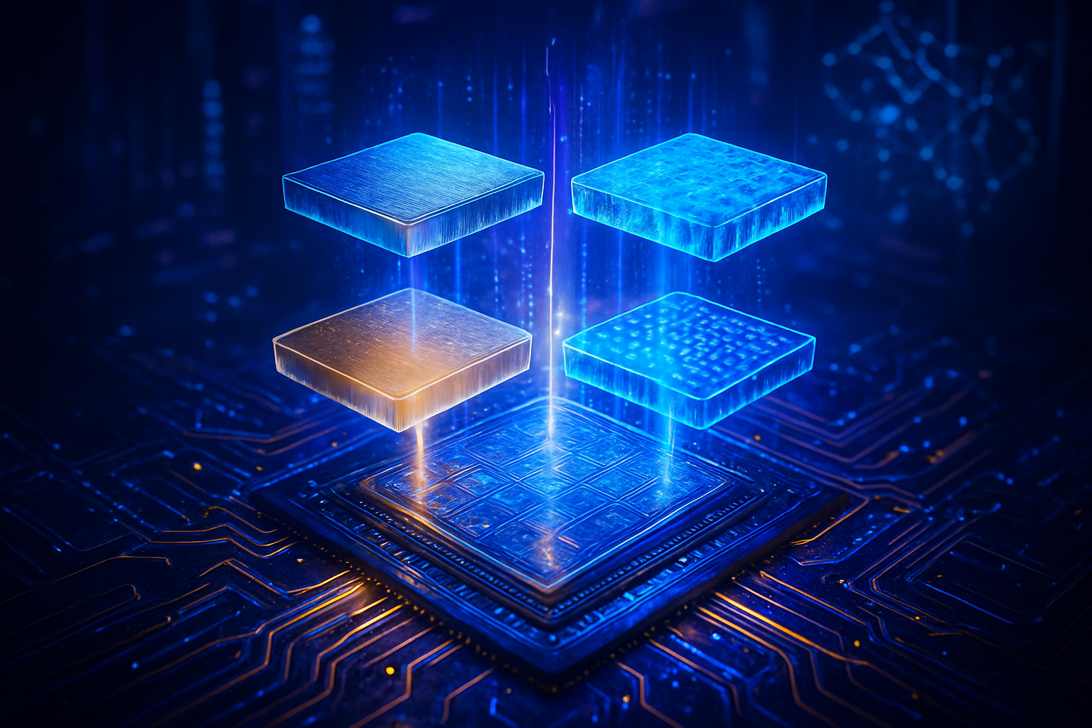
    The current shortage is primarily fueled by the rapid transition from HBM3E to the upcoming HBM4 standard. While HBM3E is the current workhorse for NVIDIA (NASDAQ: NVDA) H200 and Blackwell GPUs, HBM4 represents a massive architectural leap. Technical specifications for HBM4 include a doubling of the memory interface from 1024-bit to 2048-bit, enabling bandwidth speeds of up to 2.8 TB/s per stack. This evolution is necessary to feed the massive data requirements of trillion-parameter models, but it comes at a significant cost to production efficiency.

    Manufacturing HBM4 is exponentially more complex than standard DDR5 memory. The process requires advanced Through-Silicon Via (TSV) stacking and, for the first time, utilizes foundry-level logic processes for the base die. Because HBM requires roughly twice the wafer area of standard DRAM for the same number of bits, and current yields are hovering between 50% and 60%, every AI-grade chip produced effectively "cannibalizes" the capacity of three to four standard PC RAM chips. This technical bottleneck is the primary engine driving the 171.8% year-over-year price surge observed in late 2025.

    Industry experts and researchers at firms like TrendForce note that this is a departure from previous cycles where oversupply eventually corrected prices. Instead, the complexity of HBM4 production has created a "yield wall." Even as manufacturers like Micron Technology (NASDAQ: MU) attempt to scale, the physical limitations of stacking 12 and 16 layers of DRAM with precision are keeping supply tight and prices at record highs.

    Market Upheaval: SK Hynix Challenges the Throne

    The AI boom has upended the traditional hierarchy of the memory market. For the first time in nearly 40 years, Samsung’s undisputed lead in memory revenue was successfully challenged by SK Hynix in early 2025. By leveraging its "first-mover" advantage and a tight partnership with NVIDIA, SK Hynix has captured approximately 60% of the HBM market share. Although Samsung has recently cleared technical hurdles for its 12-layer HBM3E and begun volume shipments to reclaim some ground, the race for dominance in the HBM4 era remains a dead heat.

    This competition is forcing strategic shifts across the board. Micron Technology recently made the drastic decision to wind down its famous "Crucial" consumer brand, signaling a total exit from the DIY PC RAM market to focus exclusively on high-margin enterprise AI and automotive sectors. Meanwhile, tech giants like OpenAI are moving to secure their own futures; reports indicate a landmark deal where OpenAI has secured long-term supply agreements for nearly 40% of global DRAM wafer output through 2029 to support its massive "Stargate" data center initiative.

    For AI labs and tech giants, memory has become the new "oil." Companies that failed to secure long-term HBM contracts in 2024 are now finding themselves priced out of the market or facing lead times that stretch into 2027. This has created a strategic advantage for well-capitalized firms that can afford to subsidize the skyrocketing costs of memory to maintain their lead in the AI arms race.

    A Wider Crisis for the Global Tech Landscape

    The implications of this shortage extend far beyond the walls of data centers. As manufacturers pivot 40% of their wafer capacity to HBM, the supply of "commodity" DRAM—the memory found in laptops, smartphones, and home appliances—has been severely rationed. Major PC manufacturers like Dell (NYSE: DELL) and Lenovo have already begun hiking system prices by 15% to 20% to offset these costs, reversing a decade-long trend of falling memory prices for consumers.

    This structural shift mirrors previous silicon shortages, such as the 2020-2022 automotive chip crisis, but with a more permanent outlook. The "memory super-cycle" is not just a temporary spike; it represents a fundamental change in how silicon is valued. Memory is no longer a cheap, interchangeable commodity but a high-performance logic component. There are growing concerns that this "AI tax" on memory will lead to a contraction in the global PC market, as entry-level devices are forced to ship with inadequate RAM to remain affordable.

    Furthermore, the concentration of memory production into AI-focused high-margin products raises geopolitical concerns. With the majority of HBM production concentrated in South Korea and a significant portion of the supply pre-sold to a handful of American tech giants, smaller nations and industries are finding themselves at the bottom of the priority list for essential computing components.

    The Road to 2026: What Lies Ahead

    Looking toward the near future, the industry is bracing for an even tighter squeeze. Both SK Hynix and Samsung have reportedly accelerated their HBM4 production schedules, moving mass production forward to February 2026 to meet the demands of NVIDIA’s "Rubin" architecture. Analysts project that DRAM prices will rise an additional 40% to 50% through the first half of 2026 before any potential plateau is reached.

    The next frontier in this evolution is "Custom HBM." In late 2026 and 2027, we expect to see the first memory stacks where the logic die is custom-built for specific AI chips, such as those from Amazon (NASDAQ: AMZN) or Google (NASDAQ: GOOGL). This will further complicate the manufacturing process, making memory even more of a specialized, high-cost component. Relief is not expected until 2027, when new mega-fabs like Samsung’s P4L and SK Hynix’s M15X reach volume production.

    The primary challenge for the industry will be balancing this AI gold rush with the needs of the broader electronics ecosystem. If the shortage of commodity DRAM becomes too severe, it could stifle innovation in other sectors, such as edge computing and the Internet of Things (IoT), which rely on cheap, abundant memory to function.

    Final Assessment: A Permanent Shift in Computing

    The current AI-driven DRAM shortage marks a turning point in the history of computing. We are witnessing the end of the era of "cheap memory" and the beginning of a period where the ability to store and move data is as valuable—and as scarce—as the ability to process it. The pivot to HBM4 is not just a technical upgrade; it is a declaration that the future of the semiconductor industry is inextricably linked to the trajectory of artificial intelligence.

    In the coming weeks and months, market watchers should keep a close eye on the yield rates of HBM4 pilot lines and the quarterly earnings of PC OEMs. If yield rates fail to improve, the 2026 price peak could be even higher than currently forecasted. For now, the "memory super-cycle" shows no signs of slowing down, and its impact will be felt in every corner of the technology world for years to come.


    This content is intended for informational purposes only and represents analysis of current AI developments.

    TokenRing AI delivers enterprise-grade solutions for multi-agent AI workflow orchestration, AI-powered development tools, and seamless remote collaboration platforms.
    For more information, visit https://www.tokenring.ai/.

  • High-NA EUV Era Begins: Intel Deploys First ASML Tool as China Signals EUV Prototype Breakthrough

    High-NA EUV Era Begins: Intel Deploys First ASML Tool as China Signals EUV Prototype Breakthrough

    The global semiconductor landscape reached a historic inflection point in late 2025 as Intel Corporation (NASDAQ: INTC) announced the successful installation and acceptance testing of the industry's first commercial High-Numerical Aperture (High-NA) Extreme Ultraviolet (EUV) lithography tool. The machine, a $350 million ASML (NASDAQ: ASML) Twinscan EXE:5200B, represents the most advanced piece of manufacturing equipment ever created, signaling the start of the "Angstrom Era" in chip production. By securing the first of these massive systems, Intel aims to leapfrog its rivals and reclaim the crown of transistor density and power efficiency.

    However, the Western technological lead is facing an unprecedented challenge from the East. Simultaneously, reports have emerged from Shenzhen, China, indicating that a domestic research consortium has validated a working EUV prototype. This breakthrough, part of a state-sponsored "Manhattan Project" for semiconductors, suggests that China is making rapid progress in bypassing US-led export bans. While the Chinese prototype is not yet ready for high-volume manufacturing, its existence marks a significant milestone in Beijing’s quest for technological sovereignty, with a stated goal of producing domestic EUV-based processors by 2028.

    The Technical Frontier: 1.4nm and the High-NA Advantage

    The ASML Twinscan EXE:5200B is a marvel of engineering, standing nearly two stories tall and requiring multiple Boeing 747s for transport. The defining feature of this tool is its Numerical Aperture (NA), which has been increased from the 0.33 of standard EUV machines to 0.55. This jump in NA allows for an 8nm resolution, a significant improvement over the 13.5nm limit of previous generations. For Intel, this means the ability to print features for its upcoming 14A (1.4nm) node using "single-patterning." Previously, achieving such small dimensions required "multi-patterning," a process where a single layer is printed multiple times, which increases the risk of defects and dramatically raises production costs.

    Initial reactions from the semiconductor research community have been a mix of awe and cautious optimism. Dr. Aris Silzars, a veteran industry analyst, noted that the EXE:5200B’s throughput—capable of processing 175 to 200 wafers per hour—is the "holy grail" for making the 1.4nm node economically viable. The tool also boasts an overlay accuracy of 0.7 nanometers, a precision equivalent to hitting a golf ball on the moon from Earth. Experts suggest that by adopting High-NA early, Intel is effectively "de-risking" its roadmap for the next decade, while competitors like Taiwan Semiconductor Manufacturing Company (NYSE: TSM) and Samsung Electronics (KRX: 005930) have opted for a more conservative approach, extending the life of standard EUV tools through complex multi-patterning techniques.

    In contrast, the Chinese prototype developed in Shenzhen utilizes a different technical path. While ASML uses Laser-Produced Plasma (LPP) to generate EUV light, the Chinese team, reportedly led by engineers from Huawei and various state-funded institutes, has successfully demonstrated a Laser-Induced Discharge Plasma (LDP) source. Though currently producing only 100W–150W of power—roughly half of what is needed for high-speed commercial production—it proves that China has solved the fundamental physics of EUV light generation. This "Manhattan Project" approach has involved a massive mobilization of talent, including former ASML and Nikon (OTC: NINNY) engineers, to reverse-engineer the complex reflective optics and light sources that were previously thought to be decades out of reach for domestic Chinese firms.

    Strategic Maneuvers: The Battle for Lithography Leadership

    Intel’s aggressive move to install the EXE:5200B is a clear strategic play to regain the manufacturing lead it lost over the last decade. By being the first to master High-NA, Intel (NASDAQ: INTC) provides its foundry customers with a unique value proposition: the ability to manufacture the world’s most advanced AI and mobile chips with fewer processing steps and higher yields. This development puts immense pressure on TSMC (NYSE: TSM), which has dominated the 3nm and 5nm markets. If Intel can successfully ramp up the 14A node by 2026 or 2027, it could disrupt the current foundry hierarchy and attract major clients like Apple and Nvidia that have traditionally relied on Taiwanese fabrication.

    The competitive implications extend far beyond the United States and Taiwan. China's breakthrough in Shenzhen represents a direct challenge to the efficacy of the U.S. Department of Commerce's export controls. For years, the denial of EUV tools to Chinese firms like SMIC was considered a "hard ceiling" that would prevent China from progressing beyond the 7nm or 5nm nodes. The validation of a domestic EUV prototype suggests that this ceiling is cracking. If China can scale this technology, it would not only secure its own supply chain but also potentially offer a cheaper, state-subsidized alternative to the global market, disrupting the high-margin business models of Western equipment makers.

    Furthermore, the emergence of the Chinese "Manhattan Project" has sparked a new arms race in lithography. Companies like Canon (NYSE: CAJ) are attempting to bypass EUV altogether with "nanoimprint" lithography, but the industry consensus remains that EUV is the only viable path for sub-2nm chips. Intel’s first-mover advantage with the EXE:5200B creates a "financial and technical moat" that may be too expensive for smaller players to cross, potentially consolidating the leading-edge market into a triopoly of Intel, TSMC, and Samsung.

    Geopolitical Stakes and the Future of Moore’s Law

    The simultaneous announcements from Oregon and Shenzhen highlight the intensifying "Chip War" between the U.S. and China. This is no longer just a corporate competition; it is a matter of national security and economic survival. The High-NA EUV tools are the "printing presses" of the modern era, and the nation that controls them controls the future of Artificial Intelligence, autonomous systems, and advanced weaponry. Intel's success is seen as a validation of the CHIPS Act and the U.S. strategy to reshore critical manufacturing.

    However, the broader AI landscape is also at stake. As AI models grow in complexity, the demand for more transistors per square millimeter becomes insatiable. High-NA EUV is the only technology currently capable of sustaining the pace of Moore’s Law—the observation that the number of transistors on a microchip doubles about every two years. Without the precision of the EXE:5200B, the industry would likely face a "performance wall," where the energy costs of running massive AI data centers would become unsustainable.

    The potential concerns surrounding this development are primarily geopolitical. If China succeeds in its 2028 goal of domestic EUV processors, it could render current sanctions obsolete and lead to a bifurcated global tech ecosystem. We are witnessing the end of a globalized semiconductor supply chain and the birth of two distinct, competing stacks: one led by the U.S. and ASML, and another led by China’s centralized "whole-of-nation" effort. This fragmentation could lead to higher costs for consumers and a slower pace of global innovation as research is increasingly siloed behind national borders.

    The Road to 2028: What Lies Ahead

    Looking forward, the next 24 to 36 months will be critical for both Intel and the Chinese consortium. For Intel (NASDAQ: INTC), the challenge is transitioning from "installation" to "yield." It is one thing to have a $350 million machine; it is another to produce millions of perfect chips with it. The industry will be watching closely for the first "tape-outs" of the 14A node, which will serve as the litmus test for High-NA's commercial viability. If Intel can prove that High-NA reduces the total cost of ownership per transistor, it will have successfully executed one of the greatest comebacks in industrial history.

    In China, the focus will shift from the Shenzhen prototype to the more ambitious "Steady-State Micro-Bunching" (SSMB) project in Xiong'an. Unlike the standalone ASML tools, SSMB uses a particle accelerator to generate EUV light for an entire cluster of lithography machines. If this centralized light-source model works, it could fundamentally change the economics of chipmaking, allowing China to build "EUV factories" that are more scalable than anything in the West. Experts predict that while 2028 is an aggressive target for domestic EUV processors, a 2030 timeline for stable production is increasingly realistic.

    The immediate challenges remain daunting. For Intel, the "reticle stitching" required by High-NA’s smaller field size presents a significant software and design hurdle. For China, the lack of a mature ecosystem for EUV photoresists and masks—the specialized chemicals and plates used in the printing process—could still stall their progress even if the light source is perfected. The race is now a marathon of engineering endurance.

    Conclusion: A New Chapter in Silicon History

    The installation of the ASML Twinscan EXE:5200B at Intel and the emergence of China’s EUV prototype represent the start of a new chapter in silicon history. We have officially moved beyond the era where 0.33 NA lithography was the pinnacle of human achievement. The "High-NA Era" promises to push computing power to levels previously thought impossible, enabling the next generation of AI breakthroughs that will define the late 2020s and beyond.

    As we move into 2026, the significance of these developments cannot be overstated. Intel has reclaimed a seat at the head of the technical table, but China has proven that it will not be easily sidelined. The "Manhattan Project" for chips is no longer a theoretical threat; it is a functional reality that is beginning to produce results. The long-term impact will be a world where the most advanced technology is both a tool for incredible progress and a primary instrument of geopolitical power.

    In the coming weeks and months, industry watchers should look for announcements regarding Intel's first 14A test chips and any further technical disclosures from the Shenzhen research group. The battle for the 1.4nm node has begun, and the stakes have never been higher.


    This content is intended for informational purposes only and represents analysis of current AI developments.

    TokenRing AI delivers enterprise-grade solutions for multi-agent AI workflow orchestration, AI-powered development tools, and seamless remote collaboration platforms.
    For more information, visit https://www.tokenring.ai/.

  • NVIDIA Reports Record $51.2B Q3 Revenue as Blackwell Demand Hits ‘Insane’ Levels

    NVIDIA Reports Record $51.2B Q3 Revenue as Blackwell Demand Hits ‘Insane’ Levels

    In a financial performance that has effectively silenced skeptics of the "AI bubble," NVIDIA Corporation (NASDAQ: NVDA) has once again shattered industry expectations. The company reported record-breaking Q3 FY2026 revenue of $51.2 billion for its Data Center segment alone, contributing to a total quarterly revenue of $57.0 billion—a staggering 66% year-on-year increase. This explosive growth is being fueled by the rapid transition to the Blackwell architecture, which CEO Jensen Huang described during the earnings call as seeing demand that is "off the charts" and "insane."

    The implications of these results extend far beyond a single balance sheet; they signal a fundamental shift in the global computing landscape. As traditional data centers are being decommissioned in favor of "AI Factories," NVIDIA has positioned itself as the primary architect of this new industrial era. With a production ramp-up that is the fastest in semiconductor history, the company is now shipping approximately 1,000 GB200 NVL72 liquid-cooled racks every week. These systems are the backbone of massive-scale projects like xAI’s Colossus 2, marking a new era of compute density that was unthinkable just eighteen months ago.

    The Blackwell Breakthrough: Engineering the AI Factory

    At the heart of NVIDIA's dominance is the Blackwell B200 and GB200 series, a platform that represents a quantum leap over the previous Hopper generation. The flagship GB200 NVL72 is not merely a chip but a massive, unified system that acts as a single GPU. Each rack contains 72 Blackwell GPUs and 36 Grace CPUs, interconnected via NVIDIA’s fifth-generation NVLink. This architecture delivers up to a 30x increase in inference performance and a 25x increase in energy efficiency for trillion-parameter models compared to the H100. This efficiency is critical as the industry shifts from training static models to deploying real-time, autonomous AI agents.

    The technical complexity of these systems has necessitated a revolution in data center design. To manage the immense heat generated by Blackwell’s 1,200W TDP (Thermal Design Power), NVIDIA has moved toward a liquid-cooled standard. The 1,000 racks shipping weekly are complex machines comprising over 600,000 individual components, requiring a sophisticated global supply chain that competitors are struggling to replicate. Initial reactions from the AI research community have been overwhelmingly positive, with engineers noting that the Blackwell interconnect bandwidth allows for the training of models with context windows previously deemed computationally impossible.

    A Widening Moat: Industry Impact and Competitive Pressure

    The sheer scale of NVIDIA's Q3 results has sent ripples through the "Magnificent Seven" and the broader tech sector. While competitors like Advanced Micro Devices, Inc. (NASDAQ: AMD) have made strides with their MI325 and MI350 series, NVIDIA’s 73-76% gross margins suggest a level of pricing power that remains unchallenged. Major Cloud Service Providers (CSPs) including Microsoft Corporation (NASDAQ: MSFT), Alphabet Inc. (NASDAQ: GOOGL), and Amazon.com, Inc. (NASDAQ: AMZN) continue to be NVIDIA’s largest customers, even as they develop their own internal silicon like Google’s TPU and Amazon’s Trainium.

    The strategic advantage for these tech giants lies in the "CUDA Moat." NVIDIA’s software ecosystem, refined over two decades, remains the industry standard for AI development. For startups and enterprise giants alike, the cost of switching away from CUDA—which involves rewriting entire software stacks and optimizing for less mature hardware—often outweighs the potential savings of cheaper chips. Furthermore, the rise of "Physical AI" and robotics has given NVIDIA a new frontier; its Omniverse platform and Jetson Thor chips are becoming the foundational layers for the next generation of autonomous machines, a market where its competitors have yet to establish a significant foothold.

    Scaling Laws vs. Efficiency: The Broader AI Landscape

    Despite the record revenue, NVIDIA’s report comes at a time of intense debate regarding the "AI Bubble." Critics point to the massive capital expenditures of hyperscalers—estimated to exceed $250 billion collectively in 2025—and question the ultimate return on investment. The late 2025 "DeepSeek Shock," where a Chinese startup demonstrated high-performance model training at a fraction of the cost of U.S. counterparts, has raised questions about whether "brute force" scaling is reaching a point of diminishing returns.

    However, NVIDIA has countered these concerns by pivoting the narrative toward "Infrastructure Economics." Jensen Huang argues that the cost of not building AI infrastructure is higher than the cost of the hardware itself, as AI-driven productivity gains begin to manifest in software services. NVIDIA’s networking segment, which saw revenue hit $8.2 billion this quarter, underscores this trend. The shift from InfiniBand to Spectrum-X Ethernet is allowing more enterprises to build private AI clouds, democratizing access to high-end compute and moving the industry away from a total reliance on the largest hyperscalers.

    The Road to Rubin: Future Developments and the Next Frontier

    Looking ahead, NVIDIA has already provided a glimpse into the post-Blackwell era. The company confirmed that its next-generation Rubin architecture (R100) has successfully "taped out" and is on track for a 2026 launch. Rubin will feature HBM4 memory and the new Vera CPU, specifically designed to handle "Agentic Inference"—the process of AI models making complex, multi-step decisions in real-time. This shift from simple chatbots to autonomous digital workers is expected to drive the next massive wave of demand.

    Challenges remain, particularly in the realm of power and logistics. The expansion of xAI’s Colossus 2 project in Memphis, which aims for a cluster of 1 million GPUs, has already faced hurdles related to local power grid stability and environmental impact. NVIDIA is addressing these issues by collaborating with energy providers on modular, nuclear-powered data centers and advanced liquid-cooling substations. Experts predict that the next twelve months will be defined by "Physical AI," where NVIDIA's hardware moves out of the data center and into the real world via humanoid robots and autonomous industrial systems.

    Conclusion: The Architect of the Intelligence Age

    NVIDIA’s Q3 FY2026 earnings report is more than a financial milestone; it is a confirmation that the AI revolution is accelerating rather than slowing down. By delivering record revenue and maintaining nearly 75% margins while shipping massive-scale liquid-cooled systems at a weekly cadence, NVIDIA has solidified its role as the indispensable provider of the world's most valuable resource: compute.

    As we move into 2026, the industry will be watching closely to see if the massive CapEx from hyperscalers translates into sustainable software revenue. While the "bubble" debate will undoubtedly continue, NVIDIA’s relentless innovation cycle—moving from Blackwell to Rubin at breakneck speed—ensures that it remains several steps ahead of any potential market correction. For now, the "AI Factory" is running at full capacity, and the world is only beginning to see the products it will create.


    This content is intended for informational purposes only and represents analysis of current AI developments.

    TokenRing AI delivers enterprise-grade solutions for multi-agent AI workflow orchestration, AI-powered development tools, and seamless remote collaboration platforms.
    For more information, visit https://www.tokenring.ai/.

  • Global Semiconductor Market Set to Hit $1 Trillion by 2026 Driven by AI Super-Cycle

    Global Semiconductor Market Set to Hit $1 Trillion by 2026 Driven by AI Super-Cycle

    As 2025 draws to a close, the technology sector is bracing for a historic milestone. Bank of America (NYSE: BAC) analyst Vivek Arya has issued a landmark projection stating that the global semiconductor market is on a collision course with the $1 trillion mark by 2026. Driven by what Arya describes as a "once-in-a-generation" AI super-cycle, the industry is expected to see a massive 30% year-on-year increase in sales, fueled by the aggressive infrastructure build-out of the world’s largest technology companies.

    This surge is not merely a continuation of current trends but represents a fundamental shift in the global computing landscape. As artificial intelligence moves from the experimental training phase into high-volume, real-time inference, the demand for specialized accelerators and next-generation memory has reached a fever pitch. With hyperscalers like Microsoft (NASDAQ: MSFT), Alphabet (NASDAQ: GOOGL), and Meta (NASDAQ: META) committing hundreds of billions in capital expenditure, the semiconductor industry is entering its most significant strategic transformation in over a decade.

    The Technical Engine: From Training to Inference and the Rise of HBM4

    The projected $1 trillion milestone is underpinned by a critical technical evolution: the transition from AI training to high-scale inference. While the last three years were dominated by the massive compute power required to train frontier models, 2026 is set to be the year of "inference at scale." This shift requires a different class of hardware—one that prioritizes memory bandwidth and energy efficiency over raw floating-point operations.

    Central to this transition is the arrival of High Bandwidth Memory 4 (HBM4). Unlike its predecessors, HBM4 features a 2,048-bit physical interface—double that of HBM3e—enabling bandwidth speeds of up to 2.0 TB/s per stack. This leap is essential for solving the "memory wall" that has long bottlenecked trillion-parameter models. By integrating custom logic dies directly into the memory stack, manufacturers like Micron (NASDAQ: MU) and SK Hynix are enabling "Thinking Models" to reason through complex queries in real-time, significantly reducing the "time-to-first-token" for end-users.

    Industry experts and the AI research community have noted that this shift is also driving a move toward "disaggregated prefill-decode" architectures. By separating the initial processing of a prompt from the iterative generation of a response, 2026-era accelerators can achieve up to a 40% improvement in power efficiency. This technical refinement is crucial as data centers begin to hit the physical limits of power grids, making performance-per-watt the most critical metric for the coming year.

    The Beneficiaries: NVIDIA and Broadcom Lead the "Brain and Nervous System"

    The primary beneficiaries of this $1 trillion expansion are NVIDIA (NASDAQ: NVDA) and Broadcom (NASDAQ: AVGO). Vivek Arya’s report characterizes NVIDIA as the "Brain" of the AI revolution, while Broadcom serves as its "Nervous System." NVIDIA’s upcoming Rubin (R100) architecture, slated for late 2026, is expected to leverage HBM4 and a 3nm manufacturing process to provide a 3x performance leap over the current Blackwell generation. With visibility into over $500 billion in demand, NVIDIA remains in a "different galaxy" compared to its competitors.

    Broadcom, meanwhile, has solidified its position as the cornerstone of custom AI infrastructure. As hyperscalers seek to reduce their total cost of ownership (TCO), they are increasingly turning to Broadcom for custom Application-Specific Integrated Circuits (ASICs). These chips, such as Google’s TPU v7 and Meta’s MTIA v3, are stripped of general-purpose legacy features, allowing them to run specific AI workloads at a fraction of the power cost of general GPUs. This strategic advantage has made Broadcom indispensable for the networking and custom silicon needs of the world’s largest data centers.

    The competitive implications are stark. While major AI labs like OpenAI and Anthropic continue to push the boundaries of model intelligence, the underlying "arms race" is being won by the companies providing the picks and shovels. Tech giants are now engaged in "offensive and defensive" spending; they must invest to capture new AI markets while simultaneously spending to protect their existing search, social media, and cloud empires from disruption.

    Wider Significance: A Decade-Long Structural Transformation

    This "AI Super-Cycle" is being compared to the internet boom of the 1990s and the mobile revolution of the 2000s, but with a significantly faster velocity. Arya argues that we are only three years into an 8-to-10-year journey, dismissing concerns of a short-term bubble. The "flywheel effect"—where massive CapEx creates intelligence, which is then monetized to fund further infrastructure—is now in full motion.

    However, the scale of this growth brings significant concerns regarding energy consumption and sovereign AI. As nations realize that AI compute is a matter of national security, we are seeing the rise of "Inference Factories" built within national borders to ensure data privacy and energy independence. This geopolitical dimension adds another layer of demand to the semiconductor market, as countries like Japan, France, and the UK look to build their own sovereign AI clusters using chips from NVIDIA and equipment from providers like Lam Research (NASDAQ: LRCX) and KLA Corp (NASDAQ: KLAC).

    Compared to previous milestones, the $1 trillion mark represents more than just a financial figure; it signifies the moment semiconductors became the primary driver of the global economy. The industry is no longer cyclical in the traditional sense, tied to consumer electronics or PC sales; it is now a foundational utility for the age of artificial intelligence.

    Future Outlook: The Path to $1.2 Trillion and Beyond

    Looking ahead, the momentum is expected to carry the market well past the $1 trillion mark. By 2030, the Total Addressable Market (TAM) for AI data center systems is projected to exceed $1.2 trillion, with AI accelerators alone representing a $900 billion opportunity. In the near term, we expect to see a surge in "Agentic AI," where HBM4-powered cloud servers handle complex reasoning while edge devices, powered by chips from Analog Devices (NASDAQ: ADI) and designed with software from Cadence Design Systems (NASDAQ: CDNS), handle local interactions.

    The primary challenges remaining are yield management and the physical limits of semiconductor fabrication. As the industry moves to 2nm and beyond, the cost of manufacturing equipment will continue to rise, potentially consolidating power among a handful of "mega-fabs." Experts predict that the next phase of the cycle will focus on "Test-Time Compute," where models use more processing power during the query phase to "think" through problems, further cementing the need for the massive infrastructure currently being deployed.

    Summary and Final Thoughts

    The projection of a $1 trillion semiconductor market by 2026 is a testament to the unprecedented scale of the AI revolution. Driven by a 30% YoY growth surge and the strategic shift toward inference, the industry is being reshaped by the massive CapEx of hyperscalers and the technical breakthroughs in HBM4 and custom silicon. NVIDIA and Broadcom stand at the apex of this transformation, providing the essential components for a new era of accelerated computing.

    As we move into 2026, the key metrics to watch will be the "cost-per-token" of AI models and the ability of power grids to keep pace with data center expansion. This development is not just a milestone for the tech industry; it is a defining moment in AI history that will dictate the economic and geopolitical landscape for the next decade.


    This content is intended for informational purposes only and represents analysis of current AI developments.

    TokenRing AI delivers enterprise-grade solutions for multi-agent AI workflow orchestration, AI-powered development tools, and seamless remote collaboration platforms.
    For more information, visit https://www.tokenring.ai/.

  • Grasshopper Bank Becomes First Community Bank to Launch Conversational AI Financial Analysis via Anthropic’s MCP

    Grasshopper Bank Becomes First Community Bank to Launch Conversational AI Financial Analysis via Anthropic’s MCP

    In a significant leap for the democratization of high-end financial technology, Grasshopper Bank has officially become the first community bank in the United States to integrate Anthropic’s Model Context Protocol (MCP). This move allows the bank’s business clients to perform complex, natural language financial analysis directly through AI assistants like Claude. By bridging the gap between live banking data and large language models (LLMs), Grasshopper is transforming the traditional banking dashboard into a conversational partner capable of real-time cash flow analysis and predictive modeling.

    The announcement, which saw its initial rollout in August 2025 and has since expanded to include multi-model support, represents a pivotal shift in how small-to-medium businesses (SMBs) interact with their capital. Developed in partnership with the digital banking platform Narmi, the integration utilizes a secure, read-only data bridge that empowers founders and CFOs to ask nuanced questions about their finances without the need for manual data exports or complex spreadsheet formulas. This development marks a milestone in the "agentic" era of banking, where AI does not just display data but understands and interprets it in context.

    The Technical Architecture: Beyond RAG and Traditional APIs

    The core of this innovation lies in the Model Context Protocol (MCP), an open-source standard pioneered by Anthropic to solve the "integration tax" that has long plagued AI development. Historically, connecting an AI to a specific data source required bespoke, brittle API integrations. MCP replaces this with a universal client-server architecture, often described as the "USB-C port for AI." Grasshopper’s implementation utilizes a custom MCP server built by Narmi, which acts as a secure gateway. When a client asks a question, the AI "host" (such as Claude) communicates with the MCP server using JSON-RPC 2.0, discovering available "Tools" and "Resources" at runtime.

    Unlike traditional Retrieval-Augmented Generation (RAG), which often involves pre-indexing data into a vector database, the MCP approach is dynamic and "surgical." Instead of flooding the AI’s context window with potentially irrelevant chunks of transaction history, the AI uses specific MCP tools to query only the necessary data points—such as a specific month’s SaaS spend or a vendor's payment history—based on its own reasoning. This reduces latency and significantly improves the accuracy of the financial insights provided. The system is built on a "read-only" architecture, ensuring that while the AI can analyze data, it cannot initiate transactions or move funds, maintaining a strict security perimeter.

    Furthermore, the implementation utilizes OAuth 2.1 for permissioned access, meaning the AI assistant never sees or stores a user’s banking credentials. The technical achievement here is not just the connection itself, but the standardization of it. By adopting MCP, Grasshopper has avoided the "walled garden" approach of proprietary AI systems. This allows the bank to remain model-agnostic; while the service launched with Anthropic’s Claude, it has already expanded to support OpenAI’s ChatGPT and is slated to integrate Google’s Gemini, a product of Alphabet (NASDAQ: GOOGL), by early 2026.

    Leveling the Playing Field: Strategic Implications for the Banking Sector

    The adoption of MCP by a community bank with approximately $1.4 billion in assets sends a clear message to the "Too Big to Fail" institutions. Traditionally, advanced AI-driven financial insights were the exclusive domain of giants like JPMorgan Chase or Bank of America, who possess the multi-billion dollar R&D budgets required to build in-house proprietary models. By leveraging an open-source protocol and partnering with a nimble FinTech like Narmi, Grasshopper has bypassed years of development, effectively "leapfrogging" the traditional innovation cycle.

    This development poses a direct threat to the competitive advantage of larger banks' proprietary "digital assistants." As more community banks adopt open standards like MCP, the "sticky" nature of big-bank ecosystems may begin to erode. Startups and SMBs, who often prefer the personalized service of a community bank but require the high-tech tools of a global firm, no longer have to choose between the two. This shift could trigger a wave of consolidation in the FinTech space, as providers who do not support open AI protocols find themselves locked out of an increasingly interconnected financial web.

    Moreover, the strategic partnership between Anthropic and Amazon (NASDAQ: AMZN), which has seen billions in investment, provides a robust cloud infrastructure that ensures these MCP-driven services can scale rapidly. As Microsoft (NASDAQ: MSFT) continues to push its own AI "Copilots" into the enterprise space, the move by Grasshopper to support multiple models ensures they are not beholden to a single tech giant’s roadmap. This "Switzerland-style" neutrality in model support is likely to become a preferred strategy for regional banks looking to maintain autonomy while offering cutting-edge features.

    The Broader AI Landscape: From Chatbots to Financial Agents

    The significance of Grasshopper’s move extends far beyond the balance sheet of a single bank; it signals a transition in the broader AI landscape from "chatbots" to "agents." In the previous era of AI, users were responsible for bringing data to the model. In this new era, the model is securely brought to the data. This integration is a prime example of "Agentic Banking," where the AI is granted a persistent, contextual understanding of a user’s financial life. This mirrors trends seen in other sectors, such as AI-powered IDEs for software development or autonomous research agents in healthcare.

    However, the democratization of such powerful tools does not come without concerns. While the current read-only nature of the Grasshopper integration mitigates immediate risks of unauthorized fund transfers, the potential for "hallucinated" financial advice remains a hurdle. If an AI incorrectly categorizes a major expense or miscalculates a burn rate, the consequences for a small business could be severe. This highlights the ongoing need for "Human-in-the-Loop" systems, where the AI provides the analysis but the human CFO makes the final decision.

    Comparatively, this milestone is being viewed by industry experts as the "Open Banking 2.0" moment. Where the first wave of open banking focused on the portability of data via APIs (facilitated by companies like Plaid), this second wave is about the interpretability of that data. The ability for a business owner to ask, "Will I have enough cash to hire a new engineer in October?" and receive a data-backed response in seconds is a fundamental shift in the utility of financial services.

    The Road Ahead: Autonomous Banking and Write-Access

    Looking toward 2026, the roadmap for MCP in banking is expected to move from "read" to "write." While Grasshopper has started with read-only analysis to ensure safety, the next logical step is the integration of "Action Tools" within the MCP framework. This would allow an AI assistant to not only identify an upcoming bill but also draft the payment for the user to approve with a single click. Experts predict that "Autonomous Treasury Management" will become a standard offering for SMBs, where AI agents automatically move funds between high-yield savings and operating accounts to maximize interest while ensuring liquidity.

    The near-term developments will likely focus on expanding the "context" the AI can access. This could include integrating with accounting software like QuickBooks or tax filing services, allowing the AI to provide a truly holistic view of a company’s financial health. The challenge will remain the standardization of these connections; if every bank and software provider uses a different protocol, the vision of a seamless AI agent falls apart. Grasshopper’s early bet on MCP is a gamble that Anthropic’s standard will become the industry’s "lingua franca."

    Final Reflections: A New Era for Financial Intelligence

    Grasshopper Bank’s integration of the Model Context Protocol is more than just a new feature; it is a blueprint for the future of community banking. By proving that a smaller institution can deliver world-class AI capabilities through open standards, Grasshopper has set a precedent that will likely be followed by hundreds of other regional banks in the coming months. The era of the static bank statement is ending, replaced by a dynamic, conversational interface that puts the power of a full-time financial analyst into the pocket of every small business owner.

    In the history of AI development, 2025 may well be remembered as the year that protocols like MCP finally allowed LLMs to "touch" the real world in a secure and scalable way. As we move into 2026, the industry will be watching closely to see how users adopt these tools and how "Big Tech" responds to the encroachment of open-standard AI into their once-proprietary domains. For now, Grasshopper Bank stands at the forefront of a movement that is making financial intelligence more accessible, transparent, and actionable than ever before.


    This content is intended for informational purposes only and represents analysis of current AI developments.

    TokenRing AI delivers enterprise-grade solutions for multi-agent AI workflow orchestration, AI-powered development tools, and seamless remote collaboration platforms.
    For more information, visit https://www.tokenring.ai/.

  • The Agentic Revolution: How Siri 2.0 and the iPhone 17 Are Redefining the Smartphone Era

    The Agentic Revolution: How Siri 2.0 and the iPhone 17 Are Redefining the Smartphone Era

    As of late 2025, the smartphone is no longer just a portal to apps; it has become an autonomous digital executive. With the wide release of Siri 2.0 and the flagship iPhone 17 lineup, Apple (NASDAQ:AAPL) has successfully transitioned its iconic virtual assistant from a reactive voice-interface into a proactive "agentic" powerhouse. This shift, powered by the Apple Intelligence 2.0 suite, has not only silenced critics of Apple’s perceived "AI lag" but has also ignited what analysts are calling the "AI Supercycle," driving record-breaking hardware sales and fundamentally altering the relationship between users and their devices.

    The immediate significance of Siri 2.0 lies in its ability to understand intent rather than just commands. By combining deep on-screen awareness with a cross-app action framework, Siri can now execute complex, multi-step workflows that previously required minutes of manual navigation. Whether it is retrieving a specific document from a buried email thread to summarize and Slack it to a colleague, or identifying a product on a social media feed and adding it to a shopping list, the "agentic" Siri operates with a level of autonomy that makes the traditional "App Store" model feel like a relic of the past.

    The Technical Architecture of Autonomy

    Technically, Siri 2.0 represents a total overhaul of the Apple Intelligence framework. At its core is the Semantic Index, an on-device map of a user’s entire digital life—spanning Messages, Mail, Calendar, and Photos. Unlike previous versions of Siri that relied on hardcoded intent-matching, Siri 2.0 utilizes a generative reasoning engine capable of "planning." When a user gives a complex instruction, the system breaks it down into sub-tasks, identifying which apps contain the necessary data and which APIs are required to execute the final action.

    This leap in capability is supported by the A19 Pro silicon, manufactured on TSMC’s (NYSE:TSM) advanced 3nm (N3P) process. The chip features a redesigned 16-core Neural Engine specifically optimized for 3-billion-parameter local Large Language Models (LLMs). To support these memory-intensive tasks, Apple has increased the baseline RAM for the iPhone 17 Pro and the new "iPhone Air" to 12GB of LPDDR5X memory. For tasks requiring extreme reasoning power, Apple utilizes Private Cloud Compute (PCC)—a stateless, Apple-silicon-based server environment that ensures user data is never stored and is mathematically verifiable for privacy.

    Initial reactions from the AI research community have been largely positive, particularly regarding Apple’s App Intents API. By forcing a standardized way for apps to communicate their functions to the OS, Apple has solved the "interoperability" problem that has long plagued agentic AI. Industry experts note that while competitors like OpenAI and Google (NASDAQ:GOOGL) have more powerful raw models, Apple’s deep integration into the operating system gives it a "last-mile" execution advantage that cloud-only agents cannot match.

    A Seismic Shift in the Tech Landscape

    The arrival of a truly agentic Siri has sent shockwaves through the competitive landscape. Google (NASDAQ:GOOGL) has responded by accelerating the rollout of Gemini 3 Pro and its "Gemini Deep Research" agent, integrated into the Pixel 10. Meanwhile, Microsoft (NASDAQ:MSFT) is pushing its "Open Agentic Web" vision, using GPT-5.2 to power autonomous background workers in Windows. However, Apple’s "privacy-first" narrative—centered on local processing—remains a formidable barrier for competitors who rely more heavily on cloud-based data harvesting.

    The business implications for the App Store are perhaps the most disruptive. As Siri becomes the primary interface for completing tasks, the "App-as-an-Island" model is under threat. If a user can book a flight, order groceries, and send a gift via Siri without ever opening the respective apps, the traditional in-app advertising and discovery models begin to crumble. To counter this, Apple is reportedly exploring an "Apple Intelligence Pro" subscription tier, priced at $9.99/month, to capture value from the high-compute agentic features that define the new user experience.

    Smaller startups in the "AI hardware" space, such as Rabbit and Humane, have largely been marginalized by these developments. The iPhone 17 has effectively absorbed the "AI Pin" and "pocket companion" use cases, proving that the smartphone remains the central hub of the AI era, provided it has the silicon and software integration to act as a true agent.

    Privacy, Ethics, and the Semantic Index

    The wider significance of Siri 2.0 extends into the realm of digital ethics and privacy. The Semantic Index essentially creates a "digital twin" of the user’s history, raising concerns about the potential for a "master key" to a person’s private life. While Apple maintains that this data never leaves the device in an unencrypted or persistent state, security researchers have pointed to the "network attack vector"—the brief window when data is processed via Private Cloud Compute.

    Furthermore, the shift toward "Intent-based Computing" marks a departure from the traditional UI/UX paradigms that have governed tech for decades. We are moving from a "Point-and-Click" world to a "Declare-and-Delegate" world. While this increases efficiency, some sociologists warn of "cognitive atrophy," where users lose the ability to navigate complex digital systems themselves, becoming entirely reliant on the AI intermediary.

    Comparatively, this milestone is being viewed as the "iPhone 4 moment" for AI—the point where the technology becomes polished enough for mass-market adoption. By standardizing the Model Context Protocol (MCP) and pushing for stateless cloud computing, Apple is not just selling phones; it is setting the architectural standards for the next decade of personal computing.

    The 2026 Roadmap: Beyond the Phone

    Looking ahead to 2026, the agentic features of Siri 2.0 are expected to migrate into Apple’s wearable and spatial categories. Rumors regarding visionOS 3.0 suggest the introduction of "Spatial Intelligence," where Siri will be able to identify physical objects in a user’s environment and perform actions based on them—such as identifying a broken appliance and automatically finding the repair manual or scheduling a technician.

    The Apple Watch Series 12 is also predicted to play a major role, potentially featuring a refined "Visual Intelligence" mode that allows Siri to "see" through the watch, providing real-time fitness coaching and environmental alerts. Furthermore, a new "Home Hub" device, expected in March 2026, will likely serve as the primary "face" of Siri 2.0 in the household, using a robotic arm and screen to act as a central controller for the agentic home.

    The primary challenge moving forward will be the "Hallucination Gap." As users trust Siri to perform real-world actions like moving money or sending sensitive documents, the margin for error becomes zero. Ensuring that agentic AI remains predictable and controllable will be the focus of Apple’s software updates throughout the coming year.

    Conclusion: The Digital Executive Has Arrived

    The launch of Siri 2.0 and the iPhone 17 represents a definitive turning point in the history of artificial intelligence. Apple has successfully moved past the era of the "chatty bot" and into the era of the "active agent." By leveraging its vertical integration of silicon, software, and services, the company has turned the iPhone into a digital executive that understands context, perceives the screen, and acts across the entire app ecosystem.

    With record shipments of 247.4 million units projected for 2025, the market has clearly signaled its approval. As we move into 2026, the industry will be watching closely to see if Apple can maintain its privacy lead while expanding Siri’s agency into the home and onto the face. For now, the "AI Supercycle" is in full swing, and the smartphone has been reborn as the ultimate personal assistant.


    This content is intended for informational purposes only and represents analysis of current AI developments.

    TokenRing AI delivers enterprise-grade solutions for multi-agent AI workflow orchestration, AI-powered development tools, and seamless remote collaboration platforms.
    For more information, visit https://www.tokenring.ai/.

  • Breaking the Memory Wall: d-Matrix Secures $275M to Revolutionize AI Inference with In-Memory Computing

    Breaking the Memory Wall: d-Matrix Secures $275M to Revolutionize AI Inference with In-Memory Computing

    In a move that signals a paradigm shift in the semiconductor industry, AI chip pioneer d-Matrix announced on November 12, 2025, that it has successfully closed a $275 million Series C funding round. This massive infusion of capital, valuing the company at $2 billion, arrives at a critical juncture as the industry moves from the training phase of generative AI to the massive-scale deployment of inference. By leveraging its proprietary Digital In-Memory Computing (DIMC) architecture, d-Matrix aims to dismantle the "memory wall"—the physical bottleneck that has long hampered the performance and energy efficiency of traditional GPU-based systems.

    The significance of this development cannot be overstated. As large language models (LLMs) and agentic AI systems become integrated into the core workflows of global enterprises, the demand for low-latency, cost-effective inference has skyrocketed. While established players like NVIDIA (NASDAQ: NVDA) have dominated the training landscape, d-Matrix is positioning its "Corsair" and "Raptor" architectures as the specialized engines required for the next era of AI, where speed and power efficiency are the primary metrics of success.

    The End of the Von Neumann Bottleneck: Corsair and Raptor Architectures

    At the heart of d-Matrix's technological breakthrough is a fundamental departure from the traditional Von Neumann architecture. In standard chips, data must constantly travel between separate memory units (such as HBM) and processing units, creating a "memory wall" where the processor spends more time waiting for data than actually computing. d-Matrix solves this by embedding processing logic directly into the SRAM bit cells. This "Digital In-Memory Computing" (DIMC) approach allows the chip to perform calculations exactly where the data resides, achieving a staggering on-chip bandwidth of 150 TB/s—far exceeding the 4–8 TB/s offered by the latest HBM4 solutions.

    The company’s current flagship, the Corsair architecture, is already in mass production on the TSMC (NYSE: TSM) 6-nm process. Corsair is specifically optimized for small-batch LLM inference, capable of delivering 30,000 tokens per second on models like Llama 70B with a latency of just 2ms per token. This represents a 10x performance leap and a 3-to-5x improvement in energy efficiency compared to traditional GPU clusters. Unlike analog in-memory computing, which often suffers from noise and accuracy degradation, d-Matrix’s digital approach maintains the high precision required for enterprise-grade AI.

    Looking ahead, the company has also unveiled its next-generation Raptor architecture, slated for a 2026 commercial debut. Raptor will utilize a 4-nm process and introduce "3DIMC"—a 3D-stacked DRAM technology validated through the company’s Pavehawk test silicon. By stacking memory vertically on compute chiplets, Raptor aims to provide the massive memory capacity needed for complex "reasoning" models and multi-agent systems, further extending d-Matrix's lead in the inference market.

    Strategic Positioning and the Battle for the Data Center

    The $275 million Series C round was co-led by Bullhound Capital, Triatomic Capital, and Temasek, with participation from major institutional players including the Qatar Investment Authority (QIA) and M12, the venture fund of Microsoft (NASDAQ: MSFT). This diverse group of backers underscores the global strategic importance of d-Matrix’s technology. For hyperscalers like Microsoft, Amazon (NASDAQ: AMZN), and Alphabet (NASDAQ: GOOGL), reducing the Total Cost of Ownership (TCO) for AI inference is a top priority. By adopting d-Matrix’s DIMC chips, these tech giants can significantly reduce their data center power consumption and floor space requirements.

    The competitive implications for NVIDIA are profound. While NVIDIA’s H100 and B200 GPUs remain the gold standard for training, their reliance on expensive and power-hungry High Bandwidth Memory (HBM) makes them less efficient for high-volume inference tasks. d-Matrix is carving out a specialized niche that could potentially disrupt the dominance of general-purpose GPUs in the inference market. Furthermore, the modular, chiplet-based design of the Corsair platform allows for high manufacturing yields and faster iteration cycles, giving d-Matrix a tactical advantage in a rapidly evolving hardware landscape.

    A Broader Shift in the AI Landscape

    The rise of d-Matrix reflects a broader trend toward specialized AI hardware. In the early days of the generative AI boom, the industry relied on brute-force scaling. Today, the focus has shifted toward efficiency and sustainability. The "memory wall" was once a theoretical problem discussed in academic papers; now, it is a multi-billion-dollar hurdle for the global economy. By overcoming this bottleneck, d-Matrix is enabling the "Age of AI Inference," where AI models can run locally and instantaneously without the massive energy overhead of current cloud infrastructures.

    This development also addresses growing concerns regarding the environmental impact of AI. As data centers consume an increasing share of the world's electricity, the 5x energy efficiency offered by DIMC technology could be a deciding factor for regulators and ESG-conscious corporations. d-Matrix’s success serves as a proof of concept for non-Von Neumann computing, potentially paving the way for other breakthroughs in neuromorphic and optical computing that seek to further blur the line between memory and processing.

    The Road Ahead: Agentic AI and 3D Stacking

    As d-Matrix moves into 2026, the focus will shift from the successful rollout of Corsair to the scaling of the Raptor platform. The industry is currently moving toward "agentic AI"—systems that don't just generate text but perform multi-step tasks and reasoning. These workloads require even more memory capacity and lower latency than current LLMs. The 3D-stacked DRAM in the Raptor architecture is designed specifically for these high-complexity tasks, positioning d-Matrix at the forefront of the next wave of AI capabilities.

    However, challenges remain. d-Matrix must continue to expand its software stack to ensure seamless integration with popular frameworks like PyTorch and TensorFlow. Furthermore, as competitors like Cerebras and Groq also vie for the inference crown, d-Matrix will need to leverage its new capital to rapidly scale its global operations, particularly in its R&D hubs in Bangalore, Sydney, and Toronto. Experts predict that the next 18 months will be a "land grab" for inference market share, with d-Matrix currently holding a significant architectural lead.

    Summary and Final Assessment

    The $275 million Series C funding of d-Matrix marks a pivotal moment in the evolution of AI hardware. By successfully commercializing Digital In-Memory Computing through its Corsair architecture and setting a roadmap for 3D-stacked memory with Raptor, d-Matrix has provided a viable solution to the memory wall that has limited the industry for decades. The backing of major sovereign wealth funds and tech giant venture arms like Microsoft’s M12 suggests that the industry is ready to move beyond the GPU-centric model for inference.

    As we look toward 2026, d-Matrix stands as a testament to the power of architectural innovation. While the "training wars" were won by high-bandwidth GPUs, the "inference wars" will likely be won by those who can process data where it lives. For the tech industry, the message is clear: the future of AI isn't just about more compute; it's about smarter, more integrated memory.


    This content is intended for informational purposes only and represents analysis of current AI developments.

    TokenRing AI delivers enterprise-grade solutions for multi-agent AI workflow orchestration, AI-powered development tools, and seamless remote collaboration platforms.
    For more information, visit https://www.tokenring.ai/.

  • The Silicon Lego Revolution: How UCIe 3.0 is Breaking the Monolithic Monopoly

    The Silicon Lego Revolution: How UCIe 3.0 is Breaking the Monolithic Monopoly

    The semiconductor industry has reached a historic inflection point with the full commercial maturity of the Universal Chiplet Interconnect Express (UCIe) 3.0 standard. Officially released in August 2025, this "PCIe for chiplets" has fundamentally transformed how the world’s most powerful processors are built. By providing a standardized, high-speed communication protocol for internal chip components, UCIe 3.0 has effectively ended the era of the "monolithic" processor—where a single company designed and manufactured every square millimeter of a chip’s surface.

    This development is not merely a technical upgrade; it is a geopolitical and economic shift. For the first time, the industry has a reliable "lingua franca" that allows for true cross-vendor interoperability. In the high-stakes world of artificial intelligence, this means a single "System-in-Package" (SiP) can now house a compute tile from Intel Corp. (NASDAQ: INTC), a specialized AI accelerator from NVIDIA (NASDAQ: NVDA), and high-bandwidth memory from Samsung Electronics (KRX: 005930). This modular approach, often described as "Silicon Lego," is slashing development costs by an estimated 40% and accelerating the pace of AI innovation to unprecedented levels.

    Technical Mastery: Doubling Speed and Extending Reach

    The UCIe 3.0 specification represents a massive leap over its predecessors, specifically targeting the extreme bandwidth requirements of 2026-era AI clusters. While UCIe 1.1 and 2.0 topped out at 32 GT/s, the 3.0 standard pushes data rates to a staggering 64 GT/s. This doubling of performance is critical for eliminating the "XPU-to-memory" bottleneck that has plagued large language model (LLM) training. Beyond raw speed, the standard introduces a "Star Topology Sideband," which replaces older management structures with a central "director" chiplet capable of managing multiple disparate tiles with near-zero latency.

    One of the most significant technical breakthroughs in UCIe 3.0 is the introduction of "Runtime Recalibration." In previous iterations, a chiplet link would often require a system reboot to adjust for signal drift or power fluctuations. The 3.0 standard allows these links to dynamically adjust power and performance on the fly, a feature essential for the 24/7 uptime required by hyperscale data centers. Furthermore, the "Sideband Reach" has been extended from a mere 25mm to 100mm, allowing for much larger and more complex multi-die packages that can span the entire surface of a server-grade substrate.

    The industry response has been swift. Major electronic design automation (EDA) providers like Synopsys (NASDAQ: SNPS) and Cadence Design Systems (NASDAQ: CDNS) have already delivered silicon-proven IP for the 3.0 standard. These tools allow chip designers to "drag and drop" UCIe-compliant interfaces into their designs, ensuring that a custom-built NPU from a startup will communicate seamlessly with a standardized I/O die from a major foundry. This differs from previous proprietary approaches, such as NVIDIA’s NVLink or AMD’s Infinity Fabric, which, while powerful, often acted as "walled gardens" that locked customers into a single vendor's ecosystem.

    The New Competitive Chessboard: Foundries and Alliances

    The impact of UCIe 3.0 on the corporate landscape is profound, creating both new alliances and intensified rivalries. Intel has been an aggressive proponent of the standard, having donated the original specification to the industry. By early 2025, Intel leveraged its "Systems Foundry" model to launch the Granite Rapids-D Xeon 6 SoC, one of the first high-volume products to use UCIe for modular edge computing. Intel’s strategy is clear: by championing an open standard, they hope to lure fabless companies away from proprietary ecosystems and into their own Foveros packaging facilities.

    NVIDIA, long the king of proprietary interconnects, has made a strategic pivot in late 2025. While it continues to use NVLink for its highest-end GPU-to-GPU clusters, it has begun releasing "UCIe-ready" silicon bridges. This move allows third-party manufacturers to build custom security enclaves or specialized accelerators that can plug directly into NVIDIA’s Rubin architecture. This "platformization" of the GPU ensures that NVIDIA remains at the center of the AI universe while benefiting from the specialized innovations of smaller chiplet designers.

    Meanwhile, the foundry landscape is witnessing a seismic shift. Samsung Electronics and Intel have reportedly explored a "Foundry Alliance" to challenge the dominance of Taiwan Semiconductor Manufacturing Co. (NYSE: TSM). By standardizing on UCIe 3.0, Samsung and Intel aim to create a viable "second source" for customers who are currently dependent on TSMC’s proprietary CoWoS (Chip on Wafer on Substrate) packaging. TSMC, for its part, continues to lead in sheer volume and yield, but the rise of a standardized "Chiplet Store" threatens its ability to capture the entire value chain of a high-end AI processor.

    Wider Significance: Security, Thermals, and the Global Supply Chain

    Beyond the balance sheets, UCIe 3.0 addresses the broader evolution of the AI landscape. As AI models become more specialized, the need for "heterogeneous integration"—combining different types of silicon optimized for different tasks—has become a necessity. However, this shift brings new concerns, most notably in the realm of security. With a single package now containing silicon from multiple vendors across different countries, the risk of a "Trojan horse" chiplet has become a major talking point in defense and enterprise circles. To combat this, UCIe 3.0 introduces a standardized "Design for Excellence" (DFx) architecture, enabling hardware-level authentication and isolation between chiplets of varying trust levels.

    Thermal management remains the "white whale" of the chiplet era. As UCIe 3.0 enables 3D logic-on-logic stacking with hybrid bonding, the density of transistors has reached a point where traditional air cooling is no longer sufficient. Vertical stacks can create concentrated "hot spots" where a lower die can effectively overheat the components above it. This has spurred a massive industry push toward liquid cooling and in-package microfluidic channels. The shift is also driving interest in glass substrates, which offer superior thermal stability compared to traditional organic materials.

    This transition also has significant implications for the global semiconductor supply chain. By disaggregating the chip, companies can now source different components from different regions based on cost or specialized expertise. This "de-risks" the supply chain to some extent, as a shortage in one specific type of compute tile no longer halts the production of an entire monolithic processor. It also allows smaller startups to enter the market by designing a single, high-performance chiplet rather than having to design and fund an entire, multi-billion-dollar SoC.

    The Road Ahead: 2026 and the Era of the Custom Superchip

    Looking toward 2026, the industry expects the first wave of truly "mix-and-match" commercial products to hit the market. Experts predict that the next generation of AI "Superchips" will not be sold as fixed products, but rather as customizable assemblies. A cloud provider like Amazon (NASDAQ: AMZN) or Microsoft (NASDAQ: MSFT) could theoretically specify a package containing their own custom-designed AI inferencing chiplets, paired with Intel's latest CPU tiles and Samsung’s next-generation HBM4 memory, all stitched together in a single UCIe 3.0-compliant package.

    The long-term challenge will be the software stack. While UCIe 3.0 handles the physical and link layers of communication, the industry still lacks a unified software framework for managing a "Frankenstein" chip composed of silicon from five different vendors. Developing these standardized drivers and orchestration layers will be the primary focus of the UCIe Consortium throughout 2026. Furthermore, as the industry moves toward "Optical I/O"—using light instead of electricity to move data between chiplets—UCIe 3.0's flexibility will be tested as it integrates with photonic integrated circuits (PICs).

    A New Chapter in Computing History

    The maturation of UCIe 3.0 marks the end of the "one-size-fits-all" era of semiconductor design. It is a development that ranks alongside the invention of the integrated circuit and the rise of the PC in its potential to reshape the technological landscape. By lowering the barrier to entry for custom silicon and enabling a modular marketplace for compute, UCIe 3.0 has democratized the ability to build world-class AI hardware.

    In the coming months, watch for the first major "inter-vendor" tape-outs, where components from rivals like Intel and NVIDIA are physically combined for the first time. The success of these early prototypes will determine how quickly the industry moves toward a future where "the chip" is no longer a single piece of silicon, but a sophisticated, collaborative ecosystem contained within a few square centimeters of packaging.


    This content is intended for informational purposes only and represents analysis of current AI developments.

    TokenRing AI delivers enterprise-grade solutions for multi-agent AI workflow orchestration, AI-powered development tools, and seamless remote collaboration platforms.
    For more information, visit https://www.tokenring.ai/.

  • The Silicon Architect: How AI is Rewriting the Rules of 2nm and 1nm Chip Design

    The Silicon Architect: How AI is Rewriting the Rules of 2nm and 1nm Chip Design

    As the semiconductor industry pushes beyond the physical limits of traditional silicon, a new designer has entered the cleanroom: Artificial Intelligence. In late 2025, the transition to 2nm and 1.4nm process nodes has proven so complex that human engineers can no longer manage the placement of billions of transistors alone. Tools like Google’s AlphaChip and Synopsys’s AI-driven EDA platforms have shifted from experimental assistants to mission-critical infrastructure, fundamentally altering how the world’s most advanced hardware is conceived and manufactured.

    This AI-led revolution in chip design is not just about speed; it is about survival in the "Angstrom era." With transistor features now measured in the width of a few dozen atoms, the design space—the possible ways to arrange components—has grown to a scale that exceeds the number of atoms in the observable universe. By utilizing reinforcement learning and generative design, companies are now able to compress years of architectural planning into weeks, ensuring that the next generation of AI accelerators and mobile processors can meet the voracious power and performance demands of the 2026 tech landscape.

    The Technical Frontier: AlphaChip and the Rise of Autonomous Floorplanning

    At the heart of this shift is AlphaChip, a reinforcement learning (RL) system developed by Google DeepMind, a subsidiary of Alphabet Inc. (NASDAQ: GOOGL). AlphaChip treats the "floorplanning" of a chip—the spatial arrangement of components like CPUs, GPUs, and memory—as a high-stakes game of Go. Using an Edge-based Graph Neural Network (Edge-GNN), the AI learns the intricate relationships between billions of interconnected macros. Unlike traditional automated tools that rely on predefined heuristics, AlphaChip develops an "intuition" for layout, pre-training on previous chip generations to optimize for power, performance, and area (PPA).

    The results have been transformative for Google’s own hardware. For the recently deployed TPU v6 (Trillium) accelerators, AlphaChip was responsible for placing 25 major blocks, achieving a 6.2% reduction in total wirelength compared to previous human-led designs. This technical feat is mirrored in the broader industry by Synopsys (NASDAQ: SNPS) and its DSO.ai (Design Space Optimization) platform. DSO.ai uses RL to search through trillions of potential design recipes, a task that would take a human team months of trial and error. As of December 2025, Synopsys has fully integrated these AI flows for TSMC’s (NYSE: TSM) N2 (2nm) process and Intel’s (NASDAQ: INTC) 18A node, allowing for the first "autonomous" pathfinding of 1.4nm architectures.

    This shift represents a departure from the "Standard Cell" era of the last decade. Previous approaches were iterative and siloed; engineers would optimize one section of a chip only to find it negatively impacted the heat or timing of another. AI-driven Electronic Design Automation (EDA) tools look at the chip holistically. Industry experts note that while a human designer might take six months to reach a "good enough" floorplan, AlphaChip and Cadence (NASDAQ: CDNS) Cerebrus can produce a superior layout in less than 24 hours. The AI research community has hailed this as a "closed-loop" milestone, where AI is effectively building the very silicon that will be used to train its future iterations.

    Market Dynamics: The Foundry Wars and the AI Advantage

    The strategic implications for the semiconductor market are profound. Taiwan Semiconductor Manufacturing Company (NYSE: TSM), the world's leading foundry, has maintained its dominance by integrating AI into its Open Innovation Platform (OIP). By late 2025, TSMC’s N2 node is in full volume production, largely thanks to AI-optimized yield management that identifies manufacturing defects at the atomic level before they ruin a wafer. However, the competitive gap is narrowing as Intel (NASDAQ: INTC) successfully scales its 18A process, becoming the first to implement PowerVia—a backside power delivery system that was largely perfected through AI-simulated thermal modeling.

    For tech giants like Microsoft (NASDAQ: MSFT) and Amazon (NASDAQ: AMZN), AI-driven design tools are the key to their custom silicon ambitions. By leveraging Synopsys and Cadence’s AI platforms, these companies can design bespoke AI chips that are precisely tuned for their specific cloud workloads without needing a massive internal team of legacy chip architects. This has led to a "democratization" of high-end chip design, where the barrier to entry is no longer just decades of experience, but rather access to the best AI design models and compute power.

    Samsung (KRX: 005930) is also leveraging AI to gain an edge in the mobile sector. By using AI to optimize its Gate-All-Around (GAA) transistor architecture at 2nm, Samsung has managed to close the efficiency gap with TSMC, securing major orders for the next generation of high-end smartphones. The competitive landscape is now defined by an "AI-First" foundry model, where the ability to provide AI-ready Process Design Kits (PDKs) is the primary factor in winning multi-billion dollar contracts from NVIDIA (NASDAQ: NVDA) and other chip designers.

    Beyond Moore’s Law: The Wider Significance of AI-Designed Silicon

    The role of AI in semiconductor design signals a fundamental shift in the trajectory of Moore’s Law. For decades, the industry relied on shrinking physical features to gain performance. As we approach the 1nm "Angstrom" limit, physical shrinking is yielding diminishing returns. AI provides a new lever: architectural efficiency. By finding non-obvious ways to route data and manage power, AI is effectively providing a "full node's worth" of performance gains (~15-20%) on existing hardware, extending the life of silicon technology even as we hit the boundaries of physics.

    However, this reliance on AI introduces new concerns. There is a growing "black box" problem in hardware; as AI designs more of the chip, it becomes increasingly difficult for human engineers to verify every path or understand why a specific layout was chosen. This raises questions about long-term reliability and the potential for "hallucinations" in hardware logic—errors that might not appear until a chip is in high-volume production. Furthermore, the concentration of these AI tools in the hands of a few US-based EDA giants like Synopsys and Cadence creates a new geopolitical chokepoint in the global supply chain.

    Comparatively, this milestone is being viewed as the "AlphaGo moment" for hardware. Just as AlphaGo proved that machines could find strategies humans had never considered in 2,500 years of play, AlphaChip and DSO.ai are finding layouts that defy traditional engineering logic but result in cooler, faster, and more efficient processors. We are moving from a world where humans design chips for AI, to a world where AI designs the chips for itself.

    The Road to 1nm: Future Developments and Challenges

    Looking toward 2026 and 2027, the industry is already eyeing the 1.4nm and 1nm horizons. The next major hurdle is the integration of High-NA (Numerical Aperture) EUV lithography. These machines, produced by ASML, are so complex that AI is required just to calibrate the light sources and masks. Experts predict that by 2027, the design process will be nearly 90% autonomous, with human engineers shifting their focus from "drawing" chips to "prompting" them—defining high-level goals and letting AI agents handle the trillion-transistor implementation.

    We are also seeing the emergence of "Generative Hardware." Similar to how Large Language Models generate text, new AI models are being trained to generate entire RTL (Register-Transfer Level) code from natural language descriptions. This could allow a software engineer to describe a specific encryption algorithm and have the AI generate a custom, hardened silicon block to execute it. The challenge remains in verification; as designs become more complex, the AI tools used to verify the chips must be even more advanced than the ones used to design them.

    Closing the Loop: A New Era of Computing

    The integration of AI into semiconductor design marks the beginning of a self-reinforcing cycle of technological growth. AI tools are designing 2nm chips that are more efficient at running the very AI models used to design them. This "silicon feedback loop" is accelerating the pace of innovation beyond anything seen in the previous 50 years of computing. As we look toward the end of 2025, the distinction between software and hardware design is blurring, replaced by a unified AI-driven development flow.

    The key takeaway for the industry is that AI is no longer an optional luxury in the semiconductor world; it is the fundamental engine of progress. In the coming months, watch for the first 1.4nm "risk production" announcements from TSMC and Intel, and pay close attention to how these firms use AI to manage the transition. The companies that master this digital-to-physical translation will lead the next decade of the global economy.


    This content is intended for informational purposes only and represents analysis of current AI developments.

    TokenRing AI delivers enterprise-grade solutions for multi-agent AI workflow orchestration, AI-powered development tools, and seamless remote collaboration platforms.
    For more information, visit https://www.tokenring.ai/.

  • The Silicon Carbide Revolution: Fuji Electric and Robert Bosch Standardize Power Modules to Supercharge EV Adoption

    The Silicon Carbide Revolution: Fuji Electric and Robert Bosch Standardize Power Modules to Supercharge EV Adoption

    The global transition toward electric mobility has reached a critical inflection point as two of the world’s most influential engineering powerhouses, Fuji Electric Co., Ltd. (TSE: 6504), and Robert Bosch GmbH, have solidified a strategic partnership to standardize Silicon Carbide (SiC) power semiconductor modules. This collaboration, which has matured into a cornerstone of the 2025 automotive supply chain, focuses on the development of "package-compatible" modules designed to harmonize the physical and electrical interfaces of high-efficiency inverters. By aligning their manufacturing standards, the two companies are addressing one of the most significant bottlenecks in EV production: the lack of interchangeable, high-performance power components.

    The immediate significance of this announcement lies in its potential to de-risk the EV supply chain while simultaneously pushing the boundaries of vehicle performance. As the industry moves toward 800-volt architectures and increasingly sophisticated AI-driven energy management systems, the ability to dual-source package-compatible SiC modules allows automakers to scale production without the fear of vendor lock-in or mechanical redesigns. This standardization is expected to be a primary catalyst for the next wave of EV adoption, offering consumers longer driving ranges and faster charging times through superior semiconductor efficiency.

    The Engineering of Efficiency: Trench Gates and Package Compatibility

    At the heart of the Fuji-Bosch alliance is a shared commitment to 3rd-generation Silicon Carbide technology. Unlike traditional silicon-based Insulated Gate Bipolar Transistors (IGBTs), which have dominated power electronics for decades, SiC MOSFETs offer significantly lower switching losses and higher thermal conductivity. The partnership specifically targets the 750-volt and 1,200-volt classes, utilizing advanced "trench gate" structures that allow for higher current densities in a smaller footprint. By leveraging Fuji Electric’s proprietary 3D wiring packaging and Bosch’s PM6.1 platform, the modules achieve inverter efficiencies exceeding 99%, effectively reducing energy waste by up to 80% compared to legacy silicon systems.

    The "package-compatible" nature of these modules is perhaps the most disruptive technical feature. Historically, power modules have been proprietary, forcing Original Equipment Manufacturers (OEMs) to design their inverters around a specific supplier's mechanical footprint. The Fuji-Bosch standard ensures that the outer dimensions, terminal positions, and mounting points are identical. This "plug-and-play" capability for high-power semiconductors means that a single inverter design can accommodate either a Bosch or a Fuji Electric module. This level of standardization is unprecedented in the high-power semiconductor space and mirrors the early standardization of battery cell formats that helped stabilize the EV market.

    Initial reactions from the semiconductor research community have been overwhelmingly positive, with experts noting that this move effectively creates a "second source" ecosystem for SiC. While competitors like STMicroelectronics (NYSE: STM) and Infineon Technologies AG (ETR: IFX) have led the market through sheer volume, the Fuji-Bosch alliance offers a unique value proposition: the reliability of two world-class manufacturers providing identical form factors. This technical synergy is viewed as a direct response to the supply chain vulnerabilities exposed in recent years, ensuring that the "brain" of the EV—the inverter—remains resilient against localized disruptions.

    Redefining the Semiconductor Supply Chain and Market Dynamics

    This partnership creates a formidable challenge to the current hierarchy of the power semiconductor market. By standardizing their offerings, Fuji Electric and Bosch are positioning themselves as the preferred partners for Tier 1 suppliers and major automakers like the Volkswagen Group or Toyota Motor Corporation (TSE: 7203). For Fuji Electric, the alliance provides a massive entry point into the European automotive market, where Bosch maintains a dominant footprint. Conversely, Bosch gains access to Fuji’s cutting-edge 3G SiC manufacturing capabilities, ensuring a steady supply of high-yield wafers and chips as global demand for SiC is projected to triple by 2027.

    The competitive implications extend to the very top of the tech industry. As EVs become "computers on wheels," the demand for efficient power delivery to support high-performance AI chips—such as those from NVIDIA Corporation (NASDAQ: NVDA)—has skyrocketed. These AI-defined vehicles require massive amounts of power for autonomous driving sensors and real-time data processing. The efficiency gains provided by the Fuji-Bosch SiC modules ensure that this increased "compute load" does not come at the expense of the vehicle’s driving range. By optimizing the power stage, these modules allow more of the battery's energy to be diverted to the onboard AI systems that define the modern driving experience.

    Furthermore, this development is likely to disrupt the pricing power of existing SiC leaders. As the Fuji-Bosch standard gains traction, it may force other players to adopt similar compatible footprints or risk being designed out of future vehicle platforms. The market positioning here is clear: Fuji and Bosch are not just selling a component; they are selling a standard. This strategic advantage is particularly potent in 2025, as automakers are under intense pressure to lower the "Total Cost of Ownership" (TCO) for EVs to achieve mass-market parity with internal combustion engines.

    The Silicon Carbide Catalyst in the AI-Defined Vehicle

    The broader significance of this partnership transcends simple hardware manufacturing; it is a foundational step in the evolution of the "AI-Defined Vehicle" (ADV). In the current landscape, the efficiency of the power powertrain is the primary constraint on how much intelligence a vehicle can possess. Every watt saved in the inverter is a watt that can be used for edge AI processing, high-fidelity sensor fusion, and sophisticated infotainment systems. By improving inverter efficiency, Fuji Electric and Bosch are effectively expanding the "energy budget" for AI, enabling more advanced autonomous features without requiring larger, heavier, and more expensive battery packs.

    This shift fits into a wider trend of "electrification meeting automation." Just as AI has revolutionized software development, SiC is revolutionizing the physics of power. The transition to SiC is often compared to the transition from vacuum tubes to silicon transistors in the mid-20th century—a fundamental leap that enables entirely new architectures. However, the move to SiC also brings concerns regarding the raw material supply chain. The production of SiC wafers is significantly more energy-intensive and complex than traditional silicon, leading to potential bottlenecks in the availability of high-quality "boules" (the crystalline ingots from which wafers are sliced).

    Despite these concerns, the Fuji-Bosch alliance is seen as a stabilizing force. By standardizing the packaging, they allow for a more efficient allocation of the global SiC supply. If one manufacturing facility faces a production delay, the "package-compatible" nature of the modules allows the industry to pivot to the other partner's supply without halting vehicle production lines. This level of systemic redundancy is a hallmark of a maturing industry and a necessary prerequisite for the widespread adoption of Level 3 and Level 4 autonomous driving systems, which require absolute reliability in power delivery.

    The Road to 800-Volt Dominance and Beyond

    Looking ahead, the next 24 to 36 months will likely see the rapid proliferation of 800-volt battery systems, driven in large part by the availability of these standardized SiC modules. Higher voltage systems allow for significantly faster charging—potentially adding 200 miles of range in under 15 minutes—but they require the robust thermal management and high-voltage tolerance that only SiC can provide. Experts predict that by 2026, the Fuji-Bosch standard will be the benchmark for mid-to-high-range EVs, with potential applications extending into electric heavy-duty trucking and even urban air mobility (UAM) drones.

    The next technical challenge on the horizon involves the integration of "Smart Sensing" directly into the SiC modules. Future iterations of the Fuji-Bosch partnership are expected to include embedded sensors that use AI to monitor the "health" of the semiconductor in real-time, predicting failures before they occur. This "proactive maintenance" capability will be essential for fleet operators and autonomous taxi services, where vehicle uptime is the primary metric of success. As we move toward 2030, the line between power electronics and digital logic will continue to blur, with SiC modules becoming increasingly "intelligent" components of the vehicle's central nervous system.

    A New Standard for the Electric Era

    The partnership between Fuji Electric and Robert Bosch marks a definitive end to the "Wild West" era of proprietary EV power electronics. By prioritizing package compatibility and standardization, these two giants have provided a blueprint for how the industry can scale to meet the ambitious electrification targets of the late 2020s. The resulting improvements in inverter efficiency and driving range are not just incremental upgrades; they are the keys to unlocking the mass-market potential of electric vehicles.

    As we look toward the final weeks of 2025 and into 2026, the industry will be watching closely to see how quickly other manufacturers adopt this new standard. The success of this alliance serves as a powerful reminder that in the race toward a sustainable and AI-driven future, collaboration on foundational hardware is just as important as competition in software. For the consumer, the impact will be felt in the form of more affordable, longer-range EVs that charge faster and perform better, finally bridging the gap between the internal combustion past and the electrified future.


    This content is intended for informational purposes only and represents analysis of current AI and technology developments.

    TokenRing AI delivers enterprise-grade solutions for multi-agent AI workflow orchestration, AI-powered development tools, and seamless remote collaboration platforms.
    For more information, visit https://www.tokenring.ai/.