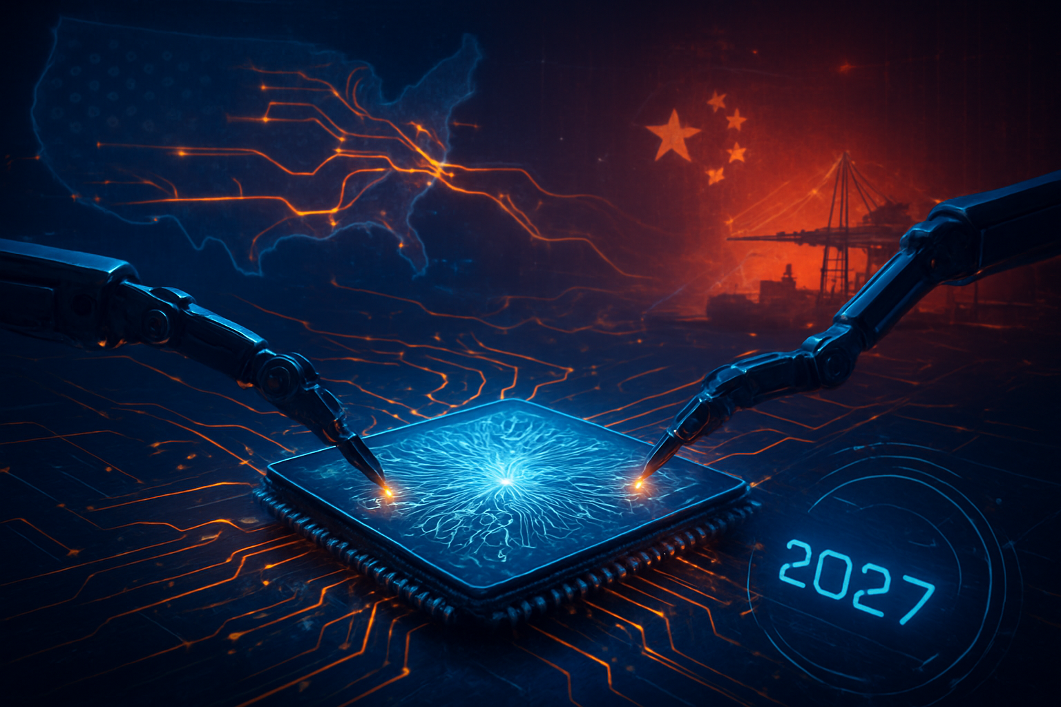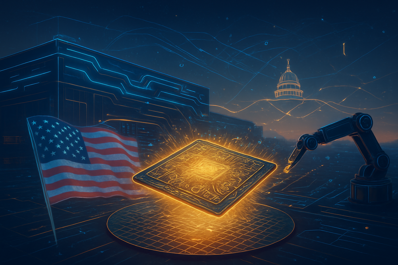
As the artificial intelligence boom pushes the limits of silicon, the semiconductor industry is undergoing its most radical material shift in decades. In a collective move to overcome the "thermal wall" and physical constraints of traditional packaging, industry titans are transitioning from organic (resin-based) substrates to glass core substrates (GCS). This shift, accelerating rapidly as of late 2025, represents a fundamental re-engineering of how the world's most powerful AI processors are built, promising to unlock the trillion-transistor era required for next-generation generative models.
The immediate significance of this transition cannot be overstated. With AI accelerators like NVIDIA’s upcoming architectures demanding power envelopes exceeding 1,000 watts, traditional organic materials—specifically Ajinomoto Build-up Film (ABF)—are reaching their breaking point. Glass offers the structural integrity, thermal stability, and interconnect density that organic materials simply cannot match. By adopting glass, chipmakers are not just improving performance; they are ensuring that the trajectory of AI hardware can keep pace with the exponential growth of AI software.
Breaking the Silicon Ceiling: The Technical Shift to Glass
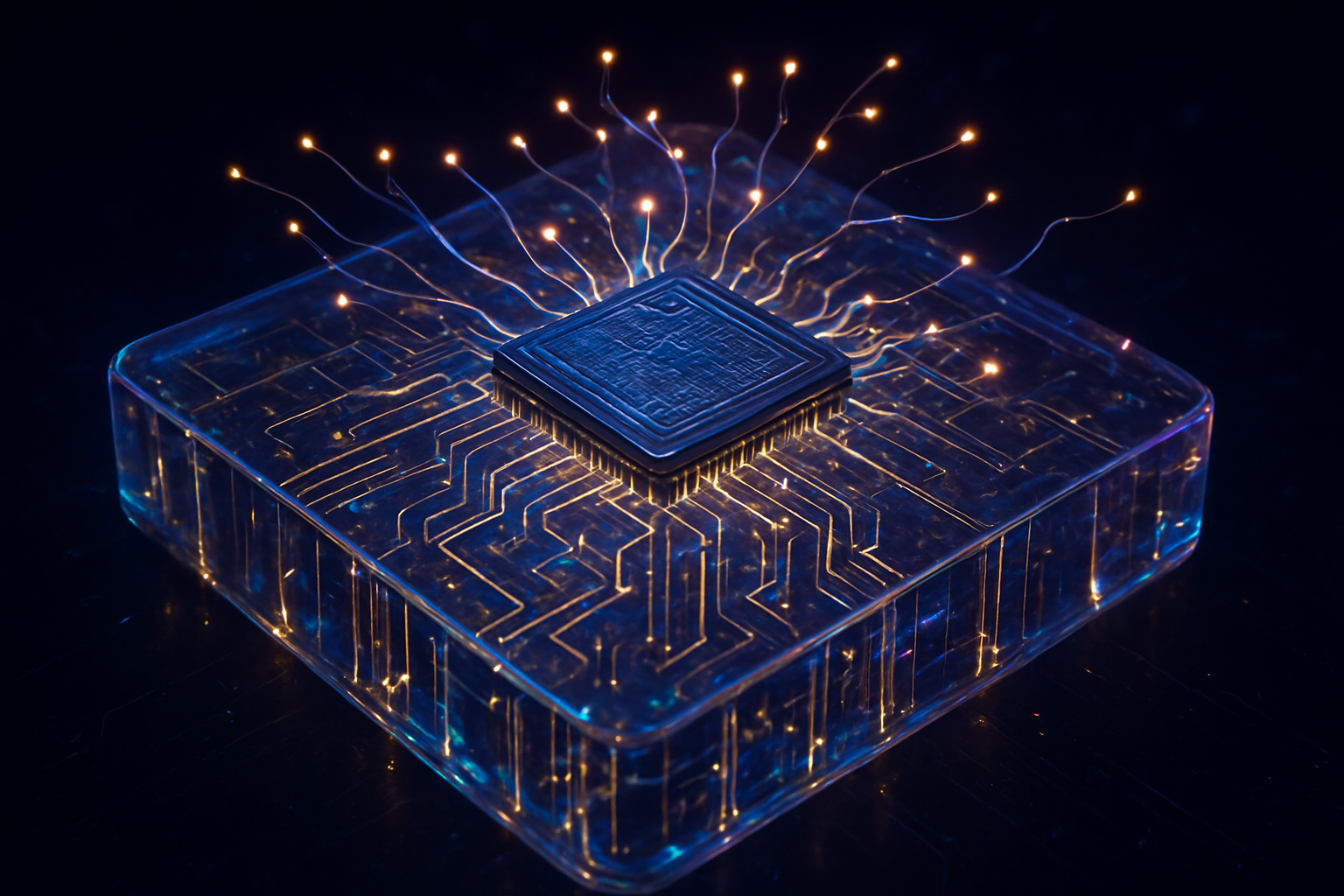
The move toward glass is driven by the physical limitations of current organic substrates, which are prone to warping and heat-induced expansion. Intel (NASDAQ: INTC), a pioneer in this space, has spent over a decade researching glass core technology. In a significant strategic pivot in August 2025, Intel began licensing its GCS intellectual property to external partners, aiming to establish its technology as the industry standard. Glass substrates offer a 10x increase in interconnect density compared to organic materials, allowing for much tighter integration between compute tiles and High-Bandwidth Memory (HBM).
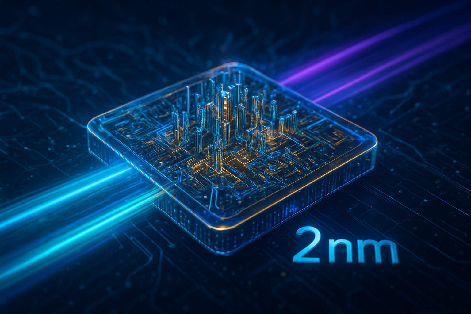
Technically, glass provides several key advantages. Its extreme flatness—often measured at less than 1.0 micrometer—enables precise lithography for sub-2-micron line and space patterning. Furthermore, glass has a Coefficient of Thermal Expansion (CTE) that closely matches silicon. This is critical for AI chips that cycle through extreme temperatures; when the substrate and the silicon die expand and contract at the same rate, the risk of mechanical failure or signal degradation is drastically reduced. Through-Glass Via (TGV) technology, which creates vertical electrical connections through the glass, is the linchpin of this architecture, allowing for high-speed data paths that were previously impossible.
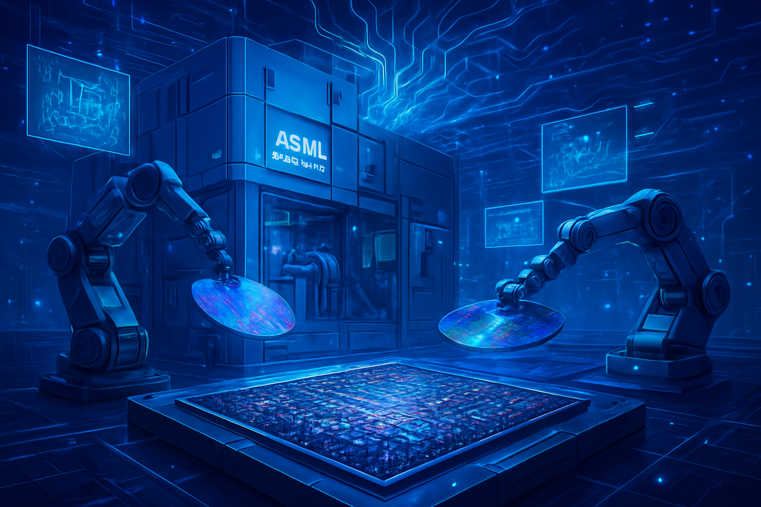
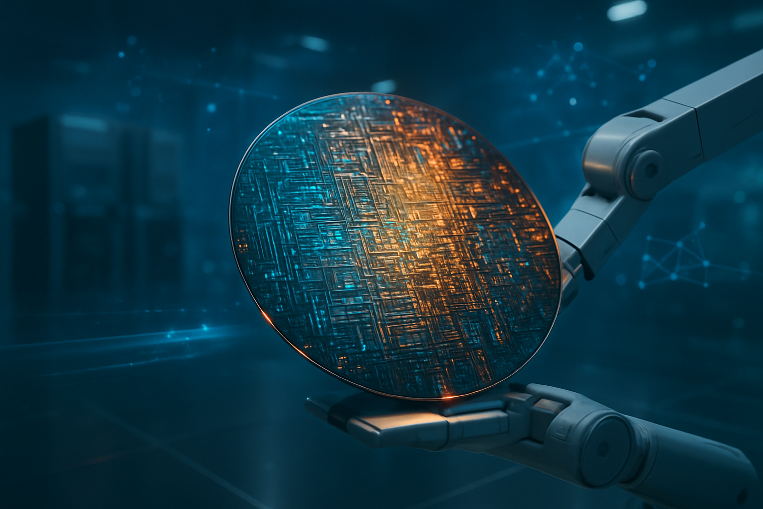
Initial reactions from the research community have been overwhelmingly positive, though tempered by the complexity of the transition. Experts note that while glass is more brittle than organic resin, its ability to support larger "System-in-Package" (SiP) designs is a game-changer. TSMC (NYSE: TSM) has responded to this challenge by aggressively pursuing Fan-Out Panel-Level Packaging (FOPLP) on glass. By using 600mm x 600mm glass panels rather than circular silicon wafers, TSMC can manufacture massive AI accelerators more efficiently, satisfying the relentless demand from customers like NVIDIA (NASDAQ: NVDA).
A New Battleground for AI Dominance
The transition to glass substrates is reshaping the competitive landscape for tech giants and semiconductor foundries alike. Samsung Electronics (KRX: 005930) has mobilized its Samsung Electro-Mechanics division to fast-track a "Glass Core" initiative, launching a pilot line in early 2025. By late 2025, Samsung has reportedly begun supplying GCS samples to major U.S. hyperscalers and chip designers, including AMD (NASDAQ: AMD) and Amazon (NASDAQ: AMZN). This vertical integration strategy positions Samsung as a formidable rival to the Intel-licensed ecosystem and TSMC’s alliance-driven approach.
For AI companies, the benefits are clear. The enhanced thermal management of glass allows for higher clock speeds and more cores without the risk of catastrophic warping. This directly benefits NVIDIA, whose "Rubin" architecture and beyond will rely on these advanced packaging techniques to maintain its lead in the AI training market. Meanwhile, startups focusing on specialized AI silicon may find themselves forced to partner with major foundries early in their design cycles to ensure their chips are compatible with the new glass-based manufacturing pipelines, potentially raising the barrier to entry for high-end hardware.
The disruption extends to the supply chain as well. Companies like Absolics, a subsidiary of SKC (KRX: 011790), have emerged as critical players. Backed by over $100 million in U.S. CHIPS Act grants, Absolics is on track to reach high-volume manufacturing at its Georgia facility by the end of 2025. This localized manufacturing capability provides a strategic advantage for U.S.-based AI labs, reducing reliance on overseas logistics for the most sensitive and advanced components of the AI infrastructure.
The Broader AI Landscape: Overcoming the Thermal Wall
The shift to glass is more than a technical upgrade; it is a necessary evolution to sustain the current AI trajectory. As AI models grow in complexity, the "thermal wall"—the point at which heat dissipation limits performance—has become the primary bottleneck for innovation. Glass substrates represent a breakthrough comparable to the introduction of FinFET transistors or EUV lithography, providing a new foundation for Moore’s Law to continue in the era of heterogeneous integration and chiplets.
Furthermore, glass is the ideal medium for the future of Co-packaged Optics (CPO). As the industry looks toward photonics—using light instead of electricity to move data—the transparency and thermal stability of glass make it the perfect substrate for integrating optical engines directly onto the chip package. This could potentially solve the interconnect bandwidth bottleneck that currently plagues massive AI clusters, allowing for near-instantaneous communication between thousands of GPUs.
However, the transition is not without concerns. The cost of glass substrates remains significantly higher than organic alternatives, and the industry must overcome yield challenges associated with handling brittle glass panels in high-volume environments. Critics argue that the move to glass may further centralize power among the few companies capable of affording the massive R&D and capital expenditures required, potentially slowing innovation in the broader semiconductor ecosystem if standards become fragmented.
The Road Ahead: 2026 and Beyond
Looking toward 2026 and 2027, the semiconductor industry expects to move from the "pre-qualification" phase seen in 2025 to full-scale mass production. Experts predict that the first consumer-facing AI products featuring glass-packaged chips will hit the market by late 2026, likely in high-end data center servers and workstation-class processors. Near-term developments will focus on refining TGV manufacturing processes to drive down costs and improve the robustness of the glass panels during the assembly phase.
In the long term, the applications for glass substrates extend beyond AI. High-performance computing (HPC), 6G telecommunications, and even advanced automotive sensors could benefit from the signal integrity and thermal properties of glass. The challenge will be establishing a unified set of industry standards to ensure interoperability between different vendors' glass cores and chiplets. Organizations like the E-core System Alliance in Taiwan are already working to address these hurdles, but a global consensus remains a work in progress.
A Pivotal Moment in Computing History
The industry-wide pivot to glass substrates marks a definitive end to the era of organic packaging for high-performance computing. By solving the critical issues of thermal expansion and interconnect density, glass provides the structural "scaffolding" necessary for the next decade of AI advancement. This development will likely be remembered as the moment when the physical limitations of materials were finally aligned with the limitless ambitions of artificial intelligence.
In the coming weeks and months, the industry will be watching for the first yield reports from Absolics’ Georgia facility and the results of Samsung’s sample evaluations with U.S. tech giants. As 2025 draws to a close, the "Glass Revolution" is no longer a laboratory curiosity—it is the new standard for the silicon that will power the future of intelligence.
This content is intended for informational purposes only and represents analysis of current AI developments.
TokenRing AI delivers enterprise-grade solutions for multi-agent AI workflow orchestration, AI-powered development tools, and seamless remote collaboration platforms.
For more information, visit https://www.tokenring.ai/.