Tag: AI

  • The Sky is No Longer the Limit: US Air Force Accelerates X-62A VISTA AI Upgrades

    The Sky is No Longer the Limit: US Air Force Accelerates X-62A VISTA AI Upgrades

    The skies over Edwards Air Force Base have long been the testing ground for the future of aviation, but in late 2025, the roar of engines is being matched by the silent, rapid-fire processing of artificial intelligence. The U.S. Air Force’s X-62A Variable Stability In-flight Simulator Test Aircraft (VISTA) has officially entered a transformative new upgrade phase, expanding its mission from basic autonomous maneuvers to complex, multi-agent combat operations. This development marks a pivotal shift in military strategy, moving away from human-centric cockpits toward a future defined by "loyal wingmen" and algorithmic dogfighting.

    As of December 18, 2025, the X-62A has transitioned from proving that AI can fly a fighter jet to proving that AI can lead a fleet. Following a series of historic milestones over the past 24 months—including the first-ever successful autonomous dogfight against a human pilot—the current upgrade program focuses on the "autonomy engine." These enhancements are designed to handle Beyond-Visual-Range (BVR) multi-target engagements and the coordination of multiple autonomous platforms, effectively turning the X-62A into the primary "flying laboratory" for the next generation of American air superiority.

    The Architecture of Autonomy: Inside the X-62A’s "Einstein Box"

    The technical prowess of the X-62A VISTA lies not in its airframe—a modified F-16—but in its unique, open-systems architecture developed by Lockheed Martin (NYSE:LMT). At the core of the aircraft’s recent upgrades is the Enterprise Mission Computer version 2 (EMC2), colloquially known as the "Einstein Box." This high-performance processor acts as the brain of the operation, running sophisticated machine learning agents while remaining physically and logically isolated from the aircraft's primary flight control laws. This separation is a critical safety feature, ensuring that even if an AI agent makes an unpredictable decision, the underlying flight system can override it to maintain structural integrity.

    The integration of these AI agents is facilitated by the System for Autonomous Control of the Simulation (SACS), a layer developed by Calspan, a subsidiary of TransDigm Group Inc. (NYSE:TDG). SACS provides a "safety sandbox" that allows non-deterministic, self-learning algorithms to operate in a real-world environment without risking the loss of the aircraft. Complementing this is Lockheed Martin’s Model Following Algorithm (MFA), which allows the X-62A to mimic the flight characteristics of other aircraft. This means the VISTA can effectively "pretend" to be a next-generation drone or a stealth fighter, allowing the AI to learn how to handle different aerodynamic profiles in real-time.

    What sets the X-62A apart from previous autonomous efforts is its reliance on reinforcement learning (RL). Unlike traditional "if-then" programming, RL allows the AI to develop its own tactics through millions of simulated trials. During the DARPA Air Combat Evolution (ACE) program tests, this resulted in AI pilots that were more aggressive and precise than their human counterparts, maintaining tactical advantages in high-G maneuvers that would push a human pilot to their physical limits. The late 2025 upgrades further enhance this by increasing the onboard computing power, allowing for more complex "multi-agent" scenarios where the X-62A must coordinate with other autonomous jets to overwhelm an adversary.

    A Competitive Shift: Defense Tech Giants and AI Startups

    The success of the VISTA program is reshaping the competitive landscape of the defense industry. While legacy contractors like Lockheed Martin (NYSE:LMT) continue to provide the hardware and foundational architecture, the "software-defined" nature of modern warfare has opened the door for specialized AI firms. Companies like Shield AI, which provides the Hivemind autonomy engine, have become central to the Air Force’s strategy. Shield AI’s ability to iterate on flight software in weeks rather than years represents a fundamental disruption to the traditional defense procurement cycle.

    Other players, such as EpiSci and PhysicsAI, are also benefiting from the X-62A’s open-architecture approach. By creating an "algorithmic league" where different companies can upload their AI agents to the VISTA for head-to-head testing, the Air Force has fostered a competitive ecosystem that rewards performance over pedigree. This shift is forcing major aerospace firms to pivot toward software-centric models, as the value of a platform is increasingly determined by the intelligence of its autonomy engine rather than the speed of its airframe.

    Market analysts suggest that the X-62A program is a harbinger of massive spending shifts in the Pentagon’s budget. The move toward the Collaborative Combat Aircraft (CCA) program—which aims to build thousands of low-cost, autonomous "loyal wingmen"—is expected to divert billions from traditional manned fighter programs. For tech giants and AI startups alike, the X-62A serves as the ultimate validation of their technology, proving that AI can handle the most "non-deterministic" and high-stakes environment imaginable: the cockpit of a fighter jet.

    The Global Implications of Algorithmic Warfare

    The broader significance of the X-62A VISTA upgrades cannot be overstated. We are witnessing the dawn of the "Third Posture" in military aviation, where mass and machine learning replace the reliance on a small number of highly expensive, manned platforms. This transition mirrors the move from propeller planes to jets, or from visual-range combat to radar-guided missiles. By proving that AI can safely and effectively navigate the complexities of aerial combat, the U.S. Air Force is signaling a future where human pilots act more as "mission commanders," overseeing a swarm of autonomous agents from a safe distance.

    However, this advancement brings significant ethical and strategic concerns. The use of "non-deterministic" AI—systems that can learn and change their behavior—in lethal environments raises questions about accountability and the potential for unintended escalation. The Air Force has addressed these concerns by emphasizing that a human is always "on the loop" for lethal decisions, but the sheer speed of AI-driven combat may eventually make human intervention a bottleneck. Furthermore, the X-62A’s success has accelerated a global AI arms race, with peer competitors like China and Russia reportedly fast-tracking their own autonomous flight programs to keep pace with American breakthroughs.

    Comparatively, the X-62A milestones of 2024 and 2025 are being viewed by historians as the "Kitty Hawk moment" for autonomous systems. Just as the first flight changed the nature of geography and warfare, the first AI dogfight at Edwards AFB has changed the nature of tactical decision-making. The ability to process vast amounts of sensor data and execute maneuvers in milliseconds gives autonomous systems a "cognitive advantage" that will likely define the outcome of future conflicts.

    The Horizon: From VISTA to Project VENOM

    Looking ahead, the data gathered from the X-62A VISTA is already being funneled into Project VENOM (Viper Experimentation and Next-gen Operations Model). While the X-62A remains a single, highly specialized testbed, Project VENOM has seen the conversion of six standard F-16s into autonomous testbeds at Eglin Air Force Base. This move toward a larger fleet of autonomous Vipers indicates that the Air Force is ready to scale its AI capabilities from experimental labs to operational squadrons.

    The ultimate goal is the full deployment of the Collaborative Combat Aircraft (CCA) program by the late 2020s. Experts predict that the lessons learned from the late 2025 X-62A upgrades—specifically regarding multi-agent coordination and BVR combat—will be the foundation for the CCA's initial operating capability. Challenges remain, particularly in the realm of secure data links and the "trust" between human pilots and their AI wingmen, but the trajectory is clear. The next decade of military aviation will be defined by the seamless integration of human intuition and machine precision.

    A New Chapter in Aviation History

    The X-62A VISTA upgrade program is more than just a technical refinement; it is a declaration of intent. By successfully moving from 1-on-1 dogfighting to complex multi-agent simulations, the U.S. Air Force has proven that artificial intelligence is no longer a peripheral tool, but the central nervous system of modern air power. The milestones achieved at Edwards Air Force Base over the last two years have dismantled the long-held belief that the "human touch" was irreplaceable in the cockpit.

    As we move into 2026, the industry should watch for the first results of the multi-agent BVR tests and the continued expansion of Project VENOM. The X-62A has fulfilled its role as the pioneer, carving a path through the unknown and establishing the safety and performance standards that will govern the autonomous fleets of tomorrow. The sky is no longer a limit for AI; it is its new home.


    This content is intended for informational purposes only and represents analysis of current AI developments.

    TokenRing AI delivers enterprise-grade solutions for multi-agent AI workflow orchestration, AI-powered development tools, and seamless remote collaboration platforms.
    For more information, visit https://www.tokenring.ai/.

  • The Silicon Green Rush: How Texas and Gujarat are Powering the AI Revolution with Clean Energy

    The Silicon Green Rush: How Texas and Gujarat are Powering the AI Revolution with Clean Energy

    As the global demand for artificial intelligence reaches a fever pitch, the semiconductor industry is facing an existential reckoning: how to produce the world’s most advanced chips without exhausting the planet’s resources. In a landmark shift for 2025, the industry’s two most critical growth hubs—Texas and Gujarat, India—have become the front lines for a new era of "Green Fabs." These multi-billion dollar manufacturing sites are no longer just about transistor density; they are being engineered as self-sustaining ecosystems powered by massive solar and wind arrays to mitigate the staggering environmental costs of AI hardware production.

    The immediate significance of this transition cannot be overstated. With the International Energy Agency (IEA) warning that data center electricity consumption could double to nearly 1,000 TWh by 2030, the "embodied carbon" of the chips themselves has become a primary concern for tech giants. By integrating renewable energy directly into the fabrication process, companies like Samsung Electronics (KRX: 005930), Texas Instruments (NASDAQ: TXN), and the Tata Group are attempting to decouple the explosive growth of AI from its carbon footprint, effectively rebranding silicon as a "low-carbon" commodity.

    Technical Foundations: The Rise of the Sustainable Mega-Fab

    The technical complexity of a modern semiconductor fab is unparalleled, requiring millions of gallons of ultrapure water (UPW) and gigawatts of electricity to operate. In Texas, Samsung’s Taylor facility—a $40 billion investment—is setting a new benchmark for resource efficiency. The site, which began installing equipment for 2nm chip production in late 2024, utilizes a "closed-loop" water system designed to reclaim and reuse up to 75% of process water. This is a critical advancement over legacy fabs, which often discharged millions of gallons of wastewater daily. Furthermore, Samsung has leveraged its participation in the RE100 initiative to secure 100% renewable electricity for its U.S. operations through massive Power Purchase Agreements (PPAs) with Texas wind and solar providers.

    Across the globe in Gujarat, India, Tata Electronics has broken ground on the country’s first "Mega Fab" in the Dholera Special Investment Region. This facility is uniquely positioned within one of the world’s largest renewable energy zones, drawing power from the Dholera Solar Park. In partnership with Powerchip Semiconductor Manufacturing Corp (PSMC), Tata is implementing "modularization" in its construction to reduce the carbon footprint of the build-out phase. The technical goal is to achieve near-zero liquid discharge (ZLD) from day one, a necessity in the water-scarce climate of Western India. These "greenfield" projects differ from older "brownfield" upgrades because sustainability is baked into the architectural DNA of the plant, utilizing AI-driven "digital twin" models to optimize energy flow in real-time.

    Initial reactions from the industry have been overwhelmingly positive, though tempered by the scale of the challenge. Analysts at TechInsights noted in late 2025 that the shift to High-NA EUV (Extreme Ultraviolet) lithography—while energy-intensive—is actually a "green" win. These machines, produced by ASML (NASDAQ: ASML), allow for single-exposure patterning that eliminates dozens of chemical-heavy processing steps, effectively reducing the energy used per wafer by an estimated 200 kWh.

    Strategic Positioning: Sustainability as a Competitive Moat

    The move toward green manufacturing is not merely an altruistic endeavor; it is a calculated strategic play. As major AI players like Nvidia (NASDAQ: NVDA), Apple (NASDAQ: AAPL), and Tesla (NASDAQ: TSLA) face tightening ESG (Environmental, Social, and Governance) reporting requirements, such as the EU’s Corporate Sustainability Reporting Directive (CSRD), they are increasingly favoring suppliers who can provide "low-carbon silicon." For these companies, the carbon footprint of their supply chain (Scope 3 emissions) is the hardest to control, making a green fab in Texas or Gujarat a highly attractive partner.

    Texas Instruments has already capitalized on this trend. As of December 17, 2025, TI announced that its 300mm manufacturing operations are now 100% powered by renewable energy. By providing clients with precise carbon-intensity data per chip, TI has created "transparency as a service," allowing Apple to calculate the exact footprint of the power management chips used in the latest iPhones. This level of data granularity has become a significant competitive advantage, potentially disrupting older fabs that cannot provide such detailed environmental metrics.

    In India, Tata Electronics is positioning itself as a "georesilient" and sustainable alternative to East Asian manufacturing hubs. By offering 100% green-powered production, Tata is courting Western firms looking to diversify their supply chains while maintaining their net-zero commitments. This market positioning is particularly relevant for the AI sector, where the "energy crisis" of training large language models (LLMs) has put a spotlight on the environmental ethics of the entire hardware stack.

    The Wider Significance: Mitigating the AI Energy Crisis

    The integration of clean energy into fab projects fits into a broader global trend of "Green AI." For years, the focus was solely on making AI models more efficient (algorithmic efficiency). However, the industry has realized that the hardware itself is the bottleneck. The environmental challenges are daunting: a single modern fab can consume as much water as a small city. In Gujarat, the government has had to commission a dedicated desalination plant for the Dholera region to ensure that the semiconductor industry doesn't compete with local agriculture for water.

    There are also potential concerns regarding "greenwashing" and the reliability of renewable grids. Solar and wind are intermittent, while a semiconductor fab requires 24/7 "five-nines" reliability—99.999% uptime. To address this, 2025 has seen a surge in interest in Small Modular Reactors (SMRs) and advanced battery storage to provide carbon-free baseload power. This marks a significant departure from previous industry milestones; while the 2010s were defined by the "mobile revolution" and a focus on battery life, the 2020s are being defined by the "AI revolution" and a focus on planetary sustainability.

    The ethical implications are also coming to the fore. As fabs move into regions like Texas and Gujarat, they bring high-paying jobs but also place immense pressure on local utilities. The "Texas Miracle" of low-cost energy is being tested by the sheer volume of new industrial demand, leading to a complex dialogue between tech giants, local communities, and environmental advocates regarding who gets priority during grid-stress events.

    Future Horizons: From Solar Parks to Nuclear Fabs

    Looking ahead to 2026 and beyond, the industry is expected to move toward even more radical energy solutions. Experts predict that the next generation of fabs will likely feature on-site nuclear micro-reactors to ensure a steady stream of carbon-free energy. Microsoft (NASDAQ: MSFT) and Intel (NASDAQ: INTC) have already begun exploring such partnerships, signaling that the "solar/wind" era may be just the first step in a longer journey toward energy independence for the semiconductor sector.

    Another frontier is the development of "circular silicon." Companies are researching ways to reclaim rare earth metals and high-purity chemicals from decommissioned chips and manufacturing waste. If successful, this would transition the industry from a linear "take-make-waste" model to a circular economy, further reducing the environmental impact of the AI revolution. The challenge remains the extreme purity required for chipmaking; any recycled material must meet the same "nine-nines" (99.9999999%) purity standards as virgin material.

    Conclusion: A New Standard for the AI Era

    The transition to clean-energy-powered fabs in Gujarat and Texas represents a watershed moment in the history of technology. It is a recognition that the "intelligence" provided by AI cannot come at the cost of the environment. The key takeaways from 2025 are clear: sustainability is now a core technical specification, water recycling is a prerequisite for expansion, and "low-carbon silicon" is the new gold standard for the global supply chain.

    As we look toward 2026, the industry’s success will be measured not just by Moore’s Law, but by its ability to scale responsibly. The "Green AI" movement has successfully moved from the fringe to the center of corporate strategy, and the massive projects in Texas and Gujarat are the physical manifestations of this shift. For investors, policymakers, and consumers, the message is clear: the future of AI is being written in silicon, but it is being powered by the sun and the wind.


    This content is intended for informational purposes only and represents analysis of current AI developments.

    TokenRing AI delivers enterprise-grade solutions for multi-agent AI workflow orchestration, AI-powered development tools, and seamless remote collaboration platforms.
    For more information, visit https://www.tokenring.ai/.

  • The Trillion-Dollar Nexus: OpenAI’s Funding Surge and the Race for Global AI Sovereignty

    The Trillion-Dollar Nexus: OpenAI’s Funding Surge and the Race for Global AI Sovereignty

    SAN FRANCISCO — December 18, 2025 — OpenAI is currently navigating a transformative period that is reshaping the global technology landscape, as the company enters the final stages of a historic $100 billion funding round. This massive capital injection, which values the AI pioneer at a staggering $750 billion, is not merely a play for software dominance but the cornerstone of a radical shift toward vertical integration. By securing unprecedented levels of investment from entities like SoftBank Group Corp. (OTC:SFTBY), Thrive Capital, and a strategic $10 billion-plus commitment from Amazon.com, Inc. (NASDAQ:AMZN), OpenAI is positioning itself to bridge the "electron gap" and the chronic shortage of high-performance semiconductors that have defined the AI era.

    The immediate significance of this development lies in the decoupling of OpenAI from its total reliance on merchant silicon. While the company remains a primary customer of NVIDIA Corporation (NASDAQ:NVDA), this new funding is being funneled into "Stargate LLC," a multi-national joint venture designed to build "gigawatt-scale" data centers and proprietary AI chips. This move signals the end of the "software-only" era for AI labs, as Sam Altman’s vision for AI infrastructure begins to dictate the roadmap for the entire semiconductor industry, forcing a realignment of global supply chains and energy policies.

    The Architecture of "Stargate": Custom Silicon and Gigawatt-Scale Compute

    At the heart of OpenAI’s infrastructure push is a custom Application-Specific Integrated Circuit (ASIC) co-developed with Broadcom Inc. (NASDAQ:AVGO). Unlike the general-purpose power of NVIDIA’s upcoming Rubin architecture, the OpenAI-Broadcom chip is a "bespoke" inference engine built on Taiwan Semiconductor Manufacturing Company’s (NYSE:TSM) 3nm process. Technical specifications reveal a systolic array design optimized for the dense matrix multiplications inherent in Transformer-based models like the recently teased "o2" reasoning engine. By stripping away the flexibility required for non-AI workloads, OpenAI aims to reduce the power consumption per token by an estimated 30% compared to off-the-shelf hardware.

    The physical manifestation of this vision is "Project Ludicrous," a 1.2-gigawatt data center currently under construction in Abilene, Texas. This site is the first of many planned under the Stargate LLC umbrella, a partnership that now includes Oracle Corporation (NYSE:ORCL) and the Abu Dhabi-backed MGX. These facilities are being designed with liquid-cooling at their core to handle the 1,800W thermal design power (TDP) of modern AI racks. Initial reactions from the research community have been a mix of awe and concern; while the scale promises a leap toward Artificial General Intelligence (AGI), experts warn that the sheer concentration of compute power in a single entity’s hands creates a "compute moat" that may be insurmountable for smaller rivals.

    A New Semiconductor Order: Winners, Losers, and Strategic Pivots

    The ripple effects of OpenAI’s funding and infrastructure plans are being felt across the "Magnificent Seven" and the broader semiconductor market. Broadcom has emerged as a primary beneficiary, now controlling nearly 89% of the custom AI ASIC market as it helps OpenAI, Meta Platforms, Inc. (NASDAQ:META), and Alphabet Inc. (NASDAQ:GOOGL) design their own silicon. Meanwhile, NVIDIA has responded to the threat of custom chips by accelerating its product cycle to a yearly cadence, moving from Blackwell to the Rubin (R100) platform in record time to maintain its performance lead in training-heavy workloads.

    For tech giants like Amazon and Microsoft Corporation (NASDAQ:MSFT), the relationship with OpenAI has become increasingly complex. Amazon’s $10 billion investment is reportedly tied to OpenAI’s adoption of Amazon’s Trainium chips, a strategic move by the e-commerce giant to ensure its own silicon finds a home in the world’s most advanced AI models. Conversely, Microsoft, while still a primary partner, is seeing OpenAI diversify its infrastructure through Stargate LLC to avoid vendor lock-in. This "multi-vendor" strategy has also provided a lifeline to Advanced Micro Devices, Inc. (NASDAQ:AMD), whose MI300X and MI350 series chips are being used as critical bridging hardware until OpenAI’s custom silicon reaches mass production in late 2026.

    The Electron Gap and the Geopolitics of Intelligence

    Beyond the chips themselves, Sam Altman’s vision has highlighted a looming crisis in the AI landscape: the "electron gap." As OpenAI aims for 100 GW of new energy capacity per year to fuel its scaling laws, the company has successfully lobbied the U.S. government to treat AI infrastructure as a national security priority. This has led to a resurgence in nuclear energy investment, with startups like Oklo Inc. (NYSE:OKLO)—where Altman serves as chairman—breaking ground on fission sites to power the next generation of data centers. The transition to a Public Benefit Corporation (PBC) in October 2025 was a key prerequisite for this, allowing OpenAI to raise the trillions needed for energy and foundries without the constraints of a traditional profit cap.

    This massive scaling effort is being compared to the Manhattan Project or the Apollo program in its scope and national significance. However, it also raises profound environmental and social concerns. The 10 GW of power OpenAI plans to consume by 2029 is equivalent to the energy usage of several small nations, leading to intense scrutiny over the carbon footprint of "reasoning" models. Furthermore, the push for "Sovereign AI" has sparked a global arms race, with the UK, UAE, and Australia signing deals for their own Stargate-class data centers to ensure they are not left behind in the transition to an AI-driven economy.

    The Road to 2026: What Lies Ahead for AI Infrastructure

    Looking toward 2026, the industry expects the first "silicon-validated" results from the OpenAI-Broadcom partnership. If these custom chips deliver the promised efficiency gains, it could lead to a permanent shift in how AI is monetized, significantly lowering the "cost-per-query" and enabling widespread integration of high-reasoning agents in consumer devices. However, the path is fraught with challenges, most notably the advanced packaging bottleneck at TSMC. The global supply of CoWoS (Chip-on-Wafer-on-Substrate) remains the single greatest constraint on OpenAI’s ambitions, and any geopolitical instability in the Taiwan Strait could derail the entire $1.4 trillion infrastructure plan.

    In the near term, the AI community is watching for the official launch of GPT-5, which is expected to be the first model trained on a cluster of over 100,000 H100/B200 equivalents. Analysts predict that the success of this model will determine whether the massive capital expenditures of 2025 were a visionary investment or a historic overreach. As OpenAI prepares for a potential IPO in late 2026, the focus will shift from "how many chips can they buy" to "how efficiently can they run the chips they have."

    Conclusion: The Dawn of the Infrastructure Era

    The ongoing funding talks and infrastructure maneuvers of late 2025 mark a definitive turning point in the history of artificial intelligence. OpenAI is no longer just an AI lab; it is becoming a foundational utility company for the cognitive age. By integrating chip design, energy production, and model development, Sam Altman is attempting to build a vertically integrated empire that rivals the industrial titans of the 20th century. The significance of this development cannot be overstated—it represents a bet that the future of the global economy will be written in silicon and powered by nuclear-backed data centers.

    As we move into 2026, the key metrics to watch will be the progress of "Project Ludicrous" in Texas and the stability of the burgeoning partnership between OpenAI and the semiconductor giants. Whether this trillion-dollar gamble leads to the realization of AGI or serves as a cautionary tale of "compute-maximalism," one thing is certain: the relationship between AI funding and hardware demand has fundamentally altered the trajectory of the tech industry.


    This content is intended for informational purposes only and represents analysis of current AI developments.

    TokenRing AI delivers enterprise-grade solutions for multi-agent AI workflow orchestration, AI-powered development tools, and seamless remote collaboration platforms.
    For more information, visit https://www.tokenring.ai/.
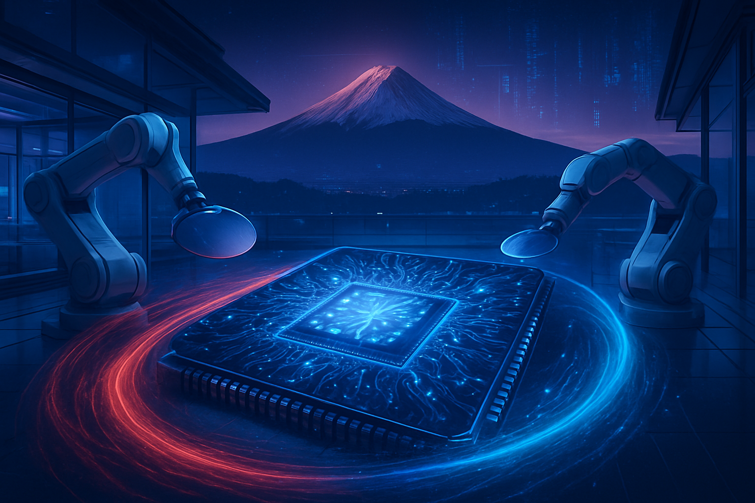
  • The Great Silicon Deconstruction: How Chiplets Are Breaking the Physical Limits of AI

    The Great Silicon Deconstruction: How Chiplets Are Breaking the Physical Limits of AI

    The semiconductor industry has reached a historic inflection point in late 2025, marking the definitive end of the "Big Iron" era of monolithic chip design. For decades, the goal of silicon engineering was to cram as many transistors as possible onto a single, continuous slab of silicon. However, as artificial intelligence models have scaled into the tens of trillions of parameters, the physical and economic limits of this "monolithic" approach have finally shattered. In its place, a modular revolution has taken hold: the shift to chiplet architectures.

    This transition represents a fundamental reimagining of how computers are built. Rather than a single massive processor, modern AI accelerators like the NVIDIA (NASDAQ: NVDA) Rubin and AMD (NASDAQ: AMD) Instinct MI400 are now constructed like high-tech LEGO sets. By breaking a processor into smaller, specialized "chiplets"—some for intense mathematical calculation, others for memory management or high-speed data transfer—manufacturers are overcoming the "reticle limit," the physical boundary of how large a single chip can be printed. This modularity is not just a technical curiosity; it is the primary engine allowing AI performance to continue doubling even as traditional Moore’s Law scaling slows to a crawl.

    Breaking the Reticle Limit: The Physics of Modular Silicon

    The technical catalyst for the chiplet shift is the "reticle limit," a physical constraint of lithography machines that prevents them from printing a single chip larger than approximately 858mm². As of late 2025, the demand for AI compute has far outstripped what can fit within that tiny square. To solve this, manufacturers are using advanced packaging techniques like TSMC (NYSE: TSM) CoWoS-L (Chip-on-Wafer-on-Substrate with Local Silicon Interconnect) to "stitch" multiple dies together. The recently unveiled NVIDIA Rubin architecture, for instance, effectively creates a "4x reticle" footprint, enabling a level of compute density that would be physically impossible to manufacture as a single piece of silicon.

    Beyond sheer size, the move to chiplets has solved the industry’s most pressing economic headache: yield rates. In a monolithic 3nm design, a single microscopic defect can ruin an entire $10,000 chip. By disaggregating the design into smaller chiplets, manufacturers can test each module individually as a "Known Good Die" (KGD) before assembly. This has pushed effective manufacturing yields for top-tier AI accelerators from the 50-60% range seen in 2023 to over 85% today. If one small chiplet is defective, only that tiny piece is discarded, drastically reducing waste and stabilizing the astronomical costs of leading-edge semiconductor fabrication.

    Furthermore, chiplets enable "heterogeneous integration," allowing engineers to mix and match different manufacturing processes within the same package. In a 2025-era AI processor, the core "brain" might be built on an expensive, ultra-efficient 2nm or 3nm node, while the less-sensitive I/O and memory controllers remain on more mature, cost-effective 5nm or 7nm nodes. This "node optimization" ensures that every dollar of capital expenditure is directed toward the components that provide the greatest performance benefit, preventing a total collapse of the price-to-performance ratio in the AI sector.

    Initial reactions from the AI research community have been overwhelmingly positive, particularly regarding the integration of HBM4 (High Bandwidth Memory). By stacking memory chiplets directly on top of or adjacent to the compute dies, manufacturers are finally bridging the "memory wall"—the bottleneck where processors sit idle while waiting for data. Experts at the 2025 IEEE International Solid-State Circuits Conference noted that this modular approach has enabled a 400% increase in memory bandwidth over the last two years, a feat that would have been unthinkable under the old monolithic paradigm.

    Strategic Realignment: Hyperscalers and the Custom Silicon Moat

    The chiplet revolution has fundamentally altered the competitive landscape for tech giants and AI labs. No longer content to be mere customers of the major chipmakers, hyperscalers like Amazon (NASDAQ: AMZN), Alphabet (NASDAQ: GOOGL), and Meta (NASDAQ: META) have become architects of their own modular silicon. Amazon’s recently launched Trainium3, for example, utilizes a dual-chiplet design that allows AWS to offer AI training credits at nearly 60% lower costs than traditional GPU instances. By using chiplets to lower the barrier to entry for custom hardware, these companies are building a "silicon moat" that optimizes their specific internal workloads, such as recommendation engines or large language model (LLM) inference.

    For established chipmakers, the transition has sparked a fierce strategic battle over packaging dominance. While NVIDIA (NASDAQ: NVDA) remains the performance king with its Rubin and Blackwell platforms, Intel (NASDAQ: INTC) has leveraged its Foveros 3D packaging technology to secure massive foundry wins, including Microsoft (NASDAQ: MSFT) and its Maia 200 series. Intel’s ability to offer "Secure Enclave" manufacturing within the United States has become a significant strategic advantage as geopolitical tensions continue to cloud the future of the global supply chain. Meanwhile, Samsung (KRX: 005930) has positioned itself as a "one-stop shop," integrating its own HBM4 memory with proprietary 2.5D packaging to offer a vertically integrated alternative to the TSMC-NVIDIA duopoly.

    The disruption extends to the startup ecosystem as well. The maturation of the UCIe 3.0 (Universal Chiplet Interconnect Express) standard has created a "Chiplet Economy," where smaller hardware startups like Tenstorrent and Etched can buy "off-the-shelf" I/O and memory chiplets. This allows them to focus their limited R&D budgets on designing a single, high-value AI logic chiplet rather than an entire complex SoC. This democratization of hardware design has reduced the capital required for a first-generation tape-out by an estimated 40%, leading to a surge in specialized AI hardware tailored for niche applications like edge robotics and medical diagnostics.

    The Wider Significance: A New Era for Moore’s Law

    The shift to chiplets is more than a manufacturing tweak; it is the birth of "Moore’s Law 2.0." While the physical shrinking of transistors is reaching its atomic limit, the ability to scale systems through modularity provides a new path forward for the AI landscape. This trend fits into the broader move toward "system-level" scaling, where the unit of compute is no longer a single chip or even a single server, but the entire data center rack. As we move through the end of 2025, the industry is increasingly viewing the data center as one giant, disaggregated computer, with chiplets serving as the interchangeable components of its massive brain.

    However, this transition is not without concerns. The complexity of testing and assembling multi-die packages is immense, and the industry’s heavy reliance on TSMC (NYSE: TSM) for advanced packaging remains a significant single point of failure. Furthermore, as chips become more modular, the power density within a single package has skyrocketed, leading to unprecedented thermal management challenges. The shift toward liquid cooling and even co-packaged optics is no longer a luxury but a requirement for the next generation of AI infrastructure.

    Comparatively, the chiplet milestone is being viewed by industry historians as significant as the transition from vacuum tubes to transistors, or the move from single-core to multi-core CPUs. It represents a shift from a "fixed" hardware mindset to a "fluid" one, where hardware can be as iterative and modular as the software it runs. This flexibility is crucial in a world where AI models are evolving faster than the 18-to-24-month design cycle of traditional semiconductors.

    The Horizon: Glass Substrates and Optical Interconnects

    Looking toward 2026 and beyond, the industry is already preparing for the next phase of the chiplet evolution. One of the most anticipated near-term developments is the commercialization of glass core substrates. Led by research from Intel (NASDAQ: INTC) and TSMC (NYSE: TSM), glass offers superior flatness and thermal stability compared to the organic materials used today. This will allow for even larger package sizes, potentially accommodating up to 12 or 16 HBM4 stacks on a single interposer, further pushing the boundaries of memory capacity for the next generation of "Super-LLMs."

    Another frontier is the integration of Co-Packaged Optics (CPO). As data moves between chiplets, traditional electrical signals generate significant heat and consume a large portion of the chip’s power budget. Experts predict that by late 2026, we will see the first widespread use of optical chiplets that use light rather than electricity to move data between dies. This would effectively eliminate the "communication wall," allowing for near-instantaneous data transfer across a rack of thousands of chips, turning a massive cluster into a single, unified compute engine.

    The challenges ahead are primarily centered on standardization and software. While UCIe has made great strides, ensuring that a chiplet from one vendor can talk seamlessly to a chiplet from another remains a hurdle. Additionally, compilers and software stacks must become "chiplet-aware" to efficiently distribute workloads across these fragmented architectures. Nevertheless, the trajectory is clear: the future of AI is modular.

    Conclusion: The Modular Future of Intelligence

    The shift from monolithic to chiplet architectures marks the most significant architectural change in the semiconductor industry in decades. By overcoming the physical limits of lithography and the economic barriers of declining yields, chiplets have provided the runway necessary for the AI revolution to continue its exponential growth. The success of platforms like NVIDIA’s Rubin and AMD’s MI400 has proven that the "LEGO-like" approach to silicon is not just viable, but essential for the next decade of compute.

    As we look toward 2026, the key takeaways are clear: packaging is the new Moore’s Law, custom silicon is the new strategic moat for hyperscalers, and the "deconstruction" of the data center is well underway. The industry has moved from asking "how small can we make a chip?" to "how many pieces can we connect?" This change in perspective ensures that while the physical limits of silicon may be in sight, the limits of artificial intelligence remain as distant as ever. In the coming months, watch for the first high-volume deployments of HBM4 and the initial pilot programs for glass substrates—these will be the bellwethers for the next stage of the modular era.


    This content is intended for informational purposes only and represents analysis of current AI developments.

    TokenRing AI delivers enterprise-grade solutions for multi-agent AI workflow orchestration, AI-powered development tools, and seamless remote collaboration platforms.
    For more information, visit https://www.tokenring.ai/.

  • The Trillion-Dollar Gamble: Wall Street Braces for the AI Infrastructure “Financing Bubble”

    The Trillion-Dollar Gamble: Wall Street Braces for the AI Infrastructure “Financing Bubble”

    The artificial intelligence revolution has reached a precarious crossroads where the digital world meets the physical limits of the global economy. The "Big Four" hyperscalers—Microsoft Corp. (NASDAQ: MSFT), Alphabet Inc. (NASDAQ: GOOGL), Amazon.com Inc. (NASDAQ: AMZN), and Meta Platforms Inc. (NASDAQ: META)—have collectively pushed their annual capital expenditure (CAPEX) toward a staggering $400 billion. This unprecedented spending spree, aimed at erecting gigawatt-scale data centers and securing massive stockpiles of high-end chips, has ignited a fierce debate on Wall Street. While proponents argue this is the necessary foundation for a new industrial era, a growing chorus of analysts warns of a "financing bubble" fueled by circular revenue models and over-leveraged infrastructure debt.

    The immediate significance of this development lies in the shifting nature of tech investment. We are no longer in the era of "lean software" startups; we have entered the age of "heavy silicon" and "industrial AI." The sheer scale of the required capital has forced tech giants to seek unconventional financing, bringing private equity titans like Blackstone Inc. (NYSE: BX) and Brookfield Asset Management (NYSE: BAM) into the fold as the "new utilities" of the digital age. However, as 2025 draws to a close, the first cracks in this massive financial edifice are beginning to appear, with high-profile project cancellations and power grid failures signaling that the "Great Execution" phase of AI may be more difficult—and more expensive—than anyone anticipated.

    The Architecture of the AI Arms Race

    The technical and financial architecture supporting the AI build-out in 2025 differs radically from previous cloud expansions. Unlike the general-purpose data centers of the 2010s, today’s "AI Gigafactories" are purpose-built for massive-scale training and inference, requiring specialized power cooling and liquid-cooled racks to support clusters of hundreds of thousands of GPUs. To fund these behemoths, a new tier of "neocloud" providers like CoreWeave and Lambda Labs has pioneered the use of GPU-backed debt. In this model, the latest H100 and B200 chips from NVIDIA Corp. (NASDAQ: NVDA) serve as collateral for multi-billion dollar loans. As of late 2025, over $20 billion in such debt has been issued, often structured through Special Purpose Vehicles (SPVs) that allow companies to keep massive infrastructure liabilities off their primary corporate balance sheets.

    This shift toward asset-backed financing has been met with mixed reactions from the AI research community and industry experts. While researchers celebrate the unprecedented compute power now available for "Agentic AI" and frontier models, financial experts are drawing uncomfortable parallels to the "vendor-financing" bubble of the 1990s fiber-optic boom. In that era, equipment manufacturers financed their own customers to inflate sales figures—a dynamic some see mirrored today as hyperscalers invest in AI startups like OpenAI and Anthropic, who then use those very funds to purchase cloud credits from their investors. This "circularity" has raised concerns that the current revenue growth in the AI sector may be an accounting mirage rather than a reflection of genuine market demand.

    The technical specifications of these projects are also hitting a physical wall. The North American Electric Reliability Corporation (NERC) recently issued a winter reliability alert for late 2025, noting that AI-driven demand has added 20 gigawatts to the U.S. grid in just one year. This has led to the emergence of "stranded capital"—data centers that are fully built and equipped with billions of dollars in silicon but cannot be powered due to transformer shortages or grid bottlenecks. A high-profile example occurred on December 17, 2025, when Blue Owl Capital reportedly withdrew support for a $10 billion Oracle Corp. (NYSE: ORCL) data center project in Michigan, citing concerns over the project's long-term viability and the parent company's mounting debt.

    Strategic Shifts and the New Infrastructure Titans

    The implications for the tech industry are profound, creating a widening chasm between the "haves" and "have-nots" of the AI era. Microsoft and Amazon, with their deep pockets and "behind-the-meter" nuclear power investments, stand to benefit from their ability to weather the financing storm. Microsoft, in particular, reported a record $34.9 billion in CAPEX in a single quarter this year, signaling its intent to dominate the infrastructure layer at any cost. Meanwhile, NVIDIA continues to hold a strategic advantage as the sole provider of the "collateral" powering the debt market, though its stock has recently faced pressure as analysts move to a "Hold" rating, citing a deteriorating risk-reward profile as the market saturates.

    However, the competitive landscape is shifting for specialized AI labs and startups. The recent 62% plunge in CoreWeave’s valuation from its 2025 peak has sent shockwaves through the "neocloud" sector. These companies, which positioned themselves as agile alternatives to the hyperscalers, are now struggling with the high interest payments on their GPU-backed loans and execution failures at massive construction sites. For major AI labs, the rising cost of compute is forcing a strategic pivot toward "inference efficiency" rather than raw training power, as the cost of capital makes the "brute force" approach to AI development increasingly unsustainable for all but the largest players.

    Market positioning is also being redefined by the "Great Rotation" on Wall Street. Institutional investors are beginning to pull back from capital-intensive hardware plays, leading to significant sell-offs in companies like Arm Holdings (NASDAQ: ARM) and Broadcom Inc. (NASDAQ: AVGO) in December 2025. These firms, once the darlings of the AI boom, are now under intense scrutiny for their gross margin contraction and the perceived "lackluster" execution of their AI-related product lines. The strategic advantage has shifted from those who can build the most to those who can prove the highest return on invested capital (ROIC).

    The Widening ROI Gap and Grid Realities

    This financing crunch fits into a broader historical pattern of technological over-exuberance followed by a painful "reality check." Much like the rail boom of the 19th century or the internet build-out of the 1990s, the current AI infrastructure phase is characterized by a "build it and they will come" mentality. The wider significance of this moment is the realization that while AI software may scale at the speed of light, AI hardware and power scale at the speed of copper, concrete, and regulatory permits. The "ROI Gap"—the distance between the $600 billion spent on infrastructure and the actual revenue generated by AI applications—has become the defining metric of 2025.

    Potential concerns regarding the energy grid have also moved from theoretical to existential. In Northern Virginia's "Data Center Alley," a near-blackout in early December 2025 exposed the fragility of the current system, where 1.5 gigawatts of load nearly crashed the regional transmission network. This has prompted legislative responses, such as a new Texas law requiring remote-controlled shutoff switches for large data centers, allowing grid operators to forcibly cut power to AI facilities during peak residential demand. These developments suggest that the "AI revolution" is no longer just a Silicon Valley story, but a national security and infrastructure challenge.

    Comparisons to previous AI milestones, such as the release of GPT-4, show a shift in focus from "capability" to "sustainability." While the breakthroughs of 2023 and 2024 proved that AI could perform human-like tasks, the challenges of late 2025 are proving that doing so at scale is a logistical and financial nightmare. The "financing bubble" fears are not necessarily a prediction of AI's failure, but rather a warning that the current pace of capital deployment is disconnected from the pace of enterprise adoption. According to a recent MIT study, while 95% of organizations have yet to see a return on GenAI, a small elite group of "Agentic AI Early Adopters" is seeing an 88% positive ROI, suggesting a bifurcated future for the industry.

    The Horizon: Consolidation and Efficiency

    Looking ahead, the next 12 to 24 months will likely be defined by a shift toward "Agentic SaaS" and the integration of small modular reactors (SMRs) to solve the power crisis. Experts predict that the "ROI Gap" will either begin to close as autonomous AI agents take over complex enterprise workflows, or the industry will face a "Great Execution" crisis by 2027. We expect to see a wave of consolidation in the "neocloud" space, as over-leveraged startups are absorbed by hyperscalers or private equity firms with the patience to wait for long-term returns.

    The challenge of "brittle workflows" remains the primary hurdle for near-term developments. Gartner predicts that up to 40% of Agentic AI projects will be canceled by 2027 because they fail to provide clear business value or prove too expensive to maintain. To address this, the industry is moving toward more efficient, domain-specific models that require less compute power. The long-term application of AI in fields like drug discovery and material science remains promising, but the path to those use cases is being rerouted through a much more disciplined financial landscape.

    A New Era of Financial Discipline

    In summary, the AI financing landscape of late 2025 is a study in extremes. On one hand, we see the largest capital deployment in human history, backed by the world's most powerful corporations and private equity funds. On the other, we see mounting evidence of a "financing bubble" characterized by circular revenue, over-leveraged debt, and physical infrastructure bottlenecks. The collapse of the Oracle-Blue Owl deal and the volatility in GPU-backed lending are clear signals that the era of "easy money" for AI is over.

    This development will likely be remembered as the moment when the AI industry grew up—the transition from a speculative land grab to a disciplined industrial sector. The long-term impact will be a more resilient, if slower-growing, AI ecosystem that prioritizes ROI and energy sustainability over raw compute scale. In the coming weeks and months, investors should watch for further "Great Rotation" movements in the markets and the quarterly earnings of the Big Four for any signs of a CAPEX pullback. The trillion-dollar gamble is far from over, but the stakes have never been higher.


    This content is intended for informational purposes only and represents analysis of current AI developments.

    TokenRing AI delivers enterprise-grade solutions for multi-agent AI workflow orchestration, AI-powered development tools, and seamless remote collaboration platforms.
    For more information, visit https://www.tokenring.ai/.

  • China’s ‘Manhattan Project’ Realized: Secret Shenzhen EUV Breakthrough Shatters Global Export Controls

    China’s ‘Manhattan Project’ Realized: Secret Shenzhen EUV Breakthrough Shatters Global Export Controls

    In a development that has sent shockwaves through the global semiconductor industry and the halls of power in Washington, reports have emerged of a functional Extreme Ultraviolet (EUV) lithography prototype operating within a high-security facility in Shenzhen. This breakthrough, described by industry insiders as China’s "Manhattan Project" for chips, represents the first credible evidence that Beijing has successfully bypassed the stringent export controls led by the United States and the Netherlands. The machine, which uses a novel light source and domestic optics, marks a definitive end to the era where EUV technology was the exclusive domain of a single Western-aligned company.

    The immediate significance of this achievement cannot be overstated. For years, the inability to acquire EUV tools from ASML (NASDAQ: ASML) was considered the "Great Wall" preventing China from advancing to 5nm and 3nm process nodes. By successfully generating a stable EUV beam and integrating it with a domestic lithography system, Chinese engineers have effectively neutralized the most potent weapon in the Western technological blockade. This development signals that China is no longer merely reacting to sanctions but is actively architecting a parallel, sovereign semiconductor ecosystem that is immune to foreign interference.

    Technical Defiance: LDP and the SSMB Alternative

    The Shenzhen prototype, while functional, represents a radical departure from the architecture pioneered by ASML. While ASML’s machines utilize Laser-Produced Plasma (LPP)—a process involving firing high-power lasers at microscopic tin droplets—the Chinese system reportedly employs Laser-Induced Discharge Plasma (LDP). This method vaporizes tin between electrodes via high-voltage discharge, a simpler and more cost-effective approach that avoids some of the complex laser-timing patents held by ASML and its U.S. partner, Cymer. While the current LDP output is estimated at 50–100W—significantly lower than ASML’s 250W+ commercial standard—it is sufficient for the trial production of 5nm-class chips.

    Furthermore, the breakthrough is supported by a secondary, even more ambitious light source project led by Tsinghua University. This involves Steady-State Micro-Bunching (SSMB), which utilizes a particle accelerator to generate a "clean" EUV beam. If successfully scaled, SSMB could potentially reach power levels exceeding 1kW, far surpassing current Western capabilities and eliminating the debris issues associated with tin-plasma systems. On the optics front, the Changchun Institute of Optics, Fine Mechanics and Physics (CIOMP) has reportedly achieved 65% reflectivity with domestic molybdenum-silicon multi-layer mirrors, a feat previously thought to be years away for Chinese material science.

    Unlike the compact, "school bus-sized" machines produced in Veldhoven, the Shenzhen prototype is described as a "behemoth" that occupies nearly an entire factory floor. This massive scale was a necessary engineering trade-off to accommodate less refined domestic components and to provide the stabilization required for the LDP light source. Despite its size, the precision is reportedly world-class; the system utilizes a domestic "alignment interferometer" to position mirrors with sub-nanometer accuracy, mimicking the legendary precision of Germany’s Carl Zeiss.

    The reaction from the international research community has been one of stunned disbelief. Researchers at Taiwan Semiconductor Manufacturing Co. (NYSE: TSM), commonly known as TSMC, have privately characterized the LDP breakthrough as a "DeepSeek moment for lithography," referring to the sudden and unexpected leap in capability. While some experts remain skeptical about the machine’s "uptime" and commercial yield, the consensus is that the fundamental physics of the "EUV bottleneck" have been solved by Chinese scientists.

    Market Disruption: The End of the ASML Monopoly

    The emergence of a domestic Chinese EUV tool poses an existential threat to the current market hierarchy. ASML (NASDAQ: ASML), which has enjoyed a 100% market share in EUV lithography, saw its stock price dip as the news of the Shenzhen prototype solidified. While ASML’s current High-NA EUV machines remain the gold standard for efficiency, the existence of a "good enough" Chinese alternative removes the leverage the West once held over China’s primary foundry, SMIC (HKG: 0981). SMIC is already reportedly integrating these domestic tools into its "Project Dragon" production lines, aiming for 5nm-class trial production by the end of 2025.

    Huawei, acting as the central coordinator and primary financier of the project, stands as the biggest beneficiary. By securing a domestic supply of advanced chips, Huawei can finally reclaim its position in the high-end smartphone and AI server markets without fear of further US Department of Commerce restrictions. Other Shenzhen-based companies, such as SiCarrier and Shenzhen Xin Kailai, have also emerged as critical "shadow" suppliers, providing the metrology and wafer-handling subsystems that were previously sourced from companies like Nikon (TYO: 7731) and Canon (TYO: 7751).

    The competitive implications for Western tech giants are severe. If China can mass-produce 5nm chips using domestic EUV, the cost of AI hardware and high-performance computing in the mainland will plummet, giving Chinese AI firms a significant cost advantage over global rivals who must pay a premium for Western-regulated silicon. This could lead to a bifurcation of the global tech market, with a "Western Stack" led by Nvidia (NASDAQ: NVDA) and TSMC, and a "China Stack" powered by Huawei and SMIC.

    Geopolitical Fallout and the Global AI Landscape

    This breakthrough fits into a broader trend of "technological decoupling" that has accelerated throughout 2025. The US government has already responded with alarm; reports indicate the Commerce Department is moving to revoke export waivers for TSMC’s Nanjing plant and Samsung’s (KRX: 005930) Chinese facilities in a desperate bid to slow the integration of domestic tools. However, many analysts argue that these "scorched earth" policies may have come too late. The Shenzhen breakthrough proves that heavy-handed export controls can act as a catalyst for innovation, forcing a nation to achieve in five years what might have otherwise taken fifteen.

    The wider significance for the AI landscape is profound. Advanced AI models require massive clusters of high-performance GPUs, which in turn require the advanced nodes that only EUV can provide. By breaking the EUV barrier, China has secured its seat at the table for the future of General Artificial Intelligence (AGI). There are, however, significant concerns regarding the lack of international oversight. A completely domestic, opaque semiconductor supply chain in China could lead to the rapid proliferation of advanced dual-use technologies with military applications, further straining the fragile "AI safety" consensus between the US and China.

    Comparatively, this milestone is being viewed with the same historical weight as the launch of Sputnik or the first successful test of a domestic Chinese nuclear weapon. It marks the transition of China from a "fast follower" in the semiconductor industry to a peer competitor capable of original, high-stakes fundamental research. The era of Western "choke points" is effectively over, replaced by a new, more dangerous era of "parallel breakthroughs."

    The Road Ahead: Scaling and Commercialization

    Looking toward 2026 and beyond, the primary challenge for the Shenzhen project is scaling. Moving from a single, factory-floor-sized prototype to a fleet of reliable, high-yield production machines is a monumental task. Experts predict that China will spend the next 24 months focusing on "yield optimization"—reducing the error rates in the lithography process and increasing the power of the LDP light source to improve throughput. If these hurdles are cleared, we could see the first commercially available Chinese 5nm chips hitting the market by 2027.

    The next frontier will be the transition from LDP to the aforementioned SSMB technology. If the Tsinghua University particle accelerator project reaches maturity, it could allow China to leapfrog ASML’s current technology entirely. Predictive models from industry analysts suggest that by 2030, China could potentially lead the world in "Clean EUV" production, offering a more sustainable and higher-power alternative to the tin-based systems currently used by the rest of the world.

    However, challenges remain. The recruitment of former ASML and Zeiss engineers—often under aliases and with massive signing bonuses—has created a "talent war" that could lead to further legal and diplomatic skirmishes. Furthermore, the massive energy requirements of the Shenzhen "behemoth" machine mean that China will need to build dedicated power infrastructure for its new generation of "Giga-fabs."

    A New Era of Semiconductor Sovereignty

    The secret EUV breakthrough in Shenzhen represents a watershed moment in the history of technology. It is the clearest sign yet that the global order of the 21st century will be defined by technological sovereignty rather than globalized supply chains. By overcoming the most complex engineering challenge in human history—manipulating light at the extreme ultraviolet spectrum to print billions of transistors on a sliver of silicon—China has declared its independence from the Western tech ecosystem.

    In the coming weeks, the world will be watching for the official response from the Dutch government and the potential for new, even more restrictive measures from the United States. However, the genie is out of the bottle. The "Shenzhen Prototype" is no longer a rumor; it is a functioning reality that has redrawn the map of global power. As we move into 2026, the focus will shift from if China can make advanced chips to how many they can make, and what that means for the future of global AI supremacy.


    This content is intended for informational purposes only and represents analysis of current AI and semiconductor developments.

    TokenRing AI delivers enterprise-grade solutions for multi-agent AI workflow orchestration, AI-powered development tools, and seamless remote collaboration platforms.
    For more information, visit https://www.tokenring.ai/.

  • The Packaging Wars: Why Advanced Packaging Has Replaced Transistor Counts as the Throne of AI Supremacy

    The Packaging Wars: Why Advanced Packaging Has Replaced Transistor Counts as the Throne of AI Supremacy

    As of December 18, 2025, the semiconductor industry has reached a historic inflection point where the traditional metric of progress—raw transistor density—has been unseated by a more complex and critical discipline: advanced packaging. For decades, Moore’s Law dictated that doubling the number of transistors on a single slice of silicon every two years was the primary path to performance. However, as the industry pushes toward the 2nm and 1.4nm nodes, the physical and economic costs of shrinking transistors have become prohibitive. In their place, technologies like Chip-on-Wafer-on-Substrate (CoWoS) and high-density chiplet interconnects have become the true gatekeepers of the generative AI revolution, determining which companies can build the massive "super-chips" required for the next generation of Large Language Models (LLMs).

    The immediate significance of this shift is visible in the supply chain bottlenecks that defined much of 2024 and 2025. While foundries could print the chips, they couldn't "wrap" them fast enough. Today, the ability to stitch together multiple specialized dies—logic, memory, and I/O—into a single, cohesive package is what separates flagship AI accelerators like NVIDIA’s (NASDAQ: NVDA) Rubin architecture from its predecessors. This transition from "System-on-Chip" (SoC) to "System-on-Package" (SoP) represents the most significant architectural change in computing since the invention of the integrated circuit, allowing chipmakers to bypass the physical "reticle limit" that once capped the size and power of a single processor.

    The Technical Frontier: Breaking the Reticle Limit and the Memory Wall

    The move toward advanced packaging is driven by two primary technical barriers: the reticle limit and the "memory wall." A single lithography step cannot print a die larger than approximately 858mm², yet the computational demands of AI training require far more surface area for logic and memory. To solve this, TSMC (NYSE: TSM) has pioneered "Ultra-Large CoWoS," which as of late 2025 allows for packages up to nine times the standard reticle size. By "stitching" multiple GPU dies together on a silicon interposer, manufacturers can create a unified processor that the software perceives as a single, massive chip. This is the foundation of the NVIDIA Rubin R100, which utilizes CoWoS-L packaging to integrate 12 stacks of HBM4 memory, providing a staggering 13 TB/s of memory bandwidth.

    Furthermore, the integration of High Bandwidth Memory (HBM4) has become the gold standard for 2025 AI hardware. Unlike traditional DDR memory, HBM4 is stacked vertically and placed microns away from the logic die using advanced interconnects. The current technical specifications for HBM4 include a 2,048-bit interface—double that of HBM3E—and bandwidth speeds reaching 2.0 TB/s per stack. This proximity is vital because it addresses the "memory wall," where the speed of the processor far outstrips the speed at which data can be delivered to it. By using "bumpless" bonding and hybrid bonding techniques, such as TSMC’s SoIC (System on Integrated Chips), engineers have achieved interconnect densities of over one million per square millimeter, reducing power consumption and latency to near-monolithic levels.

    Initial reactions from the AI research community have been overwhelmingly positive, as these packaging breakthroughs have enabled the training of models with tens of trillions of parameters. Industry experts note that without the transition to 3D stacking and chiplets, the power density of AI chips would have become unmanageable. The shift to heterogeneous integration—using the most expensive 2nm nodes only for critical compute cores while using mature 5nm nodes for I/O—has also allowed for better yield management, preventing the cost of AI hardware from spiraling even further out of control.

    The Competitive Landscape: Foundries Move Beyond the Wafer

    The battle for packaging supremacy has reshaped the competitive dynamics between the world’s leading foundries. TSMC (NYSE: TSM) remains the dominant force, having expanded its CoWoS capacity to an estimated 80,000 wafers per month by the end of 2025. Its new AP8 fab in Tainan is now fully operational, specifically designed to meet the insatiable demand from NVIDIA and AMD (NASDAQ: AMD). TSMC’s SoIC-X technology, which offers a 6μm bond pitch, is currently considered the industry benchmark for true 3D die stacking.

    However, Intel (NASDAQ: INTC) has emerged as a formidable challenger with its "IDM 2.0" strategy. Intel’s Foveros Direct 3D and EMIB (Embedded Multi-die Interconnect Bridge) technologies are now being produced in volume at its New Mexico facilities. This has allowed Intel to position itself as a "packaging-as-a-service" provider, attracting customers who want to diversify their supply chains away from Taiwan. In a major strategic win, Intel recently began mass-producing advanced interconnects for several "hyperscaler" firms that are designing their own custom AI silicon but lack the packaging infrastructure to assemble them.

    Samsung (KRX: 005930) is also making aggressive moves to bridge the gap. By late 2025, Samsung’s 2nm Gate-All-Around (GAA) process reached stable yields, and the company has successfully integrated its I-Cube and X-Cube packaging solutions for high-profile clients. A landmark deal was recently finalized where Samsung produces the front-end logic dies for Tesla’s (NASDAQ: TSLA) Dojo AI6, while the advanced packaging is handled in a "split-foundry" model involving Intel’s assembly lines. This level of cross-foundry collaboration was unheard of five years ago but has become a necessity in the complex 2025 ecosystem.

    The Wider Significance: A New Era of Heterogeneous Computing

    This shift fits into a broader trend of "More than Moore," where performance gains are found through architectural ingenuity rather than just smaller transistors. As AI models become more specialized, the ability to mix and match chiplets from different vendors—using the Universal Chiplet Interconnect Express (UCIe) 3.0 standard—is becoming a reality. This allows a startup to pair a specialized AI accelerator chiplet with a standard I/O die from a major vendor, significantly lowering the barrier to entry for custom silicon.

    The impacts are profound: we are seeing a decoupling of logic scaling from memory scaling. However, this also raises concerns regarding thermal management. Packing so much computational power into such a small, 3D-stacked volume creates "hot spots" that traditional air cooling cannot handle. Consequently, the rise of advanced packaging has triggered a parallel boom in liquid cooling and immersion cooling technologies for data centers.

    Compared to previous milestones like the introduction of FinFET transistors, the packaging revolution is more about "system-level" efficiency. It acknowledges that the bottleneck is no longer how many calculations a chip can do, but how efficiently it can move data. This development is arguably the most critical factor in preventing an "AI winter" caused by hardware stagnation, ensuring that the infrastructure can keep pace with the rapidly evolving software side of the industry.

    Future Horizons: Toward "Bumpless" 3D Integration

    Looking ahead to 2026 and 2027, the industry is moving toward "bumpless" hybrid bonding as the standard for all flagship processors. This technology eliminates the tiny solder bumps currently used to connect dies, instead using direct copper-to-copper bonding. Experts predict this will lead to another 10x increase in interconnect density, effectively making a stack of chips perform as if they were a single piece of silicon. We are also seeing the early stages of optical interconnects, where light is used instead of electricity to move data between chiplets, potentially solving the heat and distance issues inherent in copper wiring.

    The next major challenge will be the "Power Wall." As chips consume upwards of 1,000 watts, delivering that power through the bottom of a 3D-stacked package is becoming nearly impossible. Research into backside power delivery—where power is routed through the back of the wafer rather than the top—is the next frontier that TSMC, Intel, and Samsung are all racing to perfect by 2026. If successful, this will allow for even denser packaging and higher clock speeds for AI training.

    Summary and Final Thoughts

    The transition from transistor-counting to advanced packaging marks the beginning of the "System-on-Package" era. TSMC’s dominance in CoWoS, Intel’s aggressive expansion of Foveros, and Samsung’s multi-foundry collaborations have turned the back-end of semiconductor manufacturing into the most strategic sector of the global tech economy. The key takeaway for 2025 is that the "chip" is no longer just a piece of silicon; it is a complex, multi-layered city of interconnects, memory stacks, and specialized logic.

    In the history of AI, this period will likely be remembered as the moment when hardware architecture finally caught up to the needs of neural networks. The long-term impact will be a democratization of custom silicon through chiplet standards like UCIe, even as the "Big Three" foundries consolidate their power over the physical assembly process. In the coming months, watch for the first "multi-vendor" chiplets to hit the market and for the escalation of the "packaging arms race" as foundries announce even larger multi-reticle designs to power the AI models of 2026.


    This content is intended for informational purposes only and represents analysis of current AI developments.

    TokenRing AI delivers enterprise-grade solutions for multi-agent AI workflow orchestration, AI-powered development tools, and seamless remote collaboration platforms.
    For more information, visit https://www.tokenring.ai/.

  • The Memory Supercycle: Micron’s Record Q1 Earnings Signal a New Era for AI Infrastructure

    The Memory Supercycle: Micron’s Record Q1 Earnings Signal a New Era for AI Infrastructure

    In a definitive moment for the semiconductor industry, Micron Technology (NASDAQ: MU) reported record-shattering fiscal first-quarter 2026 earnings on December 17, 2025, confirming that the global "Memory Supercycle" has moved from theoretical projection to a structural reality. The Boise-based memory giant posted revenue of $13.64 billion—a staggering 57% year-over-year increase—driven by an insatiable demand for High Bandwidth Memory (HBM) in artificial intelligence data centers. With gross margins expanding to 56.8% and a forward-looking guidance that suggests even steeper growth, Micron has effectively transitioned from a cyclical commodity provider to a mission-critical pillar of the AI revolution.

    The immediate significance of these results cannot be overstated. Micron’s announcement that its entire HBM capacity for the calendar year 2026 is already fully sold out has sent shockwaves through the market, indicating a persistent supply-demand imbalance that favors high-margin producers. As AI models grow in complexity, the "memory wall"—the bottleneck where processor speeds outpace data retrieval—has become the primary hurdle for tech giants. Micron’s latest performance suggests that memory is no longer an afterthought in the silicon stack but the primary engine of value creation in the late-2025 semiconductor landscape.

    Technical Dominance: From HBM3E to the HBM4 Frontier

    At the heart of Micron’s fiscal triumph is its industry-leading execution on HBM3E and the rapid prototyping of HBM4. During the earnings call, Micron confirmed it has begun shipping samples of its 12-high HBM4 modules, which feature a groundbreaking bandwidth of 2.8 TB/s and pin speeds of 11 Gbps. This represents a significant leap over current HBM3E standards, utilizing Micron’s proprietary 1-gamma DRAM technology node. Unlike previous generations, which focused primarily on capacity, the HBM4 architecture emphasizes power efficiency—a critical metric for data center operators like NVIDIA (NASDAQ: NVDA) who are struggling to manage the massive thermal envelopes of next-generation AI clusters.

    The technical shift in late 2025 is also marked by the move toward "Custom HBM." Micron revealed a deepened strategic partnership with TSMC (NYSE: TSM) to develop HBM4E modules where the base logic die is co-designed with the customer’s specific AI accelerator. This differs fundamentally from the "one-size-fits-all" approach of the past decade. By integrating the logic die directly into the memory stack using advanced packaging techniques, Micron is reducing latency and power consumption by up to 30% compared to standard configurations. Industry experts have noted that Micron’s yield rates on these complex stacks have now surpassed those of its traditional rivals, positioning the company as a preferred partner for high-performance computing.

    The Competitive Chessboard: Realigning the Semiconductor Sector

    Micron’s blowout quarter has forced a re-evaluation of the competitive landscape among the "Big Three" memory makers. While SK Hynix (KRX: 000660) remains the overall volume leader in HBM, Micron has successfully carved out a premium niche by leveraging its U.S.-based manufacturing footprint and superior power-efficiency ratings. Samsung (KRX: 005930), which struggled with HBM3E yields throughout 2024 and early 2025, is now reportedly in a "catch-up" mode, skipping intermediate nodes to focus on its own 1c DRAM and vertically integrated HBM4 solutions. However, Micron’s "sold out" status through 2026 suggests that Samsung’s recovery may not impact market share until at least 2027.

    For major AI chip designers like AMD (NASDAQ: AMD) and NVIDIA, Micron’s success is a double-edged sword. While it ensures a roadmap for the increasingly powerful memory required for chips like the "Rubin" architecture, the skyrocketing prices of HBM are putting pressure on hardware margins. Startups in the AI hardware space are finding it increasingly difficult to secure memory allocations, as Micron and its peers prioritize long-term agreements with "hyperscalers" and Tier-1 chipmakers. This has created a strategic advantage for established players who can afford to lock in multi-billion-dollar supply contracts years in advance, effectively raising the barrier to entry for new AI silicon challengers.

    A Structural Shift: Beyond the Traditional Commodity Cycle

    The broader significance of this "Memory Supercycle" lies in the decoupling of memory prices from the traditional consumer electronics market. Historically, Micron’s fortunes were tied to the volatile cycles of smartphones and PCs. However, in late 2025, the data center has become the primary driver of DRAM demand. Analysts now view memory as a structural growth industry rather than a cyclical one. A single AI data center deployment now generates demand equivalent to millions of high-end smartphones, creating a "floor" for pricing that was non-existent in previous decades.

    This shift does not come without concerns. The concentration of memory production in the hands of three companies—and the reliance on advanced packaging from a single foundry like TSMC—creates a fragile supply chain. Furthermore, the massive capital expenditure (CapEx) required to stay competitive is eye-watering; Micron has signaled a $20 billion CapEx plan for fiscal 2026. While this fuels innovation, it also risks overcapacity if AI demand were to suddenly plateau. However, compared to previous milestones like the transition to mobile or the cloud, the AI breakthrough appears to have a much longer "runway" due to the fundamental need for massive datasets to reside in high-speed memory for real-time inference.

    The Road to 2028: HBM4E and the $100 Billion Market

    Looking ahead, the trajectory for Micron and the memory sector remains aggressively upward. The company has accelerated its Total Addressable Market (TAM) projections, now expecting the HBM market to reach $100 billion by 2028—two years earlier than previously forecast. Near-term developments will focus on the mass production ramp of HBM4 in mid-2026, which will be essential for the next wave of "sovereign AI" projects where nations build their own localized data centers. We also expect to see the emergence of "Processing-In-Memory" (PIM), where basic computational tasks are handled directly within the DRAM chips to further reduce data movement.

    The challenges remaining are largely physical and economic. As memory stacks grow to 16-high and beyond, the complexity of stacking thin silicon wafers without defects becomes exponential. Experts predict that the industry will eventually move toward "monolithic" 3D DRAM, though that technology is likely several years away. In the meantime, the focus will remain on refining HBM4 and ensuring that the power grid can support the massive energy requirements of these high-performance memory banks.

    Conclusion: A Historic Pivot for Silicon

    Micron’s fiscal Q1 2026 results mark a historic pivot point for the semiconductor industry. By delivering record revenue and margins in the face of immense technical challenges, Micron has proven that memory is the "new oil" of the AI age. The transition from a boom-and-bust commodity cycle to a high-margin, high-growth supercycle is now complete, with Micron standing at the forefront of this transformation. The company’s ability to sell out its 2026 supply a year in advance is perhaps the strongest signal yet that the AI revolution is still in its early, high-growth innings.

    As we look toward the coming months, the industry will be watching for the first production shipments of HBM4 and the potential for Samsung to re-enter the fray as a viable third supplier. For now, however, Micron and SK Hynix hold a formidable duopoly on the high-end memory required for the world's most advanced AI. The "Memory Supercycle" is no longer a forecast—it is the defining economic engine of the late-2025 tech economy.


    This content is intended for informational purposes only and represents analysis of current AI developments.

    TokenRing AI delivers enterprise-grade solutions for multi-agent AI workflow orchestration, AI-powered development tools, and seamless remote collaboration platforms.
    For more information, visit https://www.tokenring.ai/.

  • The Great Silicon Pivot: RISC-V Shatters the Data Center Duopoly as AI Demands Customization

    The Great Silicon Pivot: RISC-V Shatters the Data Center Duopoly as AI Demands Customization

    The landscape of data center architecture has reached a historic turning point. In a move that signals the definitive end of the decades-long x86 and ARM duopoly, Qualcomm (NASDAQ: QCOM) announced this week its acquisition of Ventana Micro Systems, the leading developer of high-performance RISC-V server CPUs. This acquisition, valued at approximately $2.4 billion, represents the largest validation to date of the open-source RISC-V instruction set architecture (ISA) as a primary contender for the future of artificial intelligence and cloud infrastructure.

    The significance of this shift cannot be overstated. As the "Transformer era" of AI places unprecedented demands on power efficiency and memory bandwidth, the rigid licensing models and fixed instruction sets of traditional chipmakers are being bypassed in favor of "silicon sovereignty." By leveraging RISC-V, hyperscalers and chip designers are now able to build domain-specific hardware—tailoring silicon at the gate level to optimize for the specific matrix math and vector processing required by large language models (LLMs).

    The Technical Edge: RVA23 and the Rise of "Custom-Fit" Silicon

    The technical breakthrough propelling RISC-V into the data center is the recent ratification of the RVA23 profile. Previously, RISC-V faced criticism for "fragmentation"—the risk that software written for one RISC-V chip wouldn't run on another. The RVA23 standard, finalized in late 2024, mandates critical features like Hypervisor and Vector extensions, ensuring that standard Linux distributions can run seamlessly across diverse hardware. This standardization, combined with the launch of Ventana’s Veyron V2 platform and Tenstorrent’s Blackhole architecture, has provided the performance parity needed to challenge high-end Xeon and EPYC processors.

    Tenstorrent, led by legendary architect Jim Keller, recently began volume shipments of its Blackhole developer kits. Unlike traditional CPUs that treat AI as an offloaded task, Blackhole integrates RISC-V cores directly with "Tensix" matrix math units on a 6nm process. This architecture offers roughly 2.6 times the performance of its predecessor, Wormhole, by utilizing a 400 Gbps Ethernet-based "on-chip" network that allows thousands of chips to act as a single, unified AI processor. The technical advantage here is "hardware-software co-design": designers can add custom instructions for specific AI kernels, such as sparse tensor operations, which are difficult to implement on the more restrictive ARM (NASDAQ: ARM) or x86 architectures.

    Initial reactions from the research community have been overwhelmingly positive, particularly regarding the flexibility of the RISC-V Vector (RVV) 1.0 extension. Experts note that while ARM's Scalable Vector Extension (SVE) is powerful, RISC-V allows for variable vector lengths that better accommodate the sparse data sets common in modern recommendation engines and generative AI. This level of granularity allows for a 40% to 50% improvement in energy efficiency for inference tasks—a critical metric as data center power consumption becomes a global bottleneck.

    Hyperscale Integration and the Competitive Fallout

    The acquisition of Ventana by Qualcomm is part of a broader trend of vertical integration among tech giants. Meta (NASDAQ: META) has already begun deploying its MTIA 2i (Meta Training and Inference Accelerator) at scale, which utilizes RISC-V cores to handle complex recommendation workloads. In October 2025, Meta further solidified its position by acquiring Rivos, a startup specializing in CUDA-compatible RISC-V designs. This move is a direct shot across the bow of Nvidia (NASDAQ: NVDA), as it aims to bridge the software gap that has long kept developers locked into Nvidia's proprietary ecosystem.

    For incumbents like Intel (NASDAQ: INTC) and AMD (NASDAQ: AMD), the rise of RISC-V represents a fundamental threat to their data center margins. While Intel has joined the RISE (RISC-V Software Ecosystem) project to hedge its bets, the open-source nature of RISC-V allows customers like Google (NASDAQ: GOOGL) and Amazon (NASDAQ: AMZN) to design their own "host" CPUs for their AI accelerators without paying the "x86 tax" or being subject to ARM’s increasingly complex licensing fees. Google has already confirmed it is porting its internal software stack—comprising over 30,000 applications—to RISC-V using AI-powered migration tools.

    The competitive landscape is also shifting toward "sovereign compute." In Europe, the Quintauris consortium—a joint venture between Bosch, Infineon, Nordic, NXP, and Qualcomm—is aggressively funding RISC-V development to reduce the continent's reliance on US-controlled proprietary architectures. This suggests a future where the data center market is no longer dominated by a few central vendors, but rather by a fragmented yet interoperable ecosystem of specialized silicon.

    Geopolitics and the "Linux of Hardware" Moment

    The rise of RISC-V is inextricably linked to the current geopolitical climate. As US export controls continue to restrict the flow of high-end AI chips to China, the open-source nature of RISC-V has provided a lifeline for Chinese tech giants. Alibaba’s (NYSE: BABA) T-Head division recently unveiled the XuanTie C930, a server-grade processor designed to be entirely independent of Western proprietary ISAs. This has turned RISC-V into a "neutral" ground for global innovation, managed by the RISC-V International organization in Switzerland.

    This "neutrality" has led many industry analysts to compare the current moment to the rise of Linux in the 1990s. Just as Linux broke the monopoly of proprietary operating systems by providing a shared, communal foundation, RISC-V is doing the same for hardware. By commoditizing the instruction set, the industry is shifting its focus from "who owns the ISA" to "who can build the best implementation." This democratization of chip design allows startups to compete on merit rather than on the size of their patent portfolios.

    However, this transition is not without concerns. The failure of Esperanto Technologies earlier this year serves as a cautionary tale; despite having a highly efficient 1,000-core RISC-V chip, the company struggled to adapt its architecture to the rapidly evolving "transformer" models that now dominate AI. This highlights the risk of "over-specialization" in a field where the state-of-the-art changes every few months. Furthermore, while the RVA23 profile solves many compatibility issues, the "software moat" built by Nvidia’s CUDA remains a formidable barrier for RISC-V in the high-end training market.

    The Horizon: From Inference to Massive-Scale Training

    In the near term, expect to see RISC-V dominate the AI inference market, particularly for "edge-cloud" applications where power efficiency is paramount. The next major milestone will be the integration of RISC-V into massive-scale AI training clusters. Tenstorrent’s upcoming "Grendel" chip, expected in late 2026, aims to challenge Nvidia's Blackwell successor by utilizing a completely open-source software stack from the compiler down to the firmware.

    The primary challenge remaining is the maturity of the software ecosystem. While projects like RISE are making rapid progress in optimizing compilers like LLVM and GCC for RISC-V, the library support for specialized AI frameworks still lags behind x86. Experts predict that the next 18 months will see a surge in "AI-for-AI" development—using machine learning to automatically optimize RISC-V code, effectively closing the performance gap that previously took decades to bridge via manual tuning.

    A New Era of Compute

    The events of late 2025 have confirmed that RISC-V is no longer a niche curiosity; it is the new standard for the AI era. The Qualcomm-Ventana deal and the mass deployment of RISC-V silicon by Meta and Google signal a move away from "one-size-fits-all" computing toward a future of hyper-optimized, open-source hardware. This shift promises to lower the cost of AI compute, accelerate the pace of innovation, and redistribute the balance of power in the semiconductor industry.

    As we look toward 2026, the industry will be watching the performance of Tenstorrent’s Blackhole clusters and the first fruits of Qualcomm’s integrated RISC-V server designs. The "Great Silicon Pivot" is well underway, and for the first time in the history of the data center, the blueprints for the future are open for everyone to read, modify, and build upon.


    This content is intended for informational purposes only and represents analysis of current AI developments.

    TokenRing AI delivers enterprise-grade solutions for multi-agent AI workflow orchestration, AI-powered development tools, and seamless remote collaboration platforms.
    For more information, visit https://www.tokenring.ai/.

  • The Goldilocks Rally: How Cooling Inflation and the ‘Sovereign AI’ Boom Pushed Semiconductors to All-Time Highs

    The Goldilocks Rally: How Cooling Inflation and the ‘Sovereign AI’ Boom Pushed Semiconductors to All-Time Highs

    As 2025 draws to a close, the global financial markets are witnessing a historic convergence of macroeconomic stability and relentless technological expansion. On December 18, 2025, the semiconductor sector solidified its position as the undisputed engine of the global economy, with the PHLX Semiconductor Sector (SOX) Index hovering near its recent all-time high of 7,490.28. This massive rally, which has seen chip stocks surge by over 35% year-to-date, is being fueled by a "perfect storm": a decisive cooling of inflation that has allowed the Federal Reserve to pivot toward aggressive interest rate cuts, and a second wave of artificial intelligence (AI) investment known as "Sovereign AI."

    The significance of this moment cannot be overstated. For the past two years, the tech sector has grappled with the dual pressures of high borrowing costs and "AI skepticism." However, the November Consumer Price Index (CPI) report, which showed inflation dropping to a surprising 2.7%—well below the 3.1% forecast—has effectively silenced the bears. With the Federal Open Market Committee (FOMC) delivering its third consecutive 25-basis-point rate cut on December 10, the cost of capital for massive AI infrastructure projects has plummeted just as the industry transitions from the "training phase" to the even more compute-intensive "inference phase."

    The Rise of the 'Rubin' Era and the 3nm Transition

    The technical backbone of this rally lies in the rapid acceleration of the semiconductor roadmap, specifically the transition to 3nm process nodes and the introduction of next-generation architectures. NVIDIA (NASDAQ: NVDA) has dominated headlines with the formal preview of its "Vera Rubin" architecture, the successor to the highly successful Blackwell platform. Built on TSMC (NYSE: TSM) N3P (3nm) process, the Vera Rubin R100 GPU represents a paradigm shift from individual accelerators to "AI Factories." By utilizing advanced CoWoS-L packaging, NVIDIA has achieved a 4x reticle design, allowing for a staggering 50 PFLOPS of FP4 precision—roughly 2.5 times the performance of the Blackwell B200.

    While NVIDIA remains the leader, AMD (NASDAQ: AMD) has successfully carved out a massive share of the AI inference market with its Instinct MI350 series. Launched in late 2025, the MI350 is built on the CDNA 4 architecture and features 288GB of HBM3e memory. AMD’s strategic integration of ZT Systems has allowed the company to offer full-stack AI rack solutions that compete directly with NVIDIA’s GB200 NVL72 systems. Industry experts note that the MI350’s 35x improvement in inference efficiency over the previous generation has made it the preferred choice for hyperscalers like Meta (NASDAQ: META) and Microsoft (NASDAQ: MSFT), who are increasingly focused on the operational costs of running live AI models.

    The "bottleneck breaker" of late 2025, however, is High Bandwidth Memory 4 (HBM4). As GPU logic speeds have outpaced data delivery, the "Memory Wall" became a critical concern for AI developers. The shift to HBM4, led by SK Hynix (KRX: 000660) and Micron (NASDAQ: MU), has doubled the interface width to 2048-bit, providing up to 13.5 TB/s of bandwidth. This breakthrough allows a single GPU to hold trillion-parameter models in local memory, drastically reducing the latency and energy consumption associated with data transfer. Micron’s blowout earnings report on December 17, which sent the stock up 15%, served as a validation of this trend, proving that the AI rally is no longer just about the chips, but the entire memory and networking ecosystem.

    Hyperscalers and the New Competitive Landscape

    The cooling inflation environment has acted as a green light for "Big Tech" to accelerate their capital expenditure (Capex). Major players like Amazon (NASDAQ: AMZN) and Google (NASDAQ: GOOGL) have signaled that their 2026 budgets will prioritize AI infrastructure over almost all other initiatives. This has created a massive backlog for foundries like TSMC, which is currently operating at 100% capacity for its advanced CoWoS packaging. The strategic advantage has shifted toward companies that can secure guaranteed supply; consequently, long-term supply agreements have become the most valuable currency in Silicon Valley.

    For the major AI labs and tech giants, the competitive implications are profound. The ability to deploy "Vera Rubin" clusters at scale in 2026 will likely determine the leaders of the next generation of Large Language Models (LLMs). Companies that hesitated during the high-interest-rate environment of 2023-2024 are now finding themselves at a significant disadvantage, as the "compute divide" between the haves and the have-nots continues to widen. Startups, meanwhile, are pivoting toward "Edge AI" and specialized inference chips to avoid competing directly with the trillion-dollar hyperscalers for data center space.

    The market positioning of ASML (NASDAQ: ASML) and ARM (NASDAQ: ARM) has also strengthened. As the industry moves toward 2nm production in late 2025, ASML’s High-NA EUV lithography machines have become indispensable. Similarly, ARM’s custom "Vera CPU" and its integration into NVIDIA’s Grace-Rubin superchips have cemented the Arm architecture as the standard for AI orchestration, challenging the traditional dominance of x86 processors in the data center.

    Sovereign AI: The Geopolitical Catalyst

    Beyond the corporate sector, the late 2025 rally is being propelled by the "Sovereign AI" movement. Nations are now treating compute capacity as a critical national resource, similar to energy or food security. This trend has moved from theory to massive capital deployment. Saudi Arabia’s HUMAIN Project, a $77 billion initiative, has already secured tens of thousands of Blackwell and Rubin chips to build domestic AI clusters powered by the Kingdom's vast solar resources. Similarly, the UAE’s "Stargate" cluster, built in partnership with Microsoft and OpenAI, aims to reach 5GW of capacity by the end of the decade.

    This shift represents a fundamental change in the AI landscape. Unlike the early days of the AI boom, which were driven by a handful of US-based tech companies, the current phase is global. France has committed €10 billion to build a decarbonized supercomputer powered by nuclear energy, while India’s IndiaAI Mission is deploying over 50,000 GPUs to support indigenous model training. This "National Compute" trend provides a massive, non-cyclical floor for semiconductor demand, as government budgets are less sensitive to the short-term market fluctuations that typically affect the tech sector.

    However, this global race for AI supremacy has raised concerns regarding energy consumption and "compute nationalism." The massive power requirements of these national clusters—some reaching 1GW or more—are straining local power grids and forcing a rapid acceleration of modular nuclear reactor (SMR) technology. Furthermore, as countries build their own "walled gardens" of AI infrastructure, the dream of a unified, global AI ecosystem is being replaced by a fragmented landscape of culturally and politically aligned models.

    The Road to 2nm and Beyond

    Looking ahead, the semiconductor sector shows no signs of slowing down. The most anticipated development for 2026 is the transition to mass production of 2nm chips. TSMC has already begun accepting orders for its 2nm process, with Apple (NASDAQ: AAPL) and NVIDIA expected to be the first in line. This transition will introduce "GAAFET" (Gate-All-Around Field-Effect Transistor) technology, offering a 15% speed improvement and a 30% reduction in power consumption compared to the 3nm node.

    In the near term, the industry will focus on the deployment of HBM4-equipped GPUs and the integration of "Liquid-to-Air" cooling systems in data centers. As power densities per rack exceed 100kW, traditional air cooling is no longer viable, leading to a boom for specialized thermal management companies. Experts predict that the next frontier will be "Optical Interconnects," which use light instead of electricity to move data between chips, potentially solving the final bottleneck in AI scaling.

    The primary challenge remains the geopolitical tension surrounding the semiconductor supply chain. While the "Goldilocks" macro environment has eased financial pressures, the concentration of advanced manufacturing in East Asia remains a systemic risk. Efforts to diversify production to the United States and Europe through the CHIPS Act are progressing, but it will take several more years before these regions can match the scale and efficiency of the existing Asian ecosystem.

    A Historic Milestone for the Silicon Economy

    The semiconductor rally of late 2025 marks a definitive turning point in economic history. It is the moment when "Silicon" officially replaced "Oil" as the world's most vital commodity. The combination of cooling inflation and the explosion of Sovereign AI has created a structural demand for compute that is decoupled from traditional business cycles. For investors, the takeaway is clear: semiconductors are no longer a cyclical "tech play," but the fundamental infrastructure of the 21st-century economy.

    As we move into 2026, the industry's focus will shift from "how many chips can we build?" to "how much power can we find?" The energy constraints of AI factories will likely be the defining narrative of the coming year. For now, however, the "Santa Claus Rally" in chip stocks provides a festive end to a year of extraordinary growth. Investors should keep a close eye on the first batch of 2nm test results from TSMC and the official launch of the Vera Rubin platform in early 2026, as these will be the next major catalysts for the sector.


    This content is intended for informational purposes only and represents analysis of current AI developments.

    TokenRing AI delivers enterprise-grade solutions for multi-agent AI workflow orchestration, AI-powered development tools, and seamless remote collaboration platforms.
    For more information, visit https://www.tokenring.ai/.


    Note: Public companies mentioned include NVIDIA (NASDAQ: NVDA), AMD (NASDAQ: AMD), TSMC (NYSE: TSM), Micron (NASDAQ: MU), ASML (NASDAQ: ASML), ARM (NASDAQ: ARM), Microsoft (NASDAQ: MSFT), Amazon (NASDAQ: AMZN), Meta (NASDAQ: META), Apple (NASDAQ: AAPL), Alphabet/Google (NASDAQ: GOOGL), Samsung (KRX: 005930), and SK Hynix (KRX: 000660).