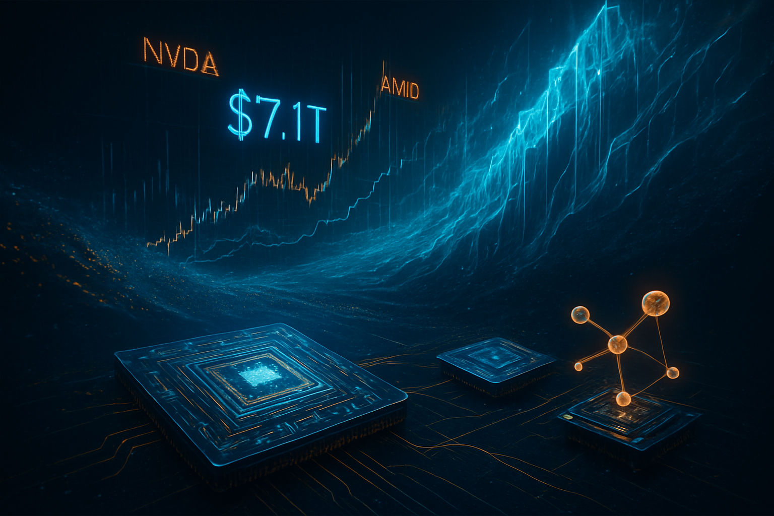
Tag: AI

  • Unlocking Hidden Histories: AI Transforms Black Press Archives with Schmidt Sciences Grant

    Unlocking Hidden Histories: AI Transforms Black Press Archives with Schmidt Sciences Grant

    In a groundbreaking move set to redefine the landscape of digital humanities and artificial intelligence, a significant initiative funded by Schmidt Sciences (a non-profit organization founded by Eric and Wendy Schmidt in 2024) is harnessing advanced AI to make the invaluable historical archives of the Black Press widely and freely accessible. The "Communities in the Loop: AI for Cultures & Contexts in Multimodal Archives" project, spearheaded by the University of California, Santa Barbara (UCSB), marks a pivotal moment, aiming to not only digitize fragmented historical documents but also to develop culturally competent AI that rectifies historical biases and empowers community participation. This $750,000 grant, part of an $11 million program for AI in humanities research, underscores a growing recognition of AI's potential to serve historical justice and democratize access to vital cultural heritage.

    The project's immediate significance lies in its dual objective: to unlock the rich narratives embedded in early African American newspapers—many of which have remained inaccessible or difficult to navigate—and to pioneer a new, ethical paradigm for AI development. By focusing on the Black Press, a cornerstone of African American intellectual and social life, the initiative promises to shed light on overlooked aspects of American history, providing scholars, genealogists, and the public with unprecedented access to primary sources that chronicle centuries of struggle, resilience, and advocacy. As of December 17, 2025, the project is actively underway, with a major public launch anticipated for Douglass Day 2027, marking the 200th anniversary of Freedom's Journal.

    Pioneering Culturally Competent AI for Historical Archives

    The "Communities in the Loop" project distinguishes itself through its innovative application of AI, specifically tailored to the unique challenges presented by historical Black Press archives. The core of the technical advancement lies in the development of specialized machine learning models for page layout segmentation and Optical Character Recognition (OCR). Unlike commercial AI tools, which often falter when confronted with the experimental layouts, varied fonts, and degraded print quality common in 19th-century newspapers, these custom models are being trained directly on Black press materials. This bespoke training is crucial for accurately identifying different content types and converting scanned images of text into machine-readable formats with significantly higher fidelity.

    Furthermore, the initiative is developing sophisticated AI-based methods to search and analyze both textual and visual content. This capability is particularly vital for uncovering "veiled protest and other political messaging" that early Black intellectuals often embedded in their publications to circumvent censorship and mitigate personal risk. By leveraging AI to detect nuanced patterns and contextual clues, researchers can identify covert forms of resistance and discourse that might be missed by conventional search methods.

    What truly sets this approach apart from previous technological endeavors is its "human in the loop" methodology. Recognizing the potential for AI to perpetuate existing biases if left unchecked, the project integrates human intelligence with AI through a collaborative process. Machine-generated text and analyses will be reviewed and improved by volunteers via the Zooniverse platform, a leading crowdsourcing platform. This iterative process not only ensures the accurate preservation of history but also serves to continuously train the AI to be more culturally competent, reduce biases, and reflect the nuances of the historical context. Initial reactions from the AI research community and digital humanities experts have been overwhelmingly positive, hailing the project as a model for ethical AI development that centers community involvement and historical justice, rather than relying on potentially biased "black box" algorithms.

    Reshaping the Landscape for AI Companies and Tech Giants

    The "Communities in the Loop" initiative, funded by Schmidt Sciences, carries significant implications for AI companies, tech giants, and startups alike. While the immediate beneficiaries include the University of California, Santa Barbara (UCSB), and its consortium of ten other universities and the Adler Planetarium, the broader impact will ripple through the AI industry. The project demonstrates a critical need for specialized, domain-specific AI solutions, particularly in fields where general-purpose AI models fall short due to data biases or complexity. This could spur a new wave of startups and research efforts focused on developing culturally competent AI and bespoke OCR technologies for niche historical or linguistic datasets.

    For major AI labs and tech companies, this initiative presents a competitive challenge and an opportunity. It underscores the limitations of their existing, often generalized, AI platforms when applied to highly specific and historically sensitive content. Companies like Alphabet (NASDAQ: GOOGL), Microsoft (NASDAQ: MSFT), and IBM (NYSE: IBM), which invest heavily in AI research and development, may be compelled to expand their focus on ethical AI, bias mitigation, and specialized training data for diverse cultural heritage projects. This could lead to the development of new product lines or services designed for archival research, digital humanities, and cultural preservation.

    The project also highlights a potential disruption to the assumption that off-the-shelf AI can universally handle all data types. It carves out a market for AI solutions that are not just powerful but also empathetic and contextually aware. Schmidt Sciences, as a non-profit funder, positions itself as a leader in fostering ethical and socially impactful AI development, potentially influencing other philanthropic organizations and venture capitalists to prioritize similar initiatives. This strategic advantage lies in demonstrating a viable, community-centric model for AI that is "not extractive, harmful, or discriminatory."

    A New Horizon for AI in the Broader Landscape

    This pioneering effort by Schmidt Sciences and UCSB fits squarely into the broader AI landscape as a powerful testament to the growing trend of "AI for good" and ethical AI development. It serves as a crucial case study demonstrating that AI can be a force for historical justice and cultural preservation, moving beyond its more commonly discussed applications in commerce or scientific research. By focusing on the Black Press, the project directly addresses historical underrepresentation and the digital divide in archival access, promoting a more inclusive understanding of history.

    The impacts are multifaceted: it increases the accessibility of vital historical documents, empowers communities to participate actively in the preservation and interpretation of their own histories, and sets a precedent for how AI can be developed in a transparent, accountable, and culturally sensitive manner. This initiative directly challenges the inherent biases often found in AI models trained on predominantly Western or mainstream datasets. By developing AI that understands the nuances of "veiled protest" and the complex sociopolitical context of the Black Press, it offers a powerful counter-narrative to the idea of AI as a neutral, objective tool, revealing its potential to uncover hidden truths.

    While the project actively works to mitigate concerns about bias through its "human in the loop" approach, it also highlights the ongoing need for vigilance in AI development. The broader application of AI in archives still necessitates careful consideration of data interpretation, the potential for new biases to emerge, and the indispensable role of human experts in guiding and validating AI outputs. This initiative stands as a significant milestone, comparable to earlier efforts in mass digitization, but elevated by its deep commitment to ethical AI and community engagement, pushing the boundaries of what AI can achieve in the humanities.

    The Road Ahead: Future Developments and Challenges

    Looking to the future, the "Communities in the Loop" project envisions several exciting developments. The most anticipated is the major public launch on Douglass Day 2027, which will coincide with the 200th anniversary of Freedom's Journal. This launch will include a new mobile interface, inviting widespread public participation in transcribing historical documents and further enriching the digital archive. This ongoing, collaborative effort promises to continuously refine the AI models, making them even more accurate and culturally competent over time.

    Beyond the Black Press, the methodologies and AI models developed through this grant hold immense potential for broader applications. This "human in the loop", culturally sensitive AI framework could be adapted to digitize and make accessible other marginalized archives, multilingual historical documents, or complex texts from diverse cultural contexts globally. Such applications could unlock vast troves of human history that are currently fragmented, inaccessible, or prone to misinterpretation by conventional AI.

    However, several challenges need to be addressed on the horizon. Sustaining high levels of volunteer engagement through platforms like Zooniverse will be crucial for the long-term success and accuracy of the project. Continual refinement of AI accuracy for the ever-diverse and often degraded content of historical materials remains an ongoing technical hurdle. Furthermore, ensuring the long-term digital preservation and accessibility of these newly digitized archives requires robust infrastructure and strategic planning. Experts predict that initiatives like this will catalyze a broader shift towards more specialized, ethically grounded, and community-driven AI applications within the humanities and cultural heritage sectors, setting a new standard for responsible technological advancement.

    A Landmark in Ethical AI and Digital Humanities

    The Schmidt Sciences Grant for Black Press archives represents a landmark development in both ethical artificial intelligence and the digital humanities. By committing substantial resources to a project that prioritizes historical justice, community participation, and the development of culturally competent AI, Schmidt Sciences (a non-profit founded by Eric and Wendy Schmidt in 2024) and the University of California, Santa Barbara, are setting a new benchmark for how technology can serve society. The "Communities in the Loop" initiative is not merely about digitizing old newspapers; it is about rectifying historical silences, empowering marginalized voices, and demonstrating AI's capacity to learn from and serve diverse communities.

    The significance of this development in AI history cannot be overstated. It underscores the critical importance of diverse training data, the perils of unexamined algorithmic bias, and the profound value of human expertise in guiding AI development. It offers a powerful counter-narrative to the often-dystopian anxieties surrounding AI, showcasing its potential as a tool for empathy, understanding, and social good. The project’s commitment to a "human in the loop" approach ensures that technology remains a servant to human values and historical accuracy.

    In the coming weeks and months, all eyes will be on the progress of the UCSB-led team as they continue to refine their AI models and engage with communities. The anticipation for the Douglass Day 2027 public launch, with its promise of a new mobile interface for widespread participation, will build steadily. This initiative serves as a powerful reminder that the future of AI is not solely about technical prowess but equally about ethical stewardship, cultural sensitivity, and its capacity to unlock and preserve the rich tapestry of human history.


    This content is intended for informational purposes only and represents analysis of current AI developments.

    TokenRing AI delivers enterprise-grade solutions for multi-agent AI workflow orchestration, AI-powered development tools, and seamless remote collaboration platforms.
    For more information, visit https://www.tokenring.ai/.

  • AI Fuels Memory Price Surge: A Double-Edged Sword for the Tech Industry

    AI Fuels Memory Price Surge: A Double-Edged Sword for the Tech Industry

    The global technology industry finds itself at a pivotal juncture, with the once-cyclical memory market now experiencing an unprecedented surge in prices and severe supply shortages. While conventional wisdom often links "stabilized" memory prices to a healthy tech sector, the current reality paints a different picture: rapidly escalating costs for DRAM and NAND flash chips, driven primarily by the insatiable demand from Artificial Intelligence (AI) applications. This dramatic shift, far from stabilization, serves as a potent economic indicator, revealing both the immense growth potential of AI and the significant cost pressures and strategic reorientations facing the broader tech landscape. The implications are profound, affecting everything from the profitability of device manufacturers to the timelines of critical digital infrastructure projects.

    This surge signals a robust, albeit concentrated, demand, primarily from the burgeoning AI sector, and a disciplined, strategic response from memory manufacturers. While memory producers like Micron Technology (NASDAQ: MU), Samsung Electronics (KRX: 005930), and SK Hynix (KRX: 000660) are poised for a multi-year upcycle, the rest of the tech ecosystem grapples with elevated component costs and potential delays. The dynamics of memory pricing, therefore, offer a nuanced lens through which to assess the true health and future trajectory of the technology industry, underscoring a market reshaped by the AI revolution.

    The AI Tsunami: Reshaping the Memory Landscape with Soaring Prices

    The current state of the memory market is characterized by a significant departure from any notion of "stabilization." Instead, contract prices for certain categories of DRAM and 3D NAND have reportedly doubled in a month, with overall memory prices projected to rise substantially through the first half of 2026, potentially doubling by mid-2026 compared to early 2025 levels. This explosive growth is largely attributed to the unprecedented demand for High-Bandwidth Memory (HBM) and next-generation server memory, critical components for AI accelerators and data centers.

    Technically, AI servers demand significantly more memory – often twice the total memory content and three times the DRAM content compared to traditional servers. Furthermore, the specialized HBM used in AI GPUs is not only more profitable but also actively consuming available wafer capacity. Memory manufacturers are strategically reallocating production from traditional, lower-margin DDR4 DRAM and conventional NAND towards these higher-margin, advanced memory solutions. This strategic pivot highlights the industry's response to the lucrative AI market, where the premium placed on performance and bandwidth outweighs cost considerations for key players. This differs significantly from previous market cycles where oversupply often led to price crashes; instead, disciplined capacity expansion and a targeted shift to high-value AI memory are driving the current price increases. Initial reactions from the AI research community and industry experts confirm this trend, with many acknowledging the necessity of high-performance memory for advanced AI workloads and anticipating continued demand.

    Navigating the Surge: Impact on Tech Giants, AI Innovators, and Startups

    The soaring memory prices and supply constraints create a complex competitive environment, benefiting some while challenging others. Memory manufacturers like Micron Technology (NASDAQ: MU), Samsung Electronics (KRX: 005930), and SK Hynix (KRX: 000660) are the primary beneficiaries. Their strategic shift towards HBM production and the overall increase in memory ASPs are driving improved profitability and a projected multi-year upcycle. Micron, in particular, is seen as a bellwether for the memory industry, with its rising share price reflecting elevated expectations for continued pricing improvement and AI-driven demand.

    Conversely, Original Equipment Manufacturers (OEMs) across various tech segments – from smartphone makers to PC vendors and even some cloud providers – face significant cost pressures. Elevated memory costs can squeeze profit margins or necessitate price increases for end products, potentially impacting consumer demand. Some smartphone manufacturers have already warned of possible price hikes of 20-30% by mid-2026. For AI startups and smaller tech companies, these rising costs could translate into higher operational expenses for their compute infrastructure, potentially slowing down innovation or increasing their need for capital. The competitive implications extend to major AI labs and tech giants like Google (NASDAQ: GOOGL), Microsoft (NASDAQ: MSFT), and Amazon (NASDAQ: AMZN), who are heavily investing in AI infrastructure. While their scale allows for better negotiation and strategic sourcing, they are not immune to the overall increase in component costs, which could affect their cloud service offerings and hardware development. The market is witnessing a strategic advantage for companies that have secured long-term supply agreements or possess in-house memory production capabilities.

    A Broader Economic Barometer: AI's Influence on Global Tech Trends

    The current memory market dynamics are more than just a component pricing issue; they are a significant barometer for the broader technology landscape and global economic trends. The intense demand for AI-specific memory underscores the massive capital expenditure flowing into AI infrastructure, signaling a profound shift in technological priorities. This fits into the broader AI landscape as a clear indicator of the industry's rapid maturation and its move from research to widespread application, particularly in data centers and enterprise solutions.

    The impacts are multi-faceted: it highlights the critical role of semiconductors in modern economies, exacerbates existing supply chain vulnerabilities, and puts upward pressure on the cost of digital transformation. The reallocation of wafer capacity to HBM means less output for conventional memory, potentially affecting sectors beyond AI and consumer electronics. Potential concerns include the risk of an "AI bubble" if demand were to suddenly contract, leaving manufacturers with overcapacity in specialized memory. This situation contrasts sharply with previous AI milestones where breakthroughs were often software-centric; today, the hardware bottleneck, particularly memory, is a defining characteristic of the current AI boom. Comparisons to past tech booms, such as the dot-com era, raise questions about sustainability, though the tangible infrastructure build-out for AI suggests a more fundamental demand driver.

    The Horizon: Sustained Demand, New Architectures, and Persistent Challenges

    Looking ahead, experts predict that the strong demand for high-performance memory, particularly HBM, will persist, driven by the continued expansion of AI capabilities and widespread adoption across industries. Near-term developments are expected to focus on further advancements in HBM generations (e.g., HBM3e, HBM4) with increased bandwidth and capacity, alongside innovations in packaging technologies to integrate memory more tightly with AI processors. Long-term, the industry may see the emergence of novel memory architectures designed specifically for AI workloads, such as Compute-in-Memory (CIM) or Processing-in-Memory (PIM), which aim to reduce data movement bottlenecks and improve energy efficiency.

    Potential applications on the horizon include more sophisticated edge AI devices, autonomous systems requiring real-time processing, and advancements in scientific computing and drug discovery, all heavily reliant on high-bandwidth, low-latency memory. However, significant challenges remain. Scaling manufacturing capacity for advanced memory technologies is complex and capital-intensive, with new fabrication plants taking at least three years to come online. This means substantial capacity increases won't be realized until late 2028 at the earliest, suggesting that supply constraints and elevated prices could persist for several years. Experts predict a continued focus on optimizing memory power consumption and developing more cost-effective production methods while navigating geopolitical complexities affecting semiconductor supply chains.

    A New Era for Memory: Fueling the AI Revolution

    The current surge in memory prices and the strategic shift in manufacturing priorities represent a watershed moment in the technology industry, profoundly shaped by the AI revolution. Far from stabilizing, memory prices are acting as a powerful indicator of intense, AI-driven demand, signaling a robust yet concentrated growth phase within the tech sector. Key takeaways include the immense profitability for memory manufacturers, the significant cost pressures on OEMs and other tech players, and the critical role of advanced memory in enabling next-generation AI.

    This development's significance in AI history cannot be overstated; it underscores the hardware-centric demands of modern AI, distinguishing it from prior, more software-focused milestones. The long-term impact will likely see a recalibration of tech company strategies, with greater emphasis on supply chain resilience and strategic partnerships for memory procurement. What to watch for in the coming weeks and months includes further announcements from memory manufacturers regarding capacity expansion, the financial results of OEMs reflecting the impact of higher memory costs, and any potential shifts in AI investment trends that could alter the demand landscape. The memory market, once a cyclical indicator, has now become a dynamic engine, directly fueling and reflecting the accelerating pace of the AI era.


    This content is intended for informational purposes only and represents analysis of current AI developments.

    TokenRing AI delivers enterprise-grade solutions for multi-agent AI workflow orchestration, AI-powered development tools, and seamless remote collaboration platforms.
    For more information, visit https://www.tokenring.ai/.

  • The Shrinking Giant: How Miniaturized Chips are Powering AI’s Next Revolution

    The Shrinking Giant: How Miniaturized Chips are Powering AI’s Next Revolution

    The relentless pursuit of smaller, more powerful, and energy-efficient chips is not just an incremental improvement; it's a fundamental imperative reshaping the entire technology landscape. As of December 2025, the semiconductor industry is at a pivotal juncture, where the continuous miniaturization of transistors, coupled with revolutionary advancements in advanced packaging, is driving an unprecedented surge in computational capabilities. This dual strategy is the backbone of modern artificial intelligence (AI), enabling breakthroughs in generative AI, high-performance computing (HPC), and pushing intelligence to the very edge of our devices. The ability to pack billions of transistors into microscopic spaces, and then ingeniously interconnect them, is fueling a new era of innovation, making smarter, faster, and more integrated technologies a reality.

    Technical Milestones in Miniaturization

    The current wave of chip miniaturization goes far beyond simply shrinking transistors; it involves fundamental architectural shifts and sophisticated integration techniques. Leading foundries are aggressively pushing into sub-3 nanometer (nm) process nodes. Taiwan Semiconductor Manufacturing Company (TSMC) (NYSE: TSM) is on track for volume production of its 2nm (N2) process in the second half of 2025, transitioning from FinFET to Gate-All-Around (GAA) nanosheet transistors. This shift offers superior control over electrical current, significantly reducing leakage and improving power efficiency. TSMC is also developing an A16 (1.6nm) process for late 2026, which will integrate nanosheet transistors with a novel Super Power Rail (SPR) solution for further performance and density gains.

    Similarly, Intel Corporation (NASDAQ: INTC) is advancing with its 18A (1.8nm) process, which is considered "ready" for customer projects with high-volume manufacturing expected by Q4 2025. Intel's 18A node leverages RibbonFET GAA technology and introduces PowerVia backside power delivery. PowerVia is a groundbreaking innovation that moves the power delivery network to the backside of the wafer, separating power and signal routing. This significantly improves density, reduces resistive power delivery droop, and enhances performance by freeing up routing space on the front side. Samsung Electronics (KRX: 005930) was the first to commercialize GAA transistors with its 3nm process and plans to launch its third generation of GAA technology (MBCFET) with its 2nm process in 2025, targeting mobile chips.

    Beyond traditional 2D scaling, 3D stacking and advanced packaging are becoming increasingly vital. Technologies like Through-Silicon Vias (TSVs) enable multiple layers of integrated circuits to be stacked and interconnected directly, drastically shortening interconnect lengths for faster signal transmission and lower power consumption. Hybrid bonding, connecting metal pads directly without copper bumps, allows for significantly higher interconnect density. Monolithic 3D integration, where layers are built sequentially, promises even denser vertical connections and has shown potential for 100- to 1,000-fold improvements in energy-delay product for AI workloads. These approaches represent a fundamental shift from monolithic System-on-Chip (SoC) designs, overcoming limitations in reticle size, manufacturing yields, and the "memory wall" by allowing for vertical integration and heterogeneous chiplet integration. Initial reactions from the AI research community and industry experts are overwhelmingly positive, viewing these advancements as critical enablers for the next generation of AI and high-performance computing, particularly for generative AI and large language models.

    Industry Shifts and Competitive Edge

    The profound implications of chip miniaturization and advanced packaging are reverberating across the entire tech industry, fundamentally altering competitive landscapes and market dynamics. AI companies stand to benefit immensely, as these technologies are crucial for faster processing, improved energy efficiency, and greater component integration essential for high-performance AI. Companies like NVIDIA Corporation (NASDAQ: NVDA) and Advanced Micro Devices (NASDAQ: AMD) are prime beneficiaries, leveraging 2.5D and 3D stacking with High Bandwidth Memory (HBM) to power their cutting-edge GPUs and AI accelerators, giving them a significant edge in the booming AI and HPC markets.

    Tech giants are strategically investing heavily in these advancements. Foundries like TSMC, Intel, and Samsung are not just manufacturers but integral partners, expanding their advanced packaging capacities (e.g., TSMC's CoWoS, Intel's EMIB, Samsung's I-Cube). Cloud providers such as Alphabet (NASDAQ: GOOGL) with its TPUs and Amazon.com, Inc. (NASDAQ: AMZN) with Graviton and Trainium chips, along with Microsoft Corporation (NASDAQ: MSFT) and its Azure Maia 100, are developing custom AI silicon optimized for their specific workloads, gaining superior performance-per-watt and cost efficiency. This trend highlights a move towards vertical integration, where hardware, software, and packaging are co-designed for maximum impact.

    For startups, advanced packaging and chiplet architectures present a dual scenario. On one hand, modular, chiplet-based designs can democratize chip design, allowing smaller players to innovate by integrating specialized chiplets without the prohibitive costs of designing an entire SoC from scratch. Companies like Silicon Box and DEEPX are securing significant funding in this space. On the other hand, startups face challenges related to chiplet interoperability and the rapid obsolescence of leading-edge chips. The primary disruption is a significant shift away from purely monolithic chip designs towards more modular, chiplet-based architectures. Companies that fail to embrace heterogeneous integration and advanced packaging risk being outmaneuvered, as the market for generative AI chips alone is projected to exceed $150 billion in 2025.

    AI's Broader Horizon

    The wider significance of chip miniaturization and advanced packaging extends far beyond mere technical specifications; it represents a foundational shift in the broader AI landscape and trends. These innovations are not just enabling AI's current capabilities but are critical for its future trajectory. The insatiable demand from generative AI and large language models (LLMs) is a primary catalyst, with advanced packaging, particularly in overcoming memory bottlenecks and delivering high bandwidth, being crucial for both training and inference of these complex models. This also facilitates the transition of AI from cloud-centric operations to edge devices, enabling powerful yet energy-efficient AI in smartphones, wearables, IoT sensors, and even miniature PCs capable of running LLMs locally.

    The impacts are profound, leading to enhanced performance, improved energy efficiency (drastically reducing energy required for data movement), and smaller form factors that push AI into new application domains. Radical miniaturization is enabling novel applications such as ultra-thin, wireless brain implants (like BISC) for brain-computer interfaces, advanced driver-assistance systems (ADAS) in autonomous vehicles, and even programmable microscopic robots for potential medical applications. This era marks a "symbiotic relationship between software and silicon," where hardware advancements are as critical as algorithmic breakthroughs. The economic impact is substantial, with the advanced packaging market for data center AI chips projected for explosive growth, from $5.6 billion in 2024 to $53.1 billion by 2030, a CAGR of over 40%.

    However, concerns persist. The manufacturing complexity and staggering costs of developing and producing advanced packaging and sub-2nm process nodes are immense. Thermal management in densely integrated packages remains a significant challenge, requiring innovative cooling solutions. Supply chain resilience is also a critical issue, with geopolitical concentration of advanced manufacturing creating vulnerabilities. Compared to previous AI milestones, which were often driven by algorithmic advancements (e.g., expert systems, machine learning, deep learning), the current phase is defined by hardware innovation that is extending and redefining Moore's Law, fundamentally overcoming the "memory wall" that has long hampered AI performance. This hardware-software synergy is foundational for the next generation of AI capabilities.

    The Road Ahead: Future Innovations

    Looking ahead, the future of chip miniaturization and advanced packaging promises even more radical transformations. In the near term, the industry will see the widespread adoption and refinement of 2nm and 1.8nm process nodes, alongside increasingly sophisticated 2.5D and 3D integration techniques. The push beyond 1nm will likely involve exploring novel transistor architectures and materials beyond silicon, such as carbon nanotube transistors (CNTs) and 2D materials like graphene, offering superior conductivity and minimal leakage. Advanced lithography, particularly High-NA EUV, will be crucial for pushing feature sizes below 10nm and enabling future 1.4nm nodes around 2027.

    Longer-term developments include the maturation of hybrid bonding for ultra-fine pitch vertical interconnects, crucial for next-generation High-Bandwidth Memory (HBM) beyond 16-Hi or 20-Hi layers. Co-Packaged Optics (CPO) will integrate optical interconnects directly into advanced packages, overcoming electrical bandwidth limitations for exascale AI systems. New interposer materials like glass are gaining traction due to superior electrical and thermal properties. Experts also predict the increasing integration of quantum computing components into the semiconductor ecosystem, leveraging established fabrication techniques for silicon-based qubits. Potential applications span more powerful and energy-efficient AI accelerators, robust solutions for 5G and 6G networks, hyper-miniaturized IoT sensors, advanced automotive systems, and groundbreaking medical technologies.

    Despite the exciting prospects, significant challenges remain. Physical limits at the sub-nanometer scale introduce quantum effects and extreme heat dissipation issues, demanding innovative thermal management solutions like microfluidic cooling or diamond materials. The escalating costs of advanced manufacturing, with new fabs costing tens of billions of dollars and High-NA EUV machines nearing $400 million, pose substantial economic hurdles. Manufacturing complexity, yield management for multi-die assemblies, and the immaturity of new material ecosystems are also critical challenges. Experts predict continued market growth driven by AI, a sustained "More than Moore" era where packaging is central, and a co-architected approach to chip design and packaging.

    A New Era of Intelligence

    In summary, the ongoing revolution in chip miniaturization and advanced packaging represents the most significant hardware transformation underpinning the current and future trajectory of Artificial Intelligence. Key takeaways include the transition to a "More-than-Moore" era, where advanced packaging is a core architectural enabler, not just a back-end process. This shift is fundamentally driven by the insatiable demands of generative AI and high-performance computing, which require unprecedented levels of computational power, memory bandwidth, and energy efficiency. These advancements are directly overcoming historical bottlenecks like the "memory wall," allowing AI models to grow in complexity and capability at an exponential rate.

    This development's significance in AI history cannot be overstated; it is the physical foundation upon which the next generation of intelligent systems will be built. It is enabling a future of ubiquitous and intelligent devices, where AI is seamlessly integrated into every facet of our lives, from autonomous vehicles to advanced medical implants. The long-term impact will be a world defined by co-architected designs, heterogeneous integration as the norm, and a relentless pursuit of sustainability in computing. The industry is witnessing a profound and enduring change, ensuring that the spirit of Moore's Law continues to drive progress, albeit through new and innovative means.

    In the coming weeks and months, watch for continued market growth in advanced packaging, particularly for AI-driven applications, with revenues projected to significantly outpace the rest of the chip industry. Keep an eye on the roadmaps of major AI chip developers like NVIDIA and AMD, as their next-generation architectures will define the capabilities of future AI systems. The maturation of novel packaging technologies such as panel-level packaging and hybrid bonding, alongside the further development of neuromorphic and photonic chips, will be critical indicators of progress. Finally, geopolitical factors and supply chain dynamics will continue to influence the availability and cost of these cutting-edge components, underscoring the strategic importance of semiconductor manufacturing in the global economy.


    This content is intended for informational purposes only and represents analysis of current AI developments.

    TokenRing AI delivers enterprise-grade solutions for multi-agent AI workflow orchestration, AI-powered development tools, and seamless remote collaboration platforms.
    For more information, visit https://www.tokenring.ai/.

  • The Unseen Battleground: How Semiconductor Supply Chain Vulnerabilities Threaten Global Tech and AI

    The Unseen Battleground: How Semiconductor Supply Chain Vulnerabilities Threaten Global Tech and AI

    The global semiconductor supply chain, an intricate and highly specialized network spanning continents, has emerged as a critical point of vulnerability for the world's technological infrastructure. Far from being a mere industrial concern, the interconnectedness of chip manufacturing, its inherent weaknesses, and ongoing efforts to build resilience are profoundly reshaping geopolitics, economic stability, and the very future of artificial intelligence. Recent years have laid bare the fragility of this essential ecosystem, prompting an unprecedented global scramble to de-risk and diversify a supply chain that underpinning nearly every aspect of modern life.

    This complex web, where components for a single chip can travel tens of thousands of miles before reaching their final destination, has long been optimized for efficiency and cost. However, events ranging from natural disasters to escalating geopolitical tensions have exposed its brittle nature, transforming semiconductors from commercial commodities into strategic assets. The consequences are far-reaching, impacting everything from the production of smartphones and cars to the advancement of cutting-edge AI, demanding a fundamental re-evaluation of how the world produces and secures its digital foundations.

    The Global Foundry Model: A Double-Edged Sword of Specialization

    The semiconductor manufacturing process is a marvel of modern engineering, yet its global distribution and extreme specialization create a delicate balance. The journey begins with design and R&D, largely dominated by companies in the United States and Europe. Critical materials and equipment follow, with nations like Japan supplying ultrapure silicon wafers and the Netherlands, through ASML (AMS:ASML), holding a near-monopoly on extreme ultraviolet (EUV) lithography systems—essential for advanced chip production.

    The most capital-intensive and technologically demanding stage, front-end fabrication (wafer fabs), is overwhelmingly concentrated in East Asia. Taiwan Semiconductor Manufacturing Company (NYSE:TSM), or TSMC, alone accounts for over 60% of global fabrication capacity and an astounding 92% of the world's most advanced chips (below 10 nanometers), with Samsung Electronics (KRX:005930) in South Korea contributing another 8%. The back-end assembly, testing, and packaging (ATP) stage is similarly concentrated, with 95% of facilities in the Indo-Pacific region. This "foundry model," while driving incredible innovation and efficiency, means that a disruption in a single geographic chokepoint can send shockwaves across the globe. Initial reactions from the AI research community and industry experts highlight that this extreme specialization, once lauded for its efficiency, is now seen as the industry's Achilles' heel, demanding urgent structural changes.

    Reshaping the Tech Landscape: From Giants to Startups

    The vulnerabilities within the semiconductor supply chain have profound and varied impacts across the tech industry, fundamentally reshaping competitive dynamics for AI companies, tech giants, and startups alike. Major tech companies like Apple (NASDAQ:AAPL), Microsoft (NASDAQ:MSFT), Alphabet (NASDAQ:GOOGL), and Amazon (NASDAQ:AMZN) are heavily reliant on a steady supply of advanced chips for their cloud services, data centers, and consumer products. Their ability to diversify sourcing, invest directly in in-house chip design (e.g., Apple's M-series, Google's TPUs, Amazon's Inferentia), and form strategic partnerships with foundries gives them a significant advantage in securing capacity. However, even these giants face increased costs, longer lead times, and the complex challenge of navigating a fragmented procurement environment influenced by nationalistic preferences.

    AI labs and startups, on the other hand, are particularly vulnerable. With fewer resources and less purchasing power, they struggle to procure essential high-performance GPUs and specialized AI accelerators, leading to increased component costs, delayed product development, and higher barriers to entry. This environment could lead to a consolidation of AI development around well-resourced players, potentially stifling innovation from smaller, agile firms. Conversely, the global push for regionalization and government incentives, such as the U.S. CHIPS Act, could create opportunities for new domestic semiconductor design and manufacturing startups, fostering localized innovation ecosystems. Companies like NVIDIA (NASDAQ:NVDA), TSMC, Samsung, Intel (NASDAQ:INTC), and AMD (NASDAQ:AMD) stand to benefit from increased demand and investment in their manufacturing capabilities, while equipment providers like ASML remain indispensable. The competitive landscape is shifting from pure cost efficiency to supply chain resilience, with vertical integration and geopolitical agility becoming key strategic advantages.

    Beyond the Chip: Geopolitics, National Security, and the AI Race

    The wider significance of semiconductor supply chain vulnerabilities extends far beyond industrial concerns, touching upon national security, economic stability, and the very trajectory of the AI revolution. Semiconductors are now recognized as strategic assets, foundational to defense systems, 5G networks, quantum computing, and the advanced AI systems that will define future global power dynamics. The concentration of advanced chip manufacturing in geopolitically sensitive regions, particularly Taiwan, creates a critical national security vulnerability, with some experts warning that "the next war will not be fought over oil, it will be fought over silicon."

    The 2020-2023 global chip shortage, exacerbated by the COVID-19 pandemic, served as a stark preview of this risk, costing the automotive industry an estimated $500 billion and the U.S. economy $240 billion in 2021. This crisis underscored how disruptions can trigger cascading failures across interconnected industries, impacting personal livelihoods and the pace of digital transformation. Compared to previous industrial milestones, the semiconductor industry's unique "foundry model" has led to an unprecedented level of concentration for such a universally critical component, creating a single point of failure unlike anything seen in past industrial revolutions. This situation has elevated supply chain resilience to a foundational element for continued technological progress, making it a central theme in international relations and a driving force behind a new era of industrial policy focused on security over pure efficiency.

    Forging a Resilient Future: Regionalization, AI, and New Architectures

    Looking ahead, the semiconductor industry is bracing for a period of transformative change aimed at forging a more resilient and diversified future. In the near term (1-3 years), aggressive global investment in new fabrication plants (fabs) is the dominant trend, driven by initiatives like the US CHIPS and Science Act ($52.7 billion) and the European Chips Act (€43 billion). These efforts aim to rebalance global production and reduce dependency on concentrated regions, leading to a significant push for "reshoring" and "friend-shoring" strategies. Enhanced supply chain visibility, powered by AI-driven forecasting and data analytics, will also be crucial for real-time risk management and compliance.

    Longer term (3+ years), experts predict a further fragmentation into more regionalized manufacturing ecosystems, potentially requiring companies to tailor chip designs for specific markets. Innovations like "chiplets," which break down complex chips into smaller, interconnected modules, offer greater design and sourcing flexibility. The industry will also explore new materials (e.g., gallium nitride, silicon carbide) and advanced packaging technologies to boost performance and efficiency. However, significant challenges remain, including persistent geopolitical tensions, the astronomical costs of building new fabs (up to $20 billion for a sub-3nm facility), and a global shortage of skilled talent. Despite these hurdles, the demand for AI, data centers, and memory technologies is expected to drive the semiconductor market to become a trillion-dollar industry by 2030, with AI chips alone exceeding $150 billion in 2025. Experts predict that resilience, diversification, and long-term planning will be the new guiding principles, with AI playing a dual role—both as a primary driver of chip demand and as a critical tool for optimizing the supply chain itself.

    A New Era of Strategic Imperatives for the Digital Age

    The global semiconductor supply chain stands at a pivotal juncture, its inherent interconnectedness now recognized as both its greatest strength and its most profound vulnerability. The past few years have served as an undeniable wake-up call, demonstrating how disruptions in this highly specialized ecosystem can trigger widespread economic losses, impede technological progress, and pose serious national security threats. The concerted global response, characterized by massive government incentives and private sector investments in regionalized manufacturing, strategic stockpiling, and advanced analytics, marks a fundamental shift away from pure cost efficiency towards resilience and security.

    This reorientation holds immense significance for the future of AI and technological advancement. Reliable access to advanced chips is no longer merely a commercial advantage but a strategic imperative, directly influencing the pace and scalability of AI innovation. While complete national self-sufficiency remains economically impractical, the long-term impact will likely see a more diversified, albeit still globally interconnected, manufacturing landscape. In the coming weeks and months, critical areas to watch include the progress of new fab construction, shifts in geopolitical trade policies, the dynamic between AI chip demand and supply, and the effectiveness of initiatives to address the global talent shortage. The ongoing transformation of the semiconductor supply chain is not just an industry story; it is a defining narrative of the 21st century, shaping the contours of global power and the future of our digital world.


    This content is intended for informational purposes only and represents analysis of current AI developments.

    TokenRing AI delivers enterprise-grade solutions for multi-agent AI workflow orchestration, AI-powered development tools, and seamless remote collaboration platforms.
    For more information, visit https://www.tokenring.ai/.

  • Bridging the Chasm: How Academic-Industry Collaboration Fuels Semiconductor Innovation for the AI Era

    Bridging the Chasm: How Academic-Industry Collaboration Fuels Semiconductor Innovation for the AI Era

    In the rapidly accelerating landscape of artificial intelligence, the very foundation upon which AI thrives – semiconductor technology – is undergoing a profound transformation. This evolution isn't happening in isolation; it's the direct result of a dynamic and indispensable partnership between academic research institutions and the global semiconductor industry. This critical synergy translates groundbreaking scientific discoveries into tangible technological advancements, driving the next wave of AI capabilities and cementing the future of modern computing. As of December 2025, this collaborative ecosystem is more vital than ever, accelerating innovation, cultivating a specialized workforce, and shaping the competitive dynamics of the tech world.

    From Lab Bench to Chip Fab: A Technical Deep Dive into Collaborative Breakthroughs

    The journey from a theoretical concept in a university lab to a mass-produced semiconductor powering an AI application is often paved by academic-industry collaboration. These partnerships have been instrumental in overcoming fundamental physical limitations and introducing revolutionary architectures.

    One such pivotal advancement is High-k Metal Gate (HKMG) Technology. For decades, silicon dioxide (SiO2) served as the gate dielectric in transistors. However, as transistors shrank to the nanometer scale, SiO2 became too thin, leading to excessive leakage currents and thermal inefficiencies. Academic research, followed by intense industry collaboration, led to the adoption of high-k materials (like hafnium-based dielectrics) and metal gates. This innovation, first commercialized by Intel (NASDAQ: INTC) in its 45nm microprocessors in 2007, dramatically reduced gate leakage current by over 30 times and improved power consumption by approximately 40%. It allowed for a physically thicker insulator that was electrically equivalent to a much thinner SiO2 layer, thus re-enabling transistor scaling and solving issues like Fermi-level pinning. Initial reactions from industry, while acknowledging the complexity and cost, recognized HKMG as a necessary and transformative step to "restart chip scaling."

    Another monumental shift came with Fin Field-Effect Transistors (FinFETs). Traditional planar transistors struggled with short-channel effects as their dimensions decreased, leading to poor gate control and increased leakage. Academic research, notably from UC Berkeley in 1999, demonstrated the concept of multi-gate transistors where the gate wraps around a raised silicon "fin." This 3D architecture, commercialized by Intel (NASDAQ: INTC) at its 22nm node in 2011, offers superior electrostatic control, significantly reducing leakage current, lowering power consumption, and improving switching speeds. FinFETs effectively extended Moore's Law, becoming the cornerstone of advanced CPUs, GPUs, and SoCs in modern smartphones and high-performance computing. Foundries like TSMC (NYSE: TSM) later adopted FinFETs and even launched university programs to foster further innovation and talent in this area, solidifying its position as the "first significant architectural shift in transistor device history."

    Beyond silicon, Wide Bandgap (WBG) Semiconductors, such as Gallium Nitride (GaN) and Silicon Carbide (SiC), represent another area of profound academic-industry impact. These materials boast wider bandgaps, higher electron mobility, and superior thermal conductivity compared to silicon, allowing devices to operate at much higher voltages, frequencies, and temperatures with significantly reduced energy losses. GaN-based LEDs, for example, revolutionized energy-efficient lighting and are now crucial for 5G base stations and fast chargers. SiC, meanwhile, is indispensable for electric vehicles (EVs), enabling high-efficiency onboard chargers and traction inverters, and is critical for renewable energy infrastructure. Academic research laid the groundwork for crystal growth and device fabrication, with industry leaders like STMicroelectronics (NYSE: STM) now introducing advanced generations of SiC MOSFET technology, driving breakthroughs in power efficiency for automotive and industrial applications.

    Emerging academic breakthroughs, such as Neuromorphic Computing Architectures and Novel Non-Volatile Memory (NVM) Technologies, are poised to redefine AI hardware. Researchers are developing molecular memristors and single silicon transistors that mimic biological neurons and synapses, aiming to overcome the Von Neumann bottleneck by integrating memory and computation. This "in-memory computing" promises to drastically reduce energy consumption for AI workloads, enabling powerful AI on edge devices. Similarly, next-generation NVMs like Phase-Change Memory (PCM) and Resistive Random-Access Memory (ReRAM) are being developed to combine the speed of SRAM, the density of DRAM, and the non-volatility of Flash, crucial for data-intensive AI and the Internet of Things (IoT). These innovations, often born from university research, are recognized as "game-changers" for the "global AI race."

    Corporate Chessboard: Shifting Dynamics in the AI Hardware Race

    The intensified collaboration between academia and industry is profoundly reshaping the competitive landscape for major AI companies, tech giants, and startups alike. It's a strategic imperative for staying ahead in the "AI supercycle."

    Major AI Companies and Tech Giants like IBM (NYSE: IBM), Google (NASDAQ: GOOGL), Amazon (NASDAQ: AMZN), Microsoft (NASDAQ: MSFT), NVIDIA (NASDAQ: NVDA), Intel (NASDAQ: INTC), and AMD (NASDAQ: AMD) are direct beneficiaries. These companies gain early access to pioneering research, allowing them to accelerate the design and production of next-generation AI chips. Google's custom Tensor Processing Units (TPUs) and Amazon's Graviton and AI/ML chips, for instance, are outcomes of such deep engagements, optimizing their massive cloud infrastructures for AI workloads and reducing reliance on external suppliers. NVIDIA (NASDAQ: NVDA), a dominant force in AI GPUs, consistently invests in academic research and fosters an ecosystem that benefits from university-driven advancements in parallel computing and AI algorithms.

    Semiconductor Foundries and Advanced Packaging Service Providers such as TSMC (NYSE: TSM), Samsung (KRX: 005930), and Amkor Technology (NASDAQ: AMKR) also see immense benefits. Innovations in advanced packaging, new materials, and fabrication techniques directly translate into new manufacturing capabilities and increased demand for their specialized services, underpinning the production of high-performance AI accelerators.

    Startups in the AI hardware space leverage these collaborations to access foundational technologies, specialized talent, and critical resources that would otherwise be out of reach. Incubators and programs, often linked to academic institutions, provide mentorship and connections, enabling early-stage companies to develop niche AI hardware solutions and potentially disrupt traditional markets. Companies like Cerebras Systems and Graphcore, focused on AI-dedicated chips, exemplify how startups can attract significant investment by developing highly optimized solutions.

    The competitive implications are significant. Accelerated innovation and shorter time-to-market are crucial in the rapidly evolving AI landscape. Companies capable of developing proprietary custom silicon solutions, optimized for specific AI workloads, gain a critical edge in areas like large language models and autonomous driving. This also fuels the shift from general-purpose CPUs and GPUs to specialized AI hardware, potentially disrupting existing product lines. Furthermore, advancements like optical interconnects and open-source architectures (e.g., RISC-V), often championed by academic research, could lead to new, cost-effective solutions that challenge established players. Strategic advantages include technological leadership, enhanced supply chain resilience through "reshoring" efforts (e.g., the U.S. CHIPS Act), intellectual property (IP) gains, and vertical integration where tech giants design their own chips to optimize their cloud services.

    The Broader Canvas: AI, Semiconductors, and Society

    The wider significance of academic-industry collaboration in semiconductors for AI extends far beyond corporate balance sheets, profoundly influencing the broader AI landscape, national security, and even ethical considerations. As of December 2025, AI is the primary catalyst driving growth across the entire semiconductor industry, demanding increasingly sophisticated, efficient, and specialized chips.

    This collaborative model fits perfectly into current AI trends: the insatiable demand for specialized AI hardware (GPUs, TPUs, NPUs), the critical role of advanced packaging and 3D integration for performance and power efficiency, and the imperative for energy-efficient and low-power AI, especially for edge devices. AI itself is increasingly being used within the semiconductor industry to shorten design cycles and optimize chip architectures, creating a powerful feedback loop.

    The impacts are transformative. Joint efforts lead to revolutionary advancements like new 3D chip architectures projected to achieve "1,000-fold hardware performance improvements." This fuels significant economic growth, as seen by the semiconductor industry's confidence, with 93% of industry leaders expecting revenue growth in 2026. Moreover, AI's application in semiconductor design is cutting R&D costs by up to 26% and shortening time-to-market by 28%. Ultimately, this broader adoption of AI across industries, from telecommunications to healthcare, leads to more intelligent devices and robust data centers.

    However, significant concerns remain. Intellectual Property (IP) is a major challenge, requiring clear joint protocols beyond basic NDAs to prevent competitive erosion. National Security is paramount, as a reliable and secure semiconductor supply chain is vital for defense and critical infrastructure. Geopolitical risks and the geographic concentration of manufacturing are top concerns, prompting "re-shoring" efforts and international partnerships (like the US-Japan Upwards program). Ethical Considerations are also increasingly scrutinized. The development of AI-driven semiconductors raises questions about potential biases in chips, the accountability of AI-driven decisions in design, and the broader societal impacts of advanced AI, such as job displacement. Establishing clear ethical guidelines and ensuring explainable AI are critical.

    Compared to previous AI milestones, the current era is unique. While academic-industry collaborations in semiconductors have a long history (dating back to the transistor at Bell Labs), today's urgency and scale are unprecedented due to AI's transformative power. Hardware is no longer a secondary consideration; it's a primary driver, with AI development actively inspiring breakthroughs in semiconductor design. The relationship is symbiotic, moving beyond brute-force compute towards more heterogeneous and flexible architectures. Furthermore, unlike previous tech hypes, the current AI boom has spurred intense ethical scrutiny, making these considerations integral to the development of AI hardware.

    The Horizon: What's Next for Collaborative Semiconductor Innovation

    Looking ahead, academic-industry collaboration in semiconductor innovation for AI is poised for even greater integration and impact, driving both near-term refinements and long-term paradigm shifts.

    In the near term (1-5 years), expect a surge in specialized research facilities, like UT Austin's Texas Institute for Electronics (TIE), focusing on advanced packaging (e.g., 3D heterogeneous integration) and serving as national R&D hubs. The development of specialized AI hardware will intensify, including silicon photonics for ultra-low power edge devices and AI-driven manufacturing processes to enhance efficiency and security, as seen in the Siemens (ETR: SIE) and GlobalFoundries (NASDAQ: GFS) partnership. Advanced packaging techniques like 3D stacking and chiplet integration will be critical to overcome traditional scaling limitations, alongside the continued demand for high-performance GPUs and NPUs for generative AI.

    The long term (beyond 5 years) will likely see the continued pursuit of novel computing architectures, including quantum computing and neuromorphic chips designed to mimic the human brain's efficiency. The vision of "codable" hardware, where software can dynamically define silicon functions, represents a significant departure from current rigid hardware designs. Sustainable manufacturing and energy efficiency will become core drivers, pushing innovations in green computing, eco-friendly materials, and advanced cooling solutions. Experts predict the commercial emergence of optical and physics-native computing, moving from labs to practical applications in solving complex scientific simulations, and exponential performance gains from new 3D chip architectures, potentially achieving 100- to 1,000-fold improvements in energy-delay product.

    These advancements will unlock a plethora of potential applications. Data centers will become even more power-efficient, enabling the training of increasingly complex AI models. Edge AI devices will proliferate in industrial IoT, autonomous drones, robotics, and smart mobility. Healthcare will benefit from real-time diagnostics and advanced medical imaging. Autonomous systems, from ADAS to EVs, will rely on sophisticated semiconductor solutions. Telecommunications will see support for 5G and future wireless technologies, while finance will leverage low-latency accelerators for fraud detection and algorithmic trading.

    However, significant challenges must be addressed. A severe talent shortage remains the top concern, requiring continuous investment in STEM education and multi-disciplinary training. The high costs of innovation create barriers, particularly for academic institutions and smaller enterprises. AI's rapidly increasing energy footprint necessitates a focus on green computing. Technical complexity, including managing advanced packaging and heat generation, continues to grow. The pace of innovation mismatch between fast-evolving AI models and slower hardware development cycles can create bottlenecks. Finally, bridging the inherent academia-industry gap – reconciling differing objectives, navigating IP issues, and overcoming communication gaps – is crucial for maximizing collaborative potential.

    Experts predict a future of deepened collaboration between universities, companies, and governments to address talent shortages and foster innovation. The focus will increasingly be on hardware-centric AI, with a necessary rebalancing of investment towards AI infrastructure and "deep tech" hardware. New computing paradigms, including optical and physics-native computing, are expected to emerge. Sustainability will become a core driver, and AI tools will become indispensable for chip design and manufacturing automation. The trend towards specialized and flexible hardware will continue, alongside intensified efforts to enhance supply chain resilience and navigate increasing regulation and ethical considerations around AI.

    The Collaborative Imperative: A Look Ahead

    In summary, academic-industry collaboration in semiconductor innovation is not merely beneficial; it is the indispensable engine driving the current and future trajectory of Artificial Intelligence. These partnerships are the crucible where foundational science meets practical engineering, transforming theoretical breakthroughs into the powerful, efficient, and specialized chips that enable the most advanced AI systems. From the foundational shifts of HKMG and FinFETs to the emerging promise of neuromorphic computing and novel non-volatile memories, this synergy has consistently pushed the boundaries of what's possible in computing.

    The significance of this collaborative model in AI history cannot be overstated. It ensures that hardware advancements keep pace with, and actively inspire, the exponential growth of AI models, preventing computational bottlenecks from hindering progress. It's a symbiotic relationship where AI helps design better chips, and better chips unlock more powerful AI. The long-term impact will be a world permeated by increasingly intelligent, energy-efficient, and specialized AI, touching every facet of human endeavor.

    In the coming weeks and months, watch for continued aggressive investments by hyperscalers in AI infrastructure, particularly in advanced packaging and High Bandwidth Memory (HBM). The proliferation of "AI PCs" and GenAI smartphones will accelerate, pushing AI capabilities to the edge. Innovations in cooling solutions for increasingly power-dense AI data centers will be critical. Pay close attention to new government-backed initiatives and research hubs, like Purdue University's Institute of CHIPS and AI, and further advancements in generative AI tools for chip design automation. Finally, keep an eye on early-stage breakthroughs in novel compute paradigms like neuromorphic and quantum computing, as these will be the next frontiers forged through robust academic-industry collaboration. The future of AI is being built, one collaborative chip at a time.


    This content is intended for informational purposes only and represents analysis of current AI developments.

    TokenRing AI delivers enterprise-grade solutions for multi-agent AI workflow orchestration, AI-powered development tools, and seamless remote collaboration platforms.
    For more information, visit https://www.tokenring.ai/.

  • America’s Chip Renaissance: A New Era of Domestic Semiconductor Manufacturing Dawns

    America’s Chip Renaissance: A New Era of Domestic Semiconductor Manufacturing Dawns

    The United States is witnessing a profound resurgence in domestic semiconductor manufacturing, a strategic pivot driven by a confluence of geopolitical imperatives, economic resilience, and a renewed commitment to technological sovereignty. This transformative shift, largely catalyzed by comprehensive government initiatives like the CHIPS and Science Act, marks a critical turning point for the nation's industrial landscape and its standing in the global tech arena. The immediate significance of this renaissance is multi-faceted, promising enhanced supply chain security, a bolstering of national defense capabilities, and the creation of a robust ecosystem for future AI and advanced technology development.

    This ambitious endeavor seeks to reverse decades of offshoring and re-establish the US as a powerhouse in chip production. The aim is to mitigate vulnerabilities exposed by recent global disruptions and geopolitical tensions, ensuring a stable and secure supply of the advanced semiconductors that power everything from consumer electronics to cutting-edge AI systems and defense technologies. The implications extend far beyond mere economic gains, touching upon national security, technological leadership, and the very fabric of future innovation.

    The CHIPS Act: Fueling a New Generation of Fabs

    The cornerstone of America's semiconductor resurgence is the CHIPS and Science Act of 2022, a landmark piece of legislation that has unleashed an unprecedented wave of investment and development in domestic chip production. This act authorizes approximately $280 billion in new funding, with a dedicated $52.7 billion specifically earmarked for semiconductor manufacturing incentives, research and development (R&D), and workforce training. This substantial financial commitment is designed to make the US a globally competitive location for chip fabrication, directly addressing the higher costs previously associated with domestic production.

    Specifically, $39 billion is allocated for direct financial incentives, including grants, cooperative agreements, and loan guarantees, to companies establishing, expanding, or modernizing semiconductor fabrication facilities (fabs) within the US. Additionally, a crucial 25% investment tax credit for qualifying expenses related to semiconductor manufacturing property further sweetens the deal for investors. Since the Act's signing, companies have committed over $450 billion in private investments across 28 states, signaling a robust industry response. Major players like Intel (NASDAQ: INTC), Samsung (KRX: 005930), and Taiwan Semiconductor Manufacturing Company (TSMC) (NYSE: TSM) are at the forefront of this investment spree, announcing multi-billion dollar projects for new fabs capable of producing advanced logic and memory chips. The US is projected to more than triple its semiconductor manufacturing capacity from 2022 to 2032, a growth rate unmatched globally.

    This approach significantly differs from previous, more hands-off industrial policies. The CHIPS Act represents a direct, strategic intervention by the government to reshape a critical industry, moving away from reliance on market forces alone to ensure national security and economic competitiveness. Initial reactions from the AI research community and industry experts have been largely positive, recognizing the strategic importance of a secure and localized supply of advanced chips. The ability to innovate rapidly in AI relies heavily on access to cutting-edge silicon, and a domestic supply chain reduces both lead times and geopolitical risks. However, some concerns persist regarding the long-term sustainability of such large-scale government intervention and the potential for a talent gap in the highly specialized workforce required for advanced chip manufacturing. The Act also includes geographical restrictions, prohibiting funding recipients from expanding semiconductor manufacturing in countries deemed national security threats, with limited exceptions, further solidifying the strategic intent behind the initiative.

    Redrawing the AI Landscape: Implications for Tech Giants and Nimble Startups

    The strategic resurgence of US domestic chip production, powered by the CHIPS Act, is poised to fundamentally redraw the competitive landscape for artificial intelligence companies, from established tech giants to burgeoning startups. At its core, the initiative promises a more stable, secure, and geographically proximate supply of advanced semiconductors – the indispensable bedrock for all AI development and deployment. This stability is critical for accelerating AI research and development, ensuring consistent access to the cutting-edge silicon needed to train increasingly complex and data-intensive AI models.

    For tech giants like Alphabet (NASDAQ: GOOGL), Amazon (NASDAQ: AMZN), Microsoft (NASDAQ: MSFT), and Meta Platforms (NASDAQ: META), who are simultaneously hyperscale cloud providers and massive investors in AI infrastructure, the CHIPS Act provides a crucial domestic foundation. Many of these companies are already designing their own custom AI Application-Specific Integrated Circuits (ASICs) to optimize performance, cost, and supply chain control. Increased domestic manufacturing capacity directly supports these in-house chip design efforts, potentially granting them a significant competitive advantage. Semiconductor manufacturing leaders such as NVIDIA (NASDAQ: NVDA), the dominant force in AI GPUs, and Intel (NASDAQ: INTC), with its ambitious foundry expansion plans, stand as direct beneficiaries, poised for increased demand and investment opportunities.

    AI startups, often resource-constrained but innovation-driven, also stand to gain substantially. The CHIPS Act funnels billions into R&D for emerging technologies, including AI, providing access to funding and resources that were previously more accessible only to larger corporations. Startups that either contribute to the semiconductor supply chain (e.g., specialized equipment, materials) or develop AI solutions requiring advanced chips can leverage grants to scale their domestic operations. Furthermore, the Act's investment in education and workforce development programs aims to cultivate a larger talent pool of skilled engineers and technicians, a vital resource for new firms grappling with talent shortages. Initiatives like the National Semiconductor Technology Center (NSTC) are designed to foster collaboration, prototyping, and knowledge transfer, creating an ecosystem conducive to startup growth.

    However, this shift also introduces competitive pressures and potential disruptions. The trend of hyperscalers developing custom silicon could disrupt traditional semiconductor vendors primarily offering standard products. While largely beneficial, the high cost of domestic production compared to Asian counterparts raises questions about long-term sustainability without sustained incentives. Moreover, the immense capital requirements and technical complexity of advanced fabrication plants mean that only a handful of nations and companies can realistically compete at the leading edge, potentially leading to a consolidation of advanced chip manufacturing capabilities globally, albeit with a stronger emphasis on regional diversification. The Act's aim to significantly increase the US share of global semiconductor manufacturing, particularly for leading-edge chips, from near zero to 30% by August 2024, underscores a strategic repositioning to regain and secure leadership in a critical technological domain.

    A Geopolitical Chessboard: The Wider Significance of Silicon Sovereignty

    The resurgence of US domestic chip production transcends mere economic revitalization; it represents a profound strategic recalibration with far-reaching implications for the broader AI landscape and global technological power dynamics. This concerted effort, epitomized by the CHIPS and Science Act, is a direct response to the vulnerabilities exposed by a highly concentrated global semiconductor supply chain, where an overwhelming 75% of manufacturing capacity resides in China and East Asia, and 100% of advanced chip production is confined to Taiwan and South Korea. By re-shoring manufacturing, the US aims to secure its economic future, bolster national security, and solidify its position as a global leader in AI innovation.

    The impacts are multifaceted. Economically, the initiative has spurred over $500 billion in private sector commitments by July 2025, with significant investments from industry titans such as GlobalFoundries (NASDAQ: GFS), TSMC (NYSE: TSM), Samsung (KRX: 005930), and Micron Technology (NASDAQ: MU). This investment surge is projected to increase US semiconductor R&D spending by 25% by 2025, driving job creation and fostering a vibrant innovation ecosystem. From a national security perspective, advanced semiconductors are deemed critical infrastructure. The US strategy involves not only securing its own supply but also strategically restricting adversaries' access to cutting-edge AI chips and the means to produce them, as evidenced by initiatives like the "Chip Security Act of 2023" and partnerships such as Pax Silica with trusted allies. This ensures that the foundational hardware for critical AI systems, from defense applications to healthcare, remains secure and accessible.

    However, this ambitious undertaking is not without its concerns and challenges. Cost competitiveness remains a significant hurdle; manufacturing chips in the US is inherently more expensive than in Asia, a reality acknowledged by industry leaders like Morris Chang, founder of TSMC. A substantial workforce shortage, with an estimated need for an additional 100,000 engineers by 2030, poses another critical challenge. Geopolitical complexities also loom large, as aggressive trade policies and export controls, while aimed at strengthening the US position, risk fragmenting global technology standards and potentially alienating allies. Furthermore, the immense energy demands of advanced chip manufacturing facilities and AI-powered data centers raise significant questions about sustainable energy procurement.

    Comparing this era to previous AI milestones reveals a distinct shift. While earlier breakthroughs often centered on software and algorithmic advancements (e.g., the deep learning revolution, large language models), the current phase is fundamentally a hardware-centric revolution. It underscores an unprecedented interdependence between hardware and software, where specialized AI chip design is paramount for optimizing complex AI models. Crucially, semiconductor dominance has become a central issue in international relations, elevating control over the silicon supply chain to a determinant of national power in an AI-driven global economy. This geopolitical centrality marks a departure from earlier AI eras, where hardware considerations, while important, were not as deeply intertwined with national security and global influence.

    The Road Ahead: Future Developments and AI's Silicon Horizon

    The ambitious push for US domestic chip production sets the stage for a dynamic future, marked by rapid advancements and strategic realignments, all deeply intertwined with the trajectory of artificial intelligence. In the near term, the landscape will be dominated by the continued surge in investments and the materialization of new fabrication plants (fabs) across the nation. The CHIPS and Science Act, a powerful catalyst, has already spurred over $450 billion in private investments, leading to the construction of state-of-the-art facilities by industry giants like Intel (NASDAQ: INTC), TSMC (NYSE: TSM), and Samsung (KRX: 005930) in states such as Arizona, Texas, and Ohio. This immediate influx of capital and infrastructure is rapidly increasing domestic production capacity, with the US aiming to boost its share of global semiconductor manufacturing from 12% to 20% by the end of the decade, alongside a projected 25% increase in R&D spending by 2025.

    Looking further ahead, the long-term vision is to establish a complete and resilient end-to-end semiconductor ecosystem within the US, from raw material processing to advanced packaging. By 2030, the CHIPS Act targets a tripling of domestic leading-edge semiconductor production, with an audacious goal of producing 20-30% of the world's most advanced logic chips, a dramatic leap from virtually zero in 2022. This will be fueled by innovative chip architectures, such as the groundbreaking monolithic 3D chip developed through collaborations between leading universities and SkyWater Technology (NASDAQ: SKYT), promising order-of-magnitude performance gains for AI workloads and potentially 100- to 1,000-fold improvements in energy efficiency. These advanced US-made chips will power an expansive array of AI applications, from the exponential growth of data centers supporting generative AI to real-time processing in autonomous vehicles, industrial automation, cutting-edge healthcare, national defense systems, and the foundational infrastructure for 5G and quantum computing.

    Despite these promising developments, significant challenges persist. The industry faces a substantial workforce shortage, with an estimated need for an additional 100,000 engineers by 2030, creating a "chicken and egg" dilemma where jobs emerge faster than trained talent. The immense capital expenditure and long lead times for building advanced fabs, coupled with historically higher US manufacturing costs, remain considerable hurdles. Furthermore, the escalating energy consumption of AI-optimized data centers and advanced chip manufacturing facilities necessitates innovative solutions for sustainable power. Geopolitical risks also loom, as US export controls, while aiming to limit adversaries' access to advanced AI chips, can inadvertently impact US companies' global sales and competitiveness.

    Experts predict a future characterized by continued growth and intense competition, with a strong emphasis on national self-reliance in critical technologies, leading to a more diversified but potentially complex global semiconductor supply chain. Energy efficiency will become a paramount buying factor for chips, driving innovation in design and power delivery. AI-based chips are forecasted to experience double-digit growth through 2030, cementing their status as "the most attractive chips to the marketplace right now," according to Joe Stockunas of SEMI Americas. The US will need to carefully balance its domestic production goals with the necessity of international alliances and market access, ensuring that unilateral restrictions do not outpace global consensus. The integration of advanced AI tools into manufacturing processes will also accelerate, further streamlining regulatory processes and enhancing efficiency.

    Silicon Sovereignty: A Defining Moment for AI and America's Future

    The resurgence of US domestic chip production represents a defining moment in the history of both artificial intelligence and American industrial policy. The comprehensive strategy, spearheaded by the CHIPS and Science Act, is not merely about bringing manufacturing jobs back home; it's a strategic imperative to secure the foundational technology that underpins virtually every aspect of modern life and future innovation, particularly in the burgeoning field of AI. The key takeaway is a pivot towards silicon sovereignty, a recognition that control over the semiconductor supply chain is synonymous with national security and economic leadership in the 21st century.

    This development's significance in AI history cannot be overstated. It marks a decisive shift from a purely software-centric view of AI progress to one where the underlying hardware infrastructure is equally, if not more, critical. The ability to design, develop, and manufacture leading-edge chips domestically ensures that American AI researchers and companies have unimpeded access to the computational power required to push the boundaries of machine learning, generative AI, and advanced robotics. This strategic investment mitigates the vulnerabilities exposed by past supply chain disruptions and geopolitical tensions, fostering a more resilient and secure technological ecosystem.

    In the long term, this initiative is poised to solidify the US's position as a global leader in AI, driving innovation across diverse sectors and creating high-value jobs. However, its ultimate success hinges on addressing critical challenges, particularly the looming workforce shortage, the high cost of domestic production, and the intricate balance between national security and global trade relations. The coming weeks and months will be crucial for observing the continued allocation of CHIPS Act funds, the groundbreaking of new facilities, and the progress in developing the specialized talent pool needed to staff these advanced fabs. The world will be watching as America builds not just chips, but the very foundation of its AI-powered future.


    This content is intended for informational purposes only and represents analysis of current AI developments.

    TokenRing AI delivers enterprise-grade solutions for multi-agent AI workflow orchestration, AI-powered development tools, and seamless remote collaboration platforms.
    For more information, visit https://www.tokenring.ai/.

  • LightPath Technologies Illuminates Specialized Optics Market with Strong Analyst Confidence Amidst Strategic Expansion

    LightPath Technologies Illuminates Specialized Optics Market with Strong Analyst Confidence Amidst Strategic Expansion

    Orlando, FL – December 17, 2025 – In a rapidly evolving semiconductor and specialized optics landscape, LightPath Technologies (NASDAQ: LPTH) is drawing significant attention from financial analysts, cementing its position as a pivotal player, particularly in defense and high-performance infrared (IR) applications. While specific details regarding a Roth Capital initiation of coverage were not broadly published, the broader market sentiment, exemplified by firms like Craig-Hallum initiating coverage with a "Buy" rating in April 2025 and subsequent "Buy" reiterations from HC Wainwright, Ladenburg Thalmann, and Lake Street Capital in November 2025, signals robust confidence in LightPath's strategic direction and proprietary technologies. This wave of positive outlook arrives as the company navigates a recent public offering of its Class A common stock in December 2025, aimed at bolstering its financial foundation for aggressive growth and strategic investments.

    The renewed focus on LightPath Technologies underscores a critical shift in the specialized optics sector, driven by escalating global demand for advanced sensing, thermal imaging, and secure supply chains. LightPath's unique material science and manufacturing capabilities are positioning it as an indispensable partner for defense contractors and innovators in emerging technological domains. The consensus among analysts points to LightPath's vertical integration, proprietary materials like BlackDiamond™ glass, and its strong pipeline of defense contracts as key drivers for future revenue growth and market penetration.

    Technical Prowess: BlackDiamond™ Glass and the Future of Infrared Optics

    LightPath Technologies stands out due to its proprietary BlackDiamond™ series of chalcogenide-based glasses, including BD2 and BD6, manufactured in its Orlando facility. These materials are not merely alternatives but represent a significant technical leap in infrared optics. Unlike traditional IR materials such as germanium, BlackDiamond™ glasses offer a broad transmission range from 0.5μm to 25μm, encompassing the critical short-wave (SWIR), mid-wave (MWIR), and long-wave infrared (LWIR) bands. This wide spectral coverage is crucial for next-generation multi-spectral imaging and sensing systems.

    A key differentiator lies in their superior thermal stability and ability to achieve passive athermalization. BlackDiamond™ glasses possess a low refractive index temperature coefficient (dN/dT) and low dispersion, allowing optical systems to maintain consistent performance across extreme temperature variations without requiring active thermal compensation. This characteristic is vital for demanding applications in aerospace, defense, and industrial environments where temperature fluctuations can severely degrade image quality and system reliability. Furthermore, these materials are engineered to withstand harsh mechanical conditions and are not susceptible to thermal runaway, a common issue with some IR materials.

    LightPath's manufacturing capabilities further enhance its technological edge. The company produces BlackDiamond™ glass in boules up to 120mm in diameter, utilizing proprietary molding technology for larger sizes. This precision glass molding process allows for the high-volume, cost-effective production of complex aspherical and freeform optics with tight tolerances, a significant advantage over the labor-intensive single-point diamond turning often required for traditional IR materials. The exclusive license from the U.S. Naval Research Laboratories (NRL) for new chalcogenide glasses like BDNL-4, featuring negative thermoptic coefficients, further solidifies LightPath's lead in advanced athermalized optical systems.

    This approach fundamentally differs from previous generations of IR optics, which heavily relied on germanium. Germanium's scarcity, high cost, and recent export restrictions from China have created significant supply chain vulnerabilities. LightPath's chalcogenide glass provides a readily available, stable, and cost-effective alternative, mitigating these risks and freeing up germanium for other critical semiconductor applications. The ability to customize the molecular composition of BlackDiamond™ glass also allows for tailored optical parameters, extending performance beyond what is typically achievable with off-the-shelf materials, thereby enabling miniaturization and Size, Weight, and Power (SWaP) optimization critical for modern platforms.

    Reshaping the Landscape for AI, Tech Giants, and Startups

    The advancements spearheaded by LightPath Technologies have profound implications for AI companies, tech giants, and innovative startups, particularly those operating in sensor-intensive domains. Companies developing advanced autonomous systems, such as self-driving vehicles (LiDAR), drones, and robotics, stand to benefit immensely from LightPath's high-performance, athermalized IR optics. The ability to integrate smaller, lighter, and more robust thermal imaging components can lead to more sophisticated sensor fusion capabilities, enhancing AI's perception in challenging environmental conditions, including low light, fog, and smoke.

    For defense contractors and aerospace giants, LightPath's solutions offer a critical competitive advantage. With approximately 70% of its revenues tied to the defense sector, the company's proprietary materials and vertical integration ensure a secure and independent supply chain, crucial in an era of geopolitical tensions and export controls. This mitigates risks associated with foreign-sourced materials and enables the development of next-generation night vision, missile guidance, surveillance, and counter-UAS systems without compromise. The substantial development contract with Lockheed Martin, for instance, highlights the trust placed in LightPath's capabilities.

    The disruption potential extends to existing products and services across various industries. Companies reliant on traditional, bulky, or thermally unstable IR optics may find themselves outmaneuvered by competitors adopting LightPath's advanced solutions, which enable miniaturization and enhanced performance. This could lead to a new generation of more compact, efficient, and reliable thermal cameras for industrial monitoring, medical diagnostics, and security applications. LightPath's market positioning as a vertically integrated solutions provider—from raw material development to complete IR camera systems—offers strategic advantages by ensuring end-to-end quality control and rapid innovation cycles for its partners.

    Wider Significance in the AI and Semiconductor Ecosystem

    LightPath Technologies' developments fit seamlessly into the broader AI and semiconductor landscape, particularly within the context of increasing demand for sophisticated sensing and perception capabilities. As AI systems become more prevalent in critical applications, the quality and reliability of input data from sensors become paramount. Advanced IR optics, such as those produced by LightPath, are essential for providing AI with robust visual data in conditions where traditional visible-light cameras fail, thereby enhancing the intelligence and resilience of autonomous platforms.

    The impact of LightPath's proprietary materials extends beyond mere component improvement; it addresses significant geopolitical and supply chain concerns. By utilizing proprietary BlackDiamond™ glass, LightPath can bypass export limitations on certain materials from countries like China and Russia. This strategic independence is vital for national security and ensures a stable supply of critical components for defense and other sensitive applications. It highlights a growing trend in the tech industry to localize critical manufacturing and material science to build more resilient supply chains.

    Potential concerns, however, include the inherent volatility of defense spending cycles and the competitive landscape for specialized optical materials. While LightPath's technology offers distinct advantages, continuous innovation and scaling production remain crucial. Comparisons to previous AI milestones underscore the foundational nature of such material science breakthroughs; just as advancements in silicon manufacturing propelled the digital age, innovations in specialized optics like BlackDiamond™ glass are enabling the next wave of advanced sensing and AI-driven applications. This development represents a critical step towards more robust, intelligent, and secure autonomous systems.

    The Horizon: Future Developments and Expert Predictions

    Looking ahead, the trajectory for LightPath Technologies and the specialized optics market appears robust. In the near term, experts predict an accelerated integration of LightPath's advanced IR optics into a wider array of defense platforms, driven by increased global defense spending and the proliferation of drone technology. The company's focus on complete IR camera systems, following the acquisition of G5 Infrared, suggests an expansion into higher-value solutions, enabling faster adoption by system integrators. Expect continued growth in industrial AI and IoT applications, where precise thermal monitoring and sensing are becoming indispensable for predictive maintenance and process optimization.

    Long-term developments are poised to see LightPath's technology playing a pivotal role in emerging fields. Potential applications on the horizon include enhanced vision systems for fully autonomous vehicles, where robust all-weather perception is crucial, and advanced augmented and virtual reality (AR/VR) headsets that could leverage sophisticated IR depth sensing for more immersive and interactive experiences. As quantum computing and secure communication systems evolve, the broad spectral transmission of chalcogenide glasses might also find niche applications.

    However, challenges remain. Scaling the production of highly specialized materials and maintaining a competitive edge against new material science innovations will be critical. Navigating the complex interplay of international trade policies and geopolitical dynamics will also be paramount. Experts predict a continued premium on companies that can offer secure, high-performance, and cost-effective specialized components. The market will likely see an increasing demand for integrated optical solutions that reduce SWaP and enhance system-level performance, areas where LightPath is already demonstrating leadership.

    A Strategic Enabler for the AI-Driven Future

    In summary, the positive analyst sentiment surrounding LightPath Technologies (NASDAQ: LPTH), bolstered by its proprietary BlackDiamond™ chalcogenide-based glass and vertically integrated manufacturing, marks it as a strategic enabler in the specialized optics and broader technology landscape. The company's ability to provide superior, athermalized infrared optics offers a critical advantage over traditional materials like germanium, addressing both performance limitations and supply chain vulnerabilities. This positions LightPath as an indispensable partner for defense, aerospace, and emerging AI applications that demand robust, high-performance sensing capabilities.

    This development's significance in AI history cannot be overstated. By providing the foundational optical components for advanced perception systems, LightPath is indirectly accelerating the development and deployment of more intelligent and resilient AI. Its impact resonates across national security, industrial efficiency, and the future of autonomous technologies. As the company strategically utilizes the capital from its December 2025 public offering, what to watch for in the coming weeks and months includes new contract announcements, further analyst updates, and the market's reaction to its continued expansion into higher-value integrated solutions. LightPath Technologies is not just manufacturing components; it is crafting the eyes for the next generation of intelligent machines.


    This content is intended for informational purposes only and represents analysis of current AI developments.

    TokenRing AI delivers enterprise-grade solutions for multi-agent AI workflow orchestration, AI-powered development tools, and seamless remote collaboration platforms.
    For more information, visit https://www.tokenring.ai/.

  • AI’s Insatiable Appetite Fuels Unprecedented Memory Price Surge, Shaking Industries and Consumers

    AI’s Insatiable Appetite Fuels Unprecedented Memory Price Surge, Shaking Industries and Consumers

    The global semiconductor memory market, a foundational pillar of modern technology, is currently experiencing an unprecedented surge in pricing, dramatically contrasting with earlier expectations of stabilization. Far from a calm period, the market is grappling with an "explosive demand" primarily from the artificial intelligence (AI) sector and burgeoning data centers. This voracious appetite for high-performance memory, especially high-bandwidth memory (HBM) and high-density NAND flash, is reshaping market dynamics, leading to significant cost increases that are rippling through industries and directly impacting consumers.

    This dramatic shift, particularly evident in late 2025, signifies a departure from traditional market cycles. The immediate significance lies in the escalating bill of materials for virtually all electronic devices, from smartphones and laptops to advanced AI servers, forcing manufacturers to adjust pricing and potentially impacting innovation timelines. Consumers are already feeling the pinch, with retail memory prices soaring, while industries are strategizing to secure critical supplies amidst fierce competition.

    The Technical Tsunami: AI's Demand Reshapes Memory Landscape

    The current memory market dynamics are overwhelmingly driven by the insatiable requirements of AI, machine learning, and hyperscale data centers. This has led to specific and dramatic price increases across various memory types. Contract prices for both NAND flash and DRAM have surged by as much as 20% in recent months, marking one of the strongest quarters for memory pricing since 2020-2021. More strikingly, DRAM spot and contract prices have seen unprecedented jumps, with 16Gb DDR5 chips rising from approximately $6.84 in September 2025 to $27.20 in December 2025 – a nearly 300% increase in just three months. Year-over-year, DRAM prices surged by 171.8% as of Q3 2025, even outpacing gold price increases, while NAND flash prices have seen approximately 100% hikes.

    This phenomenon is distinct from previous market cycles. Historically, memory pricing has been characterized by periods of oversupply and undersupply, often driven by inventory adjustments and general economic conditions. However, the current surge is fundamentally demand-driven, with AI workloads requiring specialized memory like HBM3 and high-density DDR5. These advanced memory solutions are critical for handling the massive datasets and complex computational demands of large language models (LLMs) and other AI applications. Memory can constitute up to half the total bill of materials for an AI server, making these price increases particularly impactful. Manufacturers are prioritizing the production of these higher-margin, AI-centric components, diverting wafer starts and capacity away from conventional memory modules used in consumer devices. Initial reactions from the AI research community and industry experts confirm this "voracious" demand, acknowledging it as a new, powerful force fundamentally altering the semiconductor memory market.

    Corporate Crossroads: Winners, Losers, and Strategic Shifts

    The current memory price surge creates a clear dichotomy of beneficiaries and those facing significant headwinds within the tech industry. Memory manufacturers like Samsung Electronics Co. Ltd. (KRX: 005930), SK Hynix Inc. (KRX: 000660), and Micron Technology, Inc. (NASDAQ: MU) stand to benefit substantially. With soaring contract prices and high demand, their profit margins on memory components are expected to improve significantly. These companies are investing heavily in expanding production capacity, with over $35 billion annually projected to increase capacity by nearly 20% by 2026, aiming to capitalize on the sustained demand.

    Conversely, companies heavily reliant on memory components for their end products are facing escalating costs. Consumer electronics manufacturers, PC builders, smartphone makers, and smaller Original Equipment Manufacturers (OEMs) are absorbing higher bill of materials (BOM) expenses, which will likely be passed on to consumers. Forecasts suggest smartphone manufacturing costs could increase by 5-7% and laptop costs by 10-12% in 2026. AI data center operators and hyperscalers, while driving much of the demand, are also grappling with significantly higher infrastructure costs. Access to high-performance and affordable memory is increasingly becoming a strategic competitive advantage, influencing technology roadmaps and financial planning for companies across the board. Smaller OEMs and channel distributors are particularly vulnerable, experiencing fulfillment rates as low as 35-40% and facing the difficult choice of purchasing from volatile spot markets or idling production lines.

    AI's Economic Footprint: Broader Implications and Concerns

    The dramatic rise in semiconductor memory pricing underscores a critical and evolving aspect of the broader AI landscape: the economic footprint of advanced AI. As AI models grow in complexity and scale, their computational and memory demands are becoming a significant bottleneck and cost driver. This surge highlights that the physical infrastructure underpinning AI, particularly memory, is now a major factor in the pace and accessibility of AI development and deployment.

    The impacts extend beyond direct hardware costs. Higher memory prices will inevitably lead to increased retail prices for a wide array of consumer electronics, potentially causing a contraction in consumer markets, especially in price-sensitive budget segments. This could exacerbate the digital divide, making cutting-edge technology less accessible to broader populations. Furthermore, the increased component costs can squeeze manufacturers' profit margins, potentially impacting their ability to invest in R&D for non-AI related innovations. While improved supply scenarios could foster innovation and market growth in the long term, the immediate challenge is managing cost pressures and securing supply. This current surge can be compared to previous periods of high demand in the tech industry, but it is uniquely defined by the unprecedented and specialized requirements of AI, making it a distinct milestone in the ongoing evolution of AI's societal and economic influence.

    The Road Ahead: Navigating Continued Scarcity and Innovation

    Looking ahead, experts largely predict that the current high memory prices and tight supply will persist. While some industry analysts suggest the market might begin to stabilize in 6-8 months, they caution that these "stabilized" prices will likely be significantly higher than previous levels. More pessimistic projections indicate that the current shortages and elevated prices for DRAM could persist through 2027-2028, and even longer for NAND flash. This suggests that the immediate future will be characterized by continued competition for memory resources.

    Expected near-term developments include sustained investment by major memory manufacturers in new fabrication plants and advanced packaging technologies, particularly for HBM. However, the lengthy lead times for bringing new fabs online mean that significant relief in supply is not expected in the immediate future. Potential applications and use cases will continue to expand across AI, edge computing, and high-performance computing, but cost considerations will increasingly factor into design and deployment decisions. Challenges that need to be addressed include developing more efficient memory architectures, optimizing AI algorithms to reduce memory footprint, and diversifying supply chains to mitigate geopolitical risks. Experts predict that securing a stable and cost-effective memory supply will become a paramount strategic objective for any company deeply invested in AI.

    A New Era of AI-Driven Market Dynamics

    In summary, the semiconductor memory market is currently undergoing a transformative period, largely dictated by the "voracious" demand from the AI sector. The expectation of price stabilization has given way to a reality of significant price surges, impacting everything from consumer electronics to the most advanced AI data centers. Key takeaways include the unprecedented nature of AI-driven demand, the resulting price hikes for DRAM and NAND, and the strategic prioritization of high-margin HBM production by manufacturers.

    This development marks a significant moment in AI history, highlighting how the physical infrastructure required for advanced AI is now a dominant economic force. It underscores that the growth of AI is not just about algorithms and software, but also about the fundamental hardware capabilities and their associated costs. What to watch for in the coming weeks and months includes further price adjustments, the progress of new fab constructions, and how companies adapt their product strategies and supply chain management to navigate this new era of AI-driven memory scarcity. The long-term impact will likely be a re-evaluation of memory's role as a strategic resource, with implications for innovation, accessibility, and the overall trajectory of technological progress.


    This content is intended for informational purposes only and represents analysis of current AI developments.

    TokenRing AI delivers enterprise-grade solutions for multi-agent AI workflow orchestration, AI-powered development tools, and seamless remote collaboration platforms.
    For more information, visit https://www.tokenring.ai/.

  • Tata’s Trillion-Dollar Bet: India’s Ascent in Global Electronics and AI-Driven Semiconductor Manufacturing

    Tata’s Trillion-Dollar Bet: India’s Ascent in Global Electronics and AI-Driven Semiconductor Manufacturing

    In a monumental strategic shift, the Tata Group, India's venerable conglomerate, is orchestrating a profound transformation in the global electronics and semiconductor landscape. With investments soaring into the tens of billions of dollars, Tata is not merely entering the high-tech manufacturing arena but is rapidly establishing India as a critical hub for advanced electronics assembly and semiconductor fabrication. This ambitious push, significantly underscored by its role in iPhone manufacturing and a landmark alliance with Intel (NASDAQ: INTC), signals India's determined leap towards technological self-reliance and its emergence as a formidable player in the global supply chain, with profound implications for the future of AI-powered devices.

    The immediate significance of Tata's endeavors is multifaceted. By acquiring Wistron Corp's iPhone manufacturing facility in November 2023 and a majority stake in Pegatron Technology India in January 2025, Tata Electronics has become the first Indian company to fully assemble iPhones, rapidly scaling its production capacity. Simultaneously, the group is constructing India's first semiconductor fabrication plant in Dholera, Gujarat, and an advanced Outsourced Semiconductor Assembly and Test (OSAT) facility in Jagiroad, Assam. These initiatives are not just about manufacturing; they represent India's strategic pivot to reduce its dependence on foreign imports, create a resilient domestic ecosystem, and position itself at the forefront of the next wave of technological innovation, particularly in artificial intelligence.

    Engineering India's Silicon Future: A Deep Dive into Tata's Technical Prowess

    Tata's technical strategy is a meticulously planned blueprint for end-to-end electronics and semiconductor manufacturing. The acquisition of Wistron's (TWSE: 3231) 44-acre iPhone assembly plant near Bengaluru, boasting eight production lines, was a pivotal move in November 2023. This facility, now rebranded as Tata Electronics Systems Solutions (TESS), has already commenced trial production for the upcoming iPhone 17 series and is projected to account for up to half of India's total iPhone output within the next two years. This rapid scaling is a testament to Tata's operational efficiency and Apple's (NASDAQ: AAPL) strategic imperative to diversify its manufacturing base.

    Beyond assembly, Tata's most impactful technical investments are in the foundational elements of modern electronics: semiconductors. The company is committing approximately $14 billion to its semiconductor ventures. The Dholera, Gujarat fabrication plant, a greenfield project in partnership with Taiwan's Powerchip Semiconductor Manufacturing Corporation (PSMC) (TWSE: 6770), is designed to produce up to 50,000 wafers per month at process nodes up to 28nm. This capability, anticipated to begin chip output around mid-2027, will cater to crucial sectors including AI, automotive, computing, and data storage. Concurrently, the OSAT facility in Jagiroad, Assam, representing an investment of around $3.2 billion, is expected to become operational by mid-2025, focusing on advanced packaging technologies like Wire Bond, Flip Chip, and Integrated Systems Packaging (ISP). This facility alone is projected to produce 48 million semiconductor chips per day.

    A recent and significant development in December 2025 was the strategic alliance between Tata Electronics and Intel (NASDAQ: INTC). Through a Memorandum of Understanding (MoU), the two giants will explore manufacturing and advanced packaging of Intel products at Tata's upcoming facilities. This partnership is particularly geared towards scaling AI-focused personal computing solutions for the Indian market, which is projected to be a global top-five market by 2030. This differs significantly from India's previous manufacturing landscape, which largely relied on assembling imported components. Tata's integrated approach aims to build indigenous capabilities from silicon to finished product, a monumental shift that has garnered enthusiastic reactions from industry experts who see it as a game-changer for India's technological autonomy.

    Reshaping the Tech Titans: Competitive Implications and Strategic Advantages

    Tata's aggressive expansion directly impacts several major players in the global technology ecosystem. Apple (NASDAQ: AAPL) is a primary beneficiary, gaining a crucial and rapidly scaling manufacturing partner outside of China. This diversification mitigates geopolitical risks, reduces potential tariff impacts, and strengthens its "Made in India" strategy, with Tata's output increasingly destined for the U.S. market. However, it also empowers Tata as a potential future competitor or an Original Design Manufacturer (ODM) that could broaden its client base.

    Intel (NASDAQ: INTC) stands to gain significantly from its partnership with Tata. By leveraging Tata's nascent fabrication and OSAT capabilities, Intel can enhance cost competitiveness, accelerate time-to-market, and improve operational agility for its products within India. The collaboration's focus on tailored AI PC solutions for the Indian market positions Intel to capitalize on India's burgeoning demand for AI-powered computing.

    For traditional Electronics Manufacturing Services (EMS) providers like Taiwan's Foxconn (TWSE: 2354) and Pegatron (TWSE: 4938), Tata's rise introduces heightened competition, particularly within India. While Foxconn remains a dominant player, Tata is rapidly consolidating its position through acquisitions and organic growth, becoming the only Indian company in Apple's iPhone assembly ecosystem. Other Indian manufacturers, while facing increased competition from Tata's scale, could also benefit from the development of a broader local supply chain and ecosystem.

    Globally, tech companies like Microsoft (NASDAQ: MSFT) and Dell (NYSE: DELL), seeking supply chain diversification, view Tata as a strategic advantage. Tata's potential to evolve into an ODM could offer them an integrated partner for a range of devices. The localized semiconductor manufacturing and advanced packaging capabilities, particularly with the Intel partnership's AI focus, will provide domestic access to critical hardware components, accelerating AI development within India and fostering a stronger indigenous AI ecosystem. Tata's vertical integration, government support through initiatives like the "India Semiconductor Mission," and access to India's vast domestic market provide it with formidable strategic advantages, potentially disrupting established manufacturing hubs and creating a more geo-resilient supply chain.

    India's Digital Dawn: Wider Significance in the Global AI Landscape

    Tata's audacious plunge into electronics and semiconductor manufacturing is more than a corporate expansion; it is a declaration of India's strategic intent to become a global technology powerhouse. This initiative is inextricably linked to the broader AI landscape, as the Intel partnership explicitly aims to expand AI-powered computing across India and scale tailored AI PC solutions. By manufacturing chips and assembling AI-enabled devices locally, Tata will support India's burgeoning AI sector, reducing costs, speeding up deployment, and fostering indigenous innovation in AI and machine learning across various industries.

    This strategic pivot directly addresses evolving global supply chain trends and geopolitical considerations. The push for an "India-based geo-resilient electronics and semiconductor supply chain" is a direct response to vulnerabilities exposed by pandemic-induced disruptions and escalating U.S.-China trade tensions. India, positioning itself as a stable democracy and reliable investment destination, aims to attract more international players and integrate itself as a credible participant in global chip production. Apple's increasing production in India, partly driven by the threat of U.S. tariffs on China-manufactured goods, exemplifies this geopolitical realignment.

    The impacts are profound: significant economic growth, the creation of tens of thousands of high-skilled jobs, and the transfer of advanced technology and expertise to India. This will reduce India's import dependence, transforming it from a major chip importer to a self-sufficient, export-capable semiconductor producer, thereby enhancing national security and economic stability. However, potential concerns include challenges in securing critical raw materials, the immense capital and talent required to compete with established global hubs like Taiwan and South Korea, and unique logistical challenges such as protecting the Assam OSAT plant from wildlife, which could affect precision manufacturing. Tata's endeavors are often compared to India's earlier success in smartphone manufacturing self-reliance, but this push into semiconductors and advanced electronics represents a more ambitious trajectory, aiming to establish India as a key player in foundational technologies that will drive future global innovation.

    The Horizon Ahead: Future Developments and Expert Predictions

    The coming years promise a flurry of activity and transformative developments stemming from Tata's strategic investments. In the near term, the Vemgal, Karnataka OSAT facility, operational since December 2023, will be complemented by the major greenfield OSAT facility in Jagiroad, Assam, scheduled for commercial production by mid-2025, with a staggering capacity of 48 million chips per day. Concurrently, the Dholera, Gujarat fabrication plant is in an intensive construction phase, with trial production anticipated in early 2027 and the first wafers rolling out by mid-2027. The Intel (NASDAQ: INTC) partnership will see early manufacturing and packaging of Intel products at these facilities, alongside the rapid scaling of AI PC solutions in India.

    In iPhone manufacturing, Tata Electronics Systems Solutions (TESS) is already engaged in trial production for the iPhone 17 series. Experts predict that Apple (NASDAQ: AAPL) aims to produce all iPhones for the U.S. market in India by 2026, with Tata Group being a critical partner in achieving this goal. Beyond iPhones, Tata's units could diversify into assembling other Apple products, further deepening India's integration into Apple's supply chain.

    Longer-term, Tata Electronics is building a vertically integrated ecosystem, expanding across the entire semiconductor and electronics value chain. This will foster indigenous development through collaborations with entities like MeitY's Centre for Development of Advanced Computing (C-DAC), creating a robust local semiconductor design and IP ecosystem. The chips and electronic components produced will serve a wide array of high-growth sectors, including AI-powered computing, electric vehicles, computing and data storage, consumer electronics, industrial and medical devices, defense, and wireless communication.

    Challenges remain, particularly in securing a robust supply chain for critical raw materials, addressing the talent shortage by training engineers in specialized fields, and navigating intense global competition. Infrastructure and environmental factors, such as protecting the Assam plant from ground vibrations caused by elephants, also pose unique hurdles. Experts predict India's rising share in global electronics manufacturing, surpassing Vietnam as the world's second-largest exporter of mobile phones by FY26. The Intel-Tata partnership is expected to make India a top-five global market for AI PCs before 2030, contributing significantly to India's digital autonomy and achieving 35% domestic value addition in its electronics manufacturing ecosystem by 2030.

    A New Dawn for India's Tech Ambitions: The Trillion-Dollar Trajectory

    Tata Group's aggressive and strategic investments in electronics assembly and semiconductor manufacturing represent a watershed moment in India's industrial history. By becoming a key player in iPhone manufacturing and forging a landmark partnership with Intel (NASDAQ: INTC) for chip fabrication and AI-powered computing, Tata is not merely participating in the global technology sector but actively reshaping it. This comprehensive initiative, backed by the Indian government's "India Semiconductor Mission" and Production Linked Incentive (PLI) schemes, is poised to transform India into a formidable global hub for high-tech manufacturing, reducing import reliance and fostering digital autonomy.

    The significance of this development in AI history cannot be overstated. The localized production of advanced silicon, especially for AI applications, will accelerate AI development and adoption within India, fostering a stronger domestic AI ecosystem and potentially leading to new indigenous AI innovations. It marks a crucial step in democratizing access to cutting-edge hardware essential for the proliferation of AI across industries.

    In the coming weeks and months, all eyes will be on the progress of Tata's Dholera fab and Assam OSAT facilities, as well as the initial outcomes of the Intel partnership. The successful operationalization and scaling of these ventures will be critical indicators of India's capacity to execute its ambitious technological vision. This is a long-term play, but one that promises to fundamentally alter global supply chains, empower India's economic growth, and cement its position as a vital contributor to the future of artificial intelligence and advanced electronics.


    This content is intended for informational purposes only and represents analysis of current AI developments.

    TokenRing AI delivers enterprise-grade solutions for multi-agent AI workflow orchestration, AI-powered development tools, and seamless remote collaboration platforms.
    For more information, visit https://www.tokenring.ai/.

  • China’s “Manhattan Project” Unveils EUV Prototype, Reshaping Global Chip Landscape

    China’s “Manhattan Project” Unveils EUV Prototype, Reshaping Global Chip Landscape

    In a development poised to dramatically reshape the global semiconductor industry, China has reportedly completed a prototype Extreme Ultraviolet (EUV) lithography machine, marking a significant leap in its ambitious "Manhattan Project" to achieve chip sovereignty. This technological breakthrough, confirmed by reports in early 2025, signifies a direct challenge to the long-standing monopoly held by Dutch giant ASML Holding N.V. (AMS: ASML) in the advanced chipmaking arena. The immediate significance of this achievement cannot be overstated: it represents a critical step for Beijing in bypassing stringent US-led export controls and securing an independent supply chain for the cutting-edge semiconductors vital for artificial intelligence, 5G, and advanced military applications.

    The initiative, characterized by its secrecy, state-driven funding, and a "whole-of-nation" approach, underscores China's unwavering commitment to technological self-reliance. While the prototype has successfully generated EUV light—the essential ingredient for advanced chipmaking—it has yet to produce functional chips. Nevertheless, its existence alone signals China's potential to disrupt the delicate balance of power in the tech world, demonstrating a resolve to overcome external dependencies and establish itself as a formidable player at the forefront of semiconductor innovation.

    Technical Prowess and the Road Less Traveled

    The completion of China's prototype EUV lithography machine in early 2025, within a highly secure laboratory in Shenzhen, represents a monumental engineering feat. This colossal apparatus, sprawling across nearly an entire factory floor, is currently undergoing rigorous testing. The core achievement lies in its ability to generate extreme ultraviolet light, a fundamental requirement for etching the minuscule patterns on silicon wafers that form advanced chips. While ASML's commercial EUV systems utilize a Laser Produced Plasma (LPP) light source, reports indicate that Chinese electronics giant Huawei Technologies Co., Ltd. (SHE: 002502) is actively testing an alternative Laser Discharge Induced Plasma (LDP) light source at its Dongguan facility, with trial production of circuits reportedly commencing in the third quarter of 2025. This LDP method is even speculated by some experts to potentially offer greater efficiency than ASML's established LPP technology.

    The development effort has reportedly been bolstered by a team comprising former engineers from ASML, who are believed to have reverse-engineered critical aspects of the Dutch firm's technology. To circumvent export restrictions, China has resourcefuly sourced parts from older ASML machines available on secondary markets, alongside components from Japanese suppliers like Nikon Corp. (TYO: 7731) and Canon Inc. (TYO: 7751). However, a key challenge remains the acquisition of high-precision optical systems, traditionally supplied by specialized firms like Germany's Carl Zeiss AG, a crucial ASML partner. This reliance on alternative sourcing and reverse engineering has resulted in a prototype that is reportedly significantly larger and less refined than ASML's commercial offerings.

    Despite these hurdles, the functionality of the Chinese prototype in generating EUV light marks a critical divergence from previous approaches, which primarily relied on Deep Ultraviolet (DUV) lithography combined with complex multi-patterning techniques to achieve smaller nodes—a method fraught with yield challenges. While ASML CEO Christophe Fouquet stated in April 2025 that China would need "many, many years" to develop such technology, the swift emergence of this prototype suggests a significantly accelerated timeline. China's ambitious target is to produce working chips from its domestic EUV machine by 2028, with 2030 being considered a more realistic timeframe by many industry observers. This indigenous development promises to free Chinese chipmakers from the technological stagnation imposed by international sanctions, offering a pathway to genuinely compete at the leading edge of semiconductor manufacturing.

    Shifting Tides: Competitive Implications for Global Tech Giants

    China's accelerated progress in domestic EUV lithography, spearheaded by Huawei Technologies Co., Ltd. (SHE: 002502) and Semiconductor Manufacturing International Corporation (SMIC) (HKG: 0981), is poised to trigger a significant reordering of the global technology landscape. The most immediate beneficiaries are Chinese semiconductor manufacturers and tech giants. SMIC, for instance, is reportedly on track to finalize its 5nm chip development by the end of 2025, with Huawei planning to leverage this advanced process for its Ascend 910C AI chip. Huawei itself is aggressively scaling its Ascend AI chip production, aiming to double output in 2025 to approximately 600,000 units, with plans to further increase total output to as many as 1.6 million dies in 2026. This domestic capability will provide a reliable, sanction-proof source of high-performance chips for Chinese tech companies like Alibaba Group Holding Ltd. (NYSE: BABA), DeepSeek, Tencent Holdings Ltd. (HKG: 0700), and Baidu, Inc. (NASDAQ: BIDU), ensuring the continuity and expansion of their AI operations and cloud services within China. Furthermore, the availability of advanced domestic chips is expected to foster a more vibrant ecosystem for Chinese AI startups, potentially lowering entry barriers and accelerating indigenous innovation.

    The competitive implications for Western chipmakers are profound. Companies like NVIDIA Corporation (NASDAQ: NVDA), Advanced Micro Devices, Inc. (NASDAQ: AMD), and Intel Corporation (NASDAQ: INTC), which have historically dominated the high-performance chip market, face a long-term threat to their market share within China and potentially beyond. While NVIDIA's newest Grace Blackwell series processors are seeing strong global demand, its dominance in China is demonstrably weakening due to export controls and the rapid ascent of Huawei's Ascend processors. Reports from early 2025 even suggested that some Chinese-designed AI accelerators were processing complex algorithms more efficiently than certain NVIDIA offerings. If China successfully scales its domestic EUV production, it could bypass Western restrictions on cutting-edge nodes (e.g., 5nm, 3nm), directly impacting the revenue streams of these global leaders.

    Global foundries like Taiwan Semiconductor Manufacturing Company Limited (TSMC) (NYSE: TSM) and Samsung Electronics Co., Ltd. (KRX: 005930), currently at the forefront of advanced chip manufacturing with ASML's EUV machines, could also face increased competition from SMIC. While SMIC's 5nm wafer costs are presently estimated to be up to 50% higher than TSMC's, coupled with lower yields due to its reliance on DUV for these nodes, successful domestic EUV implementation could significantly narrow this gap. For ASML Holding N.V. (AMS: ASML), the current undisputed monarch of EUV technology, China's commercialization of LDP-based EUV would directly challenge its monopoly. ASML CEO Christophe Fouquet has acknowledged that "China will not accept to be cut off from technology," highlighting the inevitability of China's pursuit of self-sufficiency. This intense competition is likely to accelerate efforts among global tech companies to diversify supply chains, potentially leading to a "decoupling" of technological ecosystems and the emergence of distinct standards and suppliers in China.

    Strategically, China's domestic EUV breakthrough grants it unparalleled technological autonomy and national security in advanced semiconductor manufacturing, aligning with the core objectives of its "Made in China 2025" initiative. Huawei, at the helm of this national strategy, is actively building a parallel, independent ecosystem for AI infrastructure, demonstrating a commitment to compensating for limited Western EUV access through alternative architectural strategies and massive domestic production scaling. This geopolitical rebalancing underscores that strategic pressure and export controls can, paradoxically, accelerate indigenous innovation. The success of China's EUV project will likely force a re-evaluation of current export control policies by the US and its allies, as the world grapples with the implications of a truly self-reliant Chinese semiconductor industry.

    A New Epoch: Broader Implications for the AI Landscape and Geopolitics

    The emergence of China's prototype EUV lithography machine in late 2025 is more than just a technical achievement; it is a foundational hardware breakthrough that will profoundly influence the broader Artificial Intelligence landscape and global geopolitical dynamics. EUV lithography is the linchpin for manufacturing the high-performance, energy-efficient chips with sub-7nm, 5nm, 3nm, and even sub-2nm nodes that are indispensable for powering modern AI applications—from sophisticated AI accelerators and neural processing units to large language models and advanced AI hardware for data centers, autonomous systems, and military technologies. Without such advanced manufacturing capabilities, the rapid advancements observed in AI development would face insurmountable obstacles. China's domestic EUV effort is thus a cornerstone of its strategy to achieve self-sufficiency in AI, mitigate the impact of U.S. export controls, and accelerate its indigenous AI research and deployment, effectively securing the "compute" power that has become the defining constraint for AI progress.

    The successful development and eventual mass production of China's EUV lithography machine carries multifaceted impacts. Geopolitically and economically, it promises to significantly reduce China's dependence on foreign technology, particularly ASML Holding N.V.'s (AMS: ASML) EUV systems, thereby enhancing its national security and resilience against export restrictions. This breakthrough could fundamentally alter the global technological balance, intensifying the ongoing "tech cold war" and challenging the West's historical monopoly on cutting-edge chipmaking technology. While it poses a potential threat to ASML's market dominance, it could also introduce new competition in the high-end lithography market, leading to shifts in global supply chains. However, the dual-use potential of advanced AI chips—serving both commercial and military applications—raises significant concerns and could further fuel geopolitical tensions regarding military-technological parity. Technologically, domestic access to EUV would enable China to produce its own cutting-edge AI chips, accelerating its progress in AI research, hardware development, and deployment across various sectors, facilitating new AI hardware architectures crucial for optimizing AI workloads, and potentially narrowing the node gap with leading manufacturers to 5nm, 3nm, or even 2nm by 2030.

    Despite the strategic advantages for China, this development also brings forth several concerns. The technical viability and quality of scaling production, ensuring sustained reliability, achieving comparable throughput, and replicating the precision optical systems of ASML's machines remain significant hurdles. Moreover, the reported reverse-engineering of ASML technology raises intellectual property infringement concerns. Geopolitical escalation is another real risk, as China's success could provoke further export controls and trade restrictions from the U.S. and its allies. The energy consumption of EUV lithography, an incredibly power-intensive process, also poses sustainability challenges as China ramps up its chip production. Furthermore, a faster, unrestrained acceleration of AI development in China, potentially without robust international ethical frameworks, could lead to novel ethical dilemmas and risks on a global scale.

    In the broader context of AI milestones, China's prototype EUV machine can be seen as a foundational hardware breakthrough, akin to previous pivotal moments. Just as powerful GPUs from companies like NVIDIA Corporation (NASDAQ: NVDA) provided the computational backbone for the deep learning revolution, EUV lithography acts as the "unseen engine" that enables the complex designs and high transistor densities required for sophisticated AI algorithms. This intense global investment in advanced chip manufacturing and AI infrastructure mirrors the scale of the dot-com boom or the expansion of cloud computing infrastructure. The fierce competition over AI chips and underlying manufacturing technology like EUV reflects a modern-day scramble for vital strategic resources. The U.S.-China AI rivalry, driven by the race for technological supremacy, is frequently compared to the nuclear arms race of the Cold War era. China's rapid progress in EUV lithography, spurred by export controls, exemplifies how strategic pressure can accelerate domestic innovation in critical technologies, a "DeepSeek moment for lithography" that parallels how Chinese AI models have rapidly caught up to and even rivaled leading Western models despite chip restrictions. This monumental effort underscores a profound shift in the global semiconductor and AI landscapes, intensifying geopolitical competition and potentially reshaping supply chains for decades to come.

    The Road Ahead: China's Ambitions and the Future of Advanced Chipmaking

    The journey from a prototype EUV lithography machine to commercially viable, mass-produced advanced chips is fraught with challenges, yet China's trajectory indicates a determined march towards its goals. In the near term, the focus is squarely on transitioning from successful EUV light generation to the production of functional chips. With a prototype already undergoing testing at facilities like Huawei Technologies Co., Ltd.'s (SHE: 002502) Dongguan plant, the critical next steps involve optimizing the entire manufacturing process. Trial production of circuits using these domestic systems reportedly commenced in the second or third quarter of 2025, with ambitious plans for full-scale or mass production slated for 2026. This period will be crucial for refining the Laser-Induced Discharge Plasma (LDP) method, which Chinese institutions like the Harbin Institute of Technology and the Shanghai Institute of Optics and Fine Mechanics are championing as an alternative to ASML Holding N.V.'s (AMS: ASML) Laser-Produced Plasma (LPP) technology. Success in this phase would validate the LDP approach and potentially offer a simpler, more cost-effective, and energy-efficient pathway to EUV.

    Looking further ahead, China aims to produce functional chips from its EUV prototypes by 2028, with 2030 being a more realistic target for achieving significant commercial output. The long-term vision is nothing less than complete self-sufficiency in advanced chip manufacturing. Should China successfully commercialize LDP-based EUV lithography, it would become the only nation outside the Netherlands with such advanced capabilities, fundamentally disrupting the global semiconductor industry. Experts predict that if China can advance to 3nm or even 2nm chip production by 2030, it could emerge as a formidable competitor to established leaders like ASML, Taiwan Semiconductor Manufacturing Company Limited (TSMC) (NYSE: TSM), and Samsung Electronics Co., Ltd. (KRX: 005930). This would unlock the domestic manufacturing of chips smaller than 7 nanometers, crucial for powering advanced Artificial Intelligence (AI) systems, military applications, next-generation smartphones, and high-performance computing, thereby significantly strengthening China's position in these strategic sectors.

    However, the path to commercial viability is riddled with formidable challenges. Technical optimization remains paramount, particularly in boosting the power output of LDP systems, which currently range from 50-100W but require at least 250W for commercial scale. Replicating the extreme precision of Western optical systems, especially those from Carl Zeiss AG, and developing a comprehensive domestic ecosystem for all critical components—including pellicles, masks, and resist materials—are significant bottlenecks. System integration, given the immense complexity of an EUV scanner, also presents considerable engineering hurdles. Beyond the technical, geopolitical and supply chain restrictions continue to loom, with the risk of further export controls on essential materials and components. While China has leveraged parts from older ASML machines obtained from secondary markets, this approach may not be sustainable or scalable for cutting-edge nodes.

    Expert predictions, while acknowledging China's remarkable progress, largely agree that scaling EUV production to commercially competitive levels will take considerable time. While some researchers, including those from TSMC, have optimistically suggested that China's LDP method could "out-compete ASML," most analysts believe that initial production capacity will likely be constrained. The unwavering commitment of the Chinese government, often likened to a "Manhattan Project," coupled with substantial investments and coordinated efforts across various research institutes and companies like Huawei, is a powerful driving force. This integrated approach, encompassing chip design to fabrication equipment, aims to entirely bypass foreign tech restrictions. The rate of China's progress towards self-sufficiency in advanced semiconductors will ultimately be determined by its ability to overcome these technological complexities and market dynamics, rather than solely by the impact of export controls, fundamentally reshaping the global semiconductor landscape in the coming years.

    The Dawn of a New Era: A Comprehensive Wrap-up

    China's "Manhattan Project" to develop a domestic EUV lithography machine has culminated in the successful creation of a working prototype, a monumental achievement that, as of December 2025, signals a pivotal moment in the global technology race. This breakthrough, driven by an unwavering national imperative for chip sovereignty, represents a direct response to stringent U.S.-led export controls and a strategic move to secure an independent supply chain for advanced semiconductors. Key takeaways include the prototype's ability to generate extreme ultraviolet light, its reliance on a combination of reverse engineering from older ASML Holding N.V. (AMS: ASML) machines, and the innovative adoption of Laser-Induced Discharge Plasma (LDP) technology, which some experts believe could offer advantages over ASML's LPP method. Huawei Technologies Co., Ltd. (SHE: 002502) stands at the forefront of this coordinated national effort, aiming to establish an entire domestic AI supply chain. While the prototype has yet to produce functional chips, with targets set for 2028 and a more realistic outlook of 2030, the progress is undeniable.

    This development holds immense significance in the history of Artificial Intelligence. Advanced AI systems, particularly those underpinning large language models and complex neural networks, demand cutting-edge chips with unparalleled processing power and efficiency—chips predominantly manufactured using EUV lithography. China's ability to master this technology and produce advanced chips domestically would dramatically reduce its strategic dependence on foreign suppliers for the foundational hardware of AI. This would not only enable China to accelerate its AI development independently, free from external bottlenecks, but also potentially shift the global balance of power in AI research and application, bolstering Beijing's quest for leadership in AI and military-technological parity.

    The long-term impact of China's EUV lithography project is poised to be profound and transformative. Should China successfully transition from a functional prototype to commercial-scale production of advanced chips by 2030, it would fundamentally redefine global semiconductor supply chains, challenging ASML's near-monopoly and ushering in a more multipolar semiconductor industry. This achievement would represent a major victory in China's "Made in China 2025" and subsequent self-reliance initiatives, significantly reducing its vulnerability to foreign export controls. While accelerating China's AI development, such a breakthrough is also likely to intensify geopolitical tensions, potentially prompting further countermeasures and heightened competition in the tech sphere.

    In the coming weeks and months, the world will be closely watching for several critical indicators. The most immediate milestone is the prototype's transition from generating EUV light to successfully producing working semiconductor chips, with performance metrics such as resolution capabilities, throughput stability, and yield rates being crucial. Further advancements in LDP technology, particularly in efficiency and power output, will demonstrate China's capacity for innovation beyond reverse-engineering. The specifics of China's 15th five-year plan (2026-2030), expected to be fully detailed next year, will reveal the continued scale of investment and strategic focus on semiconductor and AI self-reliance. Finally, any new export controls or diplomatic discussions from the U.S. and its allies in response to China's demonstrated progress will be closely scrutinized, as the global tech landscape continues to navigate this new era of intensified competition and technological independence.


    This content is intended for informational purposes only and represents analysis of current AI developments.

    TokenRing AI delivers enterprise-grade solutions for multi-agent AI workflow orchestration, AI-powered development tools, and seamless remote collaboration platforms.
    For more information, visit https://www.tokenring.ai/.