Tag: AI

  • The Memory Supercycle: Micron’s Record Q1 Earnings Signal a New Era for AI Infrastructure

    The Memory Supercycle: Micron’s Record Q1 Earnings Signal a New Era for AI Infrastructure

    In a definitive moment for the semiconductor industry, Micron Technology (NASDAQ: MU) reported record-shattering fiscal first-quarter 2026 earnings on December 17, 2025, confirming that the global "Memory Supercycle" has moved from theoretical projection to a structural reality. The Boise-based memory giant posted revenue of $13.64 billion—a staggering 57% year-over-year increase—driven by an insatiable demand for High Bandwidth Memory (HBM) in artificial intelligence data centers. With gross margins expanding to 56.8% and a forward-looking guidance that suggests even steeper growth, Micron has effectively transitioned from a cyclical commodity provider to a mission-critical pillar of the AI revolution.

    The immediate significance of these results cannot be overstated. Micron’s announcement that its entire HBM capacity for the calendar year 2026 is already fully sold out has sent shockwaves through the market, indicating a persistent supply-demand imbalance that favors high-margin producers. As AI models grow in complexity, the "memory wall"—the bottleneck where processor speeds outpace data retrieval—has become the primary hurdle for tech giants. Micron’s latest performance suggests that memory is no longer an afterthought in the silicon stack but the primary engine of value creation in the late-2025 semiconductor landscape.

    Technical Dominance: From HBM3E to the HBM4 Frontier

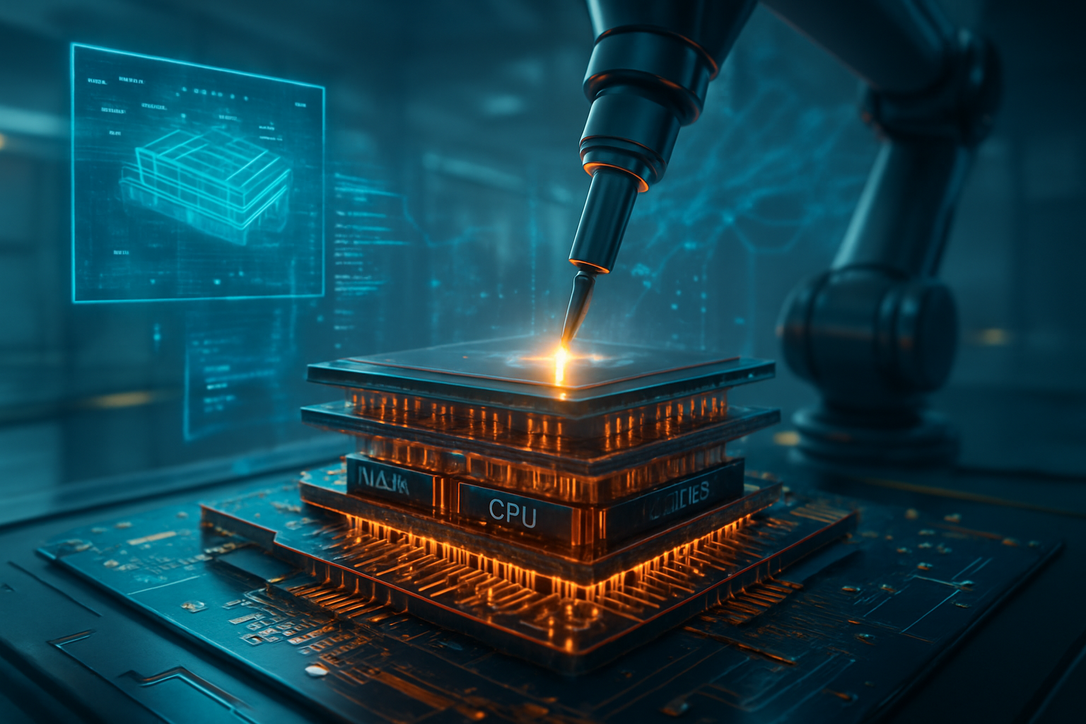
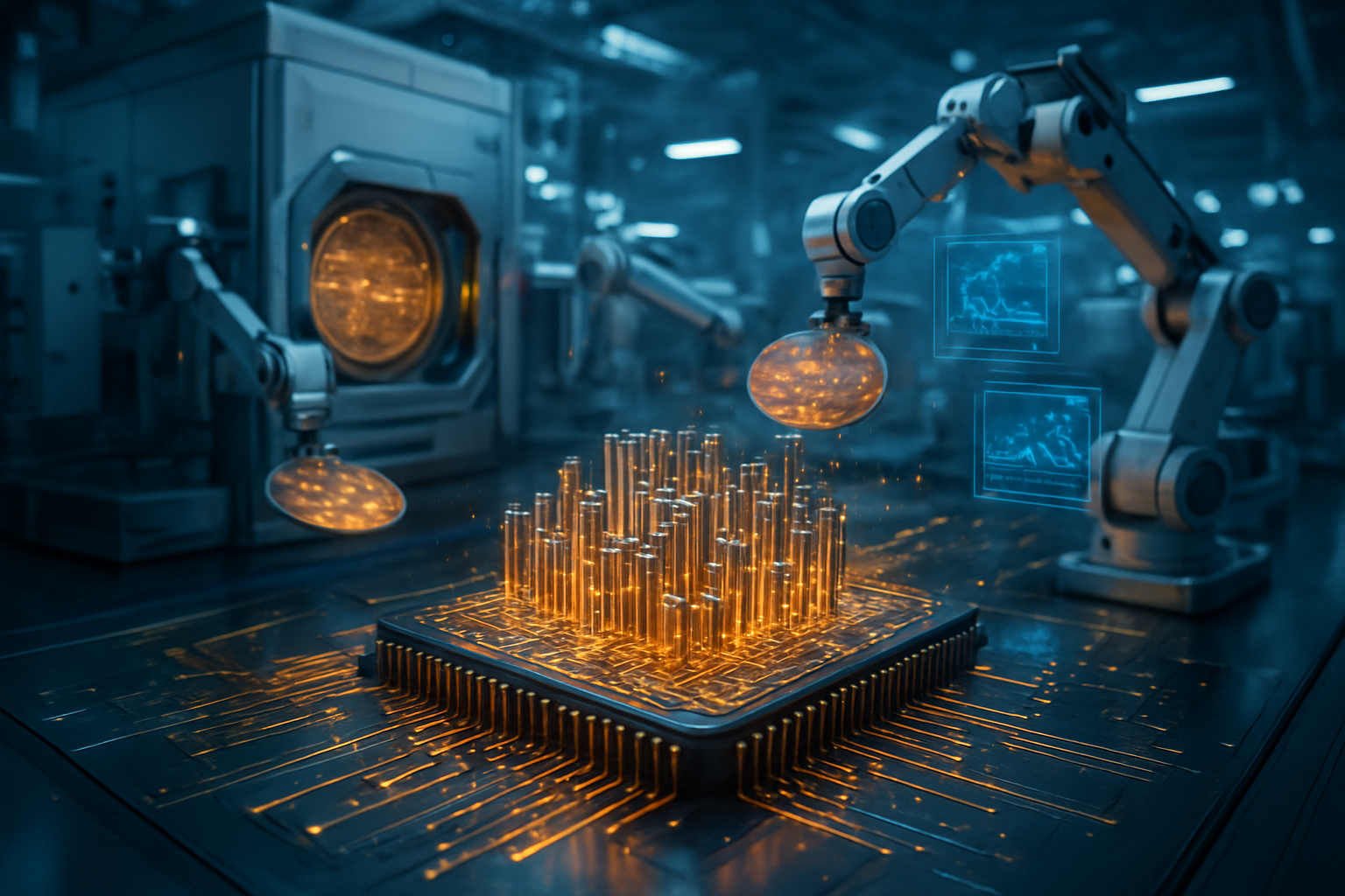
    At the heart of Micron’s fiscal triumph is its industry-leading execution on HBM3E and the rapid prototyping of HBM4. During the earnings call, Micron confirmed it has begun shipping samples of its 12-high HBM4 modules, which feature a groundbreaking bandwidth of 2.8 TB/s and pin speeds of 11 Gbps. This represents a significant leap over current HBM3E standards, utilizing Micron’s proprietary 1-gamma DRAM technology node. Unlike previous generations, which focused primarily on capacity, the HBM4 architecture emphasizes power efficiency—a critical metric for data center operators like NVIDIA (NASDAQ: NVDA) who are struggling to manage the massive thermal envelopes of next-generation AI clusters.

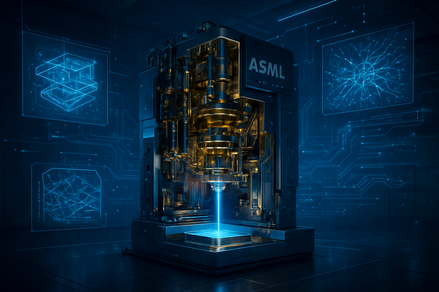
    The technical shift in late 2025 is also marked by the move toward "Custom HBM." Micron revealed a deepened strategic partnership with TSMC (NYSE: TSM) to develop HBM4E modules where the base logic die is co-designed with the customer’s specific AI accelerator. This differs fundamentally from the "one-size-fits-all" approach of the past decade. By integrating the logic die directly into the memory stack using advanced packaging techniques, Micron is reducing latency and power consumption by up to 30% compared to standard configurations. Industry experts have noted that Micron’s yield rates on these complex stacks have now surpassed those of its traditional rivals, positioning the company as a preferred partner for high-performance computing.

    The Competitive Chessboard: Realigning the Semiconductor Sector

    Micron’s blowout quarter has forced a re-evaluation of the competitive landscape among the "Big Three" memory makers. While SK Hynix (KRX: 000660) remains the overall volume leader in HBM, Micron has successfully carved out a premium niche by leveraging its U.S.-based manufacturing footprint and superior power-efficiency ratings. Samsung (KRX: 005930), which struggled with HBM3E yields throughout 2024 and early 2025, is now reportedly in a "catch-up" mode, skipping intermediate nodes to focus on its own 1c DRAM and vertically integrated HBM4 solutions. However, Micron’s "sold out" status through 2026 suggests that Samsung’s recovery may not impact market share until at least 2027.

    For major AI chip designers like AMD (NASDAQ: AMD) and NVIDIA, Micron’s success is a double-edged sword. While it ensures a roadmap for the increasingly powerful memory required for chips like the "Rubin" architecture, the skyrocketing prices of HBM are putting pressure on hardware margins. Startups in the AI hardware space are finding it increasingly difficult to secure memory allocations, as Micron and its peers prioritize long-term agreements with "hyperscalers" and Tier-1 chipmakers. This has created a strategic advantage for established players who can afford to lock in multi-billion-dollar supply contracts years in advance, effectively raising the barrier to entry for new AI silicon challengers.

    A Structural Shift: Beyond the Traditional Commodity Cycle

    The broader significance of this "Memory Supercycle" lies in the decoupling of memory prices from the traditional consumer electronics market. Historically, Micron’s fortunes were tied to the volatile cycles of smartphones and PCs. However, in late 2025, the data center has become the primary driver of DRAM demand. Analysts now view memory as a structural growth industry rather than a cyclical one. A single AI data center deployment now generates demand equivalent to millions of high-end smartphones, creating a "floor" for pricing that was non-existent in previous decades.

    This shift does not come without concerns. The concentration of memory production in the hands of three companies—and the reliance on advanced packaging from a single foundry like TSMC—creates a fragile supply chain. Furthermore, the massive capital expenditure (CapEx) required to stay competitive is eye-watering; Micron has signaled a $20 billion CapEx plan for fiscal 2026. While this fuels innovation, it also risks overcapacity if AI demand were to suddenly plateau. However, compared to previous milestones like the transition to mobile or the cloud, the AI breakthrough appears to have a much longer "runway" due to the fundamental need for massive datasets to reside in high-speed memory for real-time inference.

    The Road to 2028: HBM4E and the $100 Billion Market

    Looking ahead, the trajectory for Micron and the memory sector remains aggressively upward. The company has accelerated its Total Addressable Market (TAM) projections, now expecting the HBM market to reach $100 billion by 2028—two years earlier than previously forecast. Near-term developments will focus on the mass production ramp of HBM4 in mid-2026, which will be essential for the next wave of "sovereign AI" projects where nations build their own localized data centers. We also expect to see the emergence of "Processing-In-Memory" (PIM), where basic computational tasks are handled directly within the DRAM chips to further reduce data movement.

    The challenges remaining are largely physical and economic. As memory stacks grow to 16-high and beyond, the complexity of stacking thin silicon wafers without defects becomes exponential. Experts predict that the industry will eventually move toward "monolithic" 3D DRAM, though that technology is likely several years away. In the meantime, the focus will remain on refining HBM4 and ensuring that the power grid can support the massive energy requirements of these high-performance memory banks.

    Conclusion: A Historic Pivot for Silicon

    Micron’s fiscal Q1 2026 results mark a historic pivot point for the semiconductor industry. By delivering record revenue and margins in the face of immense technical challenges, Micron has proven that memory is the "new oil" of the AI age. The transition from a boom-and-bust commodity cycle to a high-margin, high-growth supercycle is now complete, with Micron standing at the forefront of this transformation. The company’s ability to sell out its 2026 supply a year in advance is perhaps the strongest signal yet that the AI revolution is still in its early, high-growth innings.

    As we look toward the coming months, the industry will be watching for the first production shipments of HBM4 and the potential for Samsung to re-enter the fray as a viable third supplier. For now, however, Micron and SK Hynix hold a formidable duopoly on the high-end memory required for the world's most advanced AI. The "Memory Supercycle" is no longer a forecast—it is the defining economic engine of the late-2025 tech economy.


    This content is intended for informational purposes only and represents analysis of current AI developments.

    TokenRing AI delivers enterprise-grade solutions for multi-agent AI workflow orchestration, AI-powered development tools, and seamless remote collaboration platforms.
    For more information, visit https://www.tokenring.ai/.

  • The Great Silicon Pivot: RISC-V Shatters the Data Center Duopoly as AI Demands Customization

    The Great Silicon Pivot: RISC-V Shatters the Data Center Duopoly as AI Demands Customization

    The landscape of data center architecture has reached a historic turning point. In a move that signals the definitive end of the decades-long x86 and ARM duopoly, Qualcomm (NASDAQ: QCOM) announced this week its acquisition of Ventana Micro Systems, the leading developer of high-performance RISC-V server CPUs. This acquisition, valued at approximately $2.4 billion, represents the largest validation to date of the open-source RISC-V instruction set architecture (ISA) as a primary contender for the future of artificial intelligence and cloud infrastructure.

    The significance of this shift cannot be overstated. As the "Transformer era" of AI places unprecedented demands on power efficiency and memory bandwidth, the rigid licensing models and fixed instruction sets of traditional chipmakers are being bypassed in favor of "silicon sovereignty." By leveraging RISC-V, hyperscalers and chip designers are now able to build domain-specific hardware—tailoring silicon at the gate level to optimize for the specific matrix math and vector processing required by large language models (LLMs).

    The Technical Edge: RVA23 and the Rise of "Custom-Fit" Silicon

    The technical breakthrough propelling RISC-V into the data center is the recent ratification of the RVA23 profile. Previously, RISC-V faced criticism for "fragmentation"—the risk that software written for one RISC-V chip wouldn't run on another. The RVA23 standard, finalized in late 2024, mandates critical features like Hypervisor and Vector extensions, ensuring that standard Linux distributions can run seamlessly across diverse hardware. This standardization, combined with the launch of Ventana’s Veyron V2 platform and Tenstorrent’s Blackhole architecture, has provided the performance parity needed to challenge high-end Xeon and EPYC processors.

    Tenstorrent, led by legendary architect Jim Keller, recently began volume shipments of its Blackhole developer kits. Unlike traditional CPUs that treat AI as an offloaded task, Blackhole integrates RISC-V cores directly with "Tensix" matrix math units on a 6nm process. This architecture offers roughly 2.6 times the performance of its predecessor, Wormhole, by utilizing a 400 Gbps Ethernet-based "on-chip" network that allows thousands of chips to act as a single, unified AI processor. The technical advantage here is "hardware-software co-design": designers can add custom instructions for specific AI kernels, such as sparse tensor operations, which are difficult to implement on the more restrictive ARM (NASDAQ: ARM) or x86 architectures.

    Initial reactions from the research community have been overwhelmingly positive, particularly regarding the flexibility of the RISC-V Vector (RVV) 1.0 extension. Experts note that while ARM's Scalable Vector Extension (SVE) is powerful, RISC-V allows for variable vector lengths that better accommodate the sparse data sets common in modern recommendation engines and generative AI. This level of granularity allows for a 40% to 50% improvement in energy efficiency for inference tasks—a critical metric as data center power consumption becomes a global bottleneck.

    Hyperscale Integration and the Competitive Fallout

    The acquisition of Ventana by Qualcomm is part of a broader trend of vertical integration among tech giants. Meta (NASDAQ: META) has already begun deploying its MTIA 2i (Meta Training and Inference Accelerator) at scale, which utilizes RISC-V cores to handle complex recommendation workloads. In October 2025, Meta further solidified its position by acquiring Rivos, a startup specializing in CUDA-compatible RISC-V designs. This move is a direct shot across the bow of Nvidia (NASDAQ: NVDA), as it aims to bridge the software gap that has long kept developers locked into Nvidia's proprietary ecosystem.

    For incumbents like Intel (NASDAQ: INTC) and AMD (NASDAQ: AMD), the rise of RISC-V represents a fundamental threat to their data center margins. While Intel has joined the RISE (RISC-V Software Ecosystem) project to hedge its bets, the open-source nature of RISC-V allows customers like Google (NASDAQ: GOOGL) and Amazon (NASDAQ: AMZN) to design their own "host" CPUs for their AI accelerators without paying the "x86 tax" or being subject to ARM’s increasingly complex licensing fees. Google has already confirmed it is porting its internal software stack—comprising over 30,000 applications—to RISC-V using AI-powered migration tools.

    The competitive landscape is also shifting toward "sovereign compute." In Europe, the Quintauris consortium—a joint venture between Bosch, Infineon, Nordic, NXP, and Qualcomm—is aggressively funding RISC-V development to reduce the continent's reliance on US-controlled proprietary architectures. This suggests a future where the data center market is no longer dominated by a few central vendors, but rather by a fragmented yet interoperable ecosystem of specialized silicon.

    Geopolitics and the "Linux of Hardware" Moment

    The rise of RISC-V is inextricably linked to the current geopolitical climate. As US export controls continue to restrict the flow of high-end AI chips to China, the open-source nature of RISC-V has provided a lifeline for Chinese tech giants. Alibaba’s (NYSE: BABA) T-Head division recently unveiled the XuanTie C930, a server-grade processor designed to be entirely independent of Western proprietary ISAs. This has turned RISC-V into a "neutral" ground for global innovation, managed by the RISC-V International organization in Switzerland.

    This "neutrality" has led many industry analysts to compare the current moment to the rise of Linux in the 1990s. Just as Linux broke the monopoly of proprietary operating systems by providing a shared, communal foundation, RISC-V is doing the same for hardware. By commoditizing the instruction set, the industry is shifting its focus from "who owns the ISA" to "who can build the best implementation." This democratization of chip design allows startups to compete on merit rather than on the size of their patent portfolios.

    However, this transition is not without concerns. The failure of Esperanto Technologies earlier this year serves as a cautionary tale; despite having a highly efficient 1,000-core RISC-V chip, the company struggled to adapt its architecture to the rapidly evolving "transformer" models that now dominate AI. This highlights the risk of "over-specialization" in a field where the state-of-the-art changes every few months. Furthermore, while the RVA23 profile solves many compatibility issues, the "software moat" built by Nvidia’s CUDA remains a formidable barrier for RISC-V in the high-end training market.

    The Horizon: From Inference to Massive-Scale Training

    In the near term, expect to see RISC-V dominate the AI inference market, particularly for "edge-cloud" applications where power efficiency is paramount. The next major milestone will be the integration of RISC-V into massive-scale AI training clusters. Tenstorrent’s upcoming "Grendel" chip, expected in late 2026, aims to challenge Nvidia's Blackwell successor by utilizing a completely open-source software stack from the compiler down to the firmware.

    The primary challenge remaining is the maturity of the software ecosystem. While projects like RISE are making rapid progress in optimizing compilers like LLVM and GCC for RISC-V, the library support for specialized AI frameworks still lags behind x86. Experts predict that the next 18 months will see a surge in "AI-for-AI" development—using machine learning to automatically optimize RISC-V code, effectively closing the performance gap that previously took decades to bridge via manual tuning.

    A New Era of Compute

    The events of late 2025 have confirmed that RISC-V is no longer a niche curiosity; it is the new standard for the AI era. The Qualcomm-Ventana deal and the mass deployment of RISC-V silicon by Meta and Google signal a move away from "one-size-fits-all" computing toward a future of hyper-optimized, open-source hardware. This shift promises to lower the cost of AI compute, accelerate the pace of innovation, and redistribute the balance of power in the semiconductor industry.

    As we look toward 2026, the industry will be watching the performance of Tenstorrent’s Blackhole clusters and the first fruits of Qualcomm’s integrated RISC-V server designs. The "Great Silicon Pivot" is well underway, and for the first time in the history of the data center, the blueprints for the future are open for everyone to read, modify, and build upon.


    This content is intended for informational purposes only and represents analysis of current AI developments.

    TokenRing AI delivers enterprise-grade solutions for multi-agent AI workflow orchestration, AI-powered development tools, and seamless remote collaboration platforms.
    For more information, visit https://www.tokenring.ai/.

  • The Goldilocks Rally: How Cooling Inflation and the ‘Sovereign AI’ Boom Pushed Semiconductors to All-Time Highs

    The Goldilocks Rally: How Cooling Inflation and the ‘Sovereign AI’ Boom Pushed Semiconductors to All-Time Highs

    As 2025 draws to a close, the global financial markets are witnessing a historic convergence of macroeconomic stability and relentless technological expansion. On December 18, 2025, the semiconductor sector solidified its position as the undisputed engine of the global economy, with the PHLX Semiconductor Sector (SOX) Index hovering near its recent all-time high of 7,490.28. This massive rally, which has seen chip stocks surge by over 35% year-to-date, is being fueled by a "perfect storm": a decisive cooling of inflation that has allowed the Federal Reserve to pivot toward aggressive interest rate cuts, and a second wave of artificial intelligence (AI) investment known as "Sovereign AI."

    The significance of this moment cannot be overstated. For the past two years, the tech sector has grappled with the dual pressures of high borrowing costs and "AI skepticism." However, the November Consumer Price Index (CPI) report, which showed inflation dropping to a surprising 2.7%—well below the 3.1% forecast—has effectively silenced the bears. With the Federal Open Market Committee (FOMC) delivering its third consecutive 25-basis-point rate cut on December 10, the cost of capital for massive AI infrastructure projects has plummeted just as the industry transitions from the "training phase" to the even more compute-intensive "inference phase."

    The Rise of the 'Rubin' Era and the 3nm Transition

    The technical backbone of this rally lies in the rapid acceleration of the semiconductor roadmap, specifically the transition to 3nm process nodes and the introduction of next-generation architectures. NVIDIA (NASDAQ: NVDA) has dominated headlines with the formal preview of its "Vera Rubin" architecture, the successor to the highly successful Blackwell platform. Built on TSMC (NYSE: TSM) N3P (3nm) process, the Vera Rubin R100 GPU represents a paradigm shift from individual accelerators to "AI Factories." By utilizing advanced CoWoS-L packaging, NVIDIA has achieved a 4x reticle design, allowing for a staggering 50 PFLOPS of FP4 precision—roughly 2.5 times the performance of the Blackwell B200.

    While NVIDIA remains the leader, AMD (NASDAQ: AMD) has successfully carved out a massive share of the AI inference market with its Instinct MI350 series. Launched in late 2025, the MI350 is built on the CDNA 4 architecture and features 288GB of HBM3e memory. AMD’s strategic integration of ZT Systems has allowed the company to offer full-stack AI rack solutions that compete directly with NVIDIA’s GB200 NVL72 systems. Industry experts note that the MI350’s 35x improvement in inference efficiency over the previous generation has made it the preferred choice for hyperscalers like Meta (NASDAQ: META) and Microsoft (NASDAQ: MSFT), who are increasingly focused on the operational costs of running live AI models.

    The "bottleneck breaker" of late 2025, however, is High Bandwidth Memory 4 (HBM4). As GPU logic speeds have outpaced data delivery, the "Memory Wall" became a critical concern for AI developers. The shift to HBM4, led by SK Hynix (KRX: 000660) and Micron (NASDAQ: MU), has doubled the interface width to 2048-bit, providing up to 13.5 TB/s of bandwidth. This breakthrough allows a single GPU to hold trillion-parameter models in local memory, drastically reducing the latency and energy consumption associated with data transfer. Micron’s blowout earnings report on December 17, which sent the stock up 15%, served as a validation of this trend, proving that the AI rally is no longer just about the chips, but the entire memory and networking ecosystem.

    Hyperscalers and the New Competitive Landscape

    The cooling inflation environment has acted as a green light for "Big Tech" to accelerate their capital expenditure (Capex). Major players like Amazon (NASDAQ: AMZN) and Google (NASDAQ: GOOGL) have signaled that their 2026 budgets will prioritize AI infrastructure over almost all other initiatives. This has created a massive backlog for foundries like TSMC, which is currently operating at 100% capacity for its advanced CoWoS packaging. The strategic advantage has shifted toward companies that can secure guaranteed supply; consequently, long-term supply agreements have become the most valuable currency in Silicon Valley.

    For the major AI labs and tech giants, the competitive implications are profound. The ability to deploy "Vera Rubin" clusters at scale in 2026 will likely determine the leaders of the next generation of Large Language Models (LLMs). Companies that hesitated during the high-interest-rate environment of 2023-2024 are now finding themselves at a significant disadvantage, as the "compute divide" between the haves and the have-nots continues to widen. Startups, meanwhile, are pivoting toward "Edge AI" and specialized inference chips to avoid competing directly with the trillion-dollar hyperscalers for data center space.

    The market positioning of ASML (NASDAQ: ASML) and ARM (NASDAQ: ARM) has also strengthened. As the industry moves toward 2nm production in late 2025, ASML’s High-NA EUV lithography machines have become indispensable. Similarly, ARM’s custom "Vera CPU" and its integration into NVIDIA’s Grace-Rubin superchips have cemented the Arm architecture as the standard for AI orchestration, challenging the traditional dominance of x86 processors in the data center.

    Sovereign AI: The Geopolitical Catalyst

    Beyond the corporate sector, the late 2025 rally is being propelled by the "Sovereign AI" movement. Nations are now treating compute capacity as a critical national resource, similar to energy or food security. This trend has moved from theory to massive capital deployment. Saudi Arabia’s HUMAIN Project, a $77 billion initiative, has already secured tens of thousands of Blackwell and Rubin chips to build domestic AI clusters powered by the Kingdom's vast solar resources. Similarly, the UAE’s "Stargate" cluster, built in partnership with Microsoft and OpenAI, aims to reach 5GW of capacity by the end of the decade.

    This shift represents a fundamental change in the AI landscape. Unlike the early days of the AI boom, which were driven by a handful of US-based tech companies, the current phase is global. France has committed €10 billion to build a decarbonized supercomputer powered by nuclear energy, while India’s IndiaAI Mission is deploying over 50,000 GPUs to support indigenous model training. This "National Compute" trend provides a massive, non-cyclical floor for semiconductor demand, as government budgets are less sensitive to the short-term market fluctuations that typically affect the tech sector.

    However, this global race for AI supremacy has raised concerns regarding energy consumption and "compute nationalism." The massive power requirements of these national clusters—some reaching 1GW or more—are straining local power grids and forcing a rapid acceleration of modular nuclear reactor (SMR) technology. Furthermore, as countries build their own "walled gardens" of AI infrastructure, the dream of a unified, global AI ecosystem is being replaced by a fragmented landscape of culturally and politically aligned models.

    The Road to 2nm and Beyond

    Looking ahead, the semiconductor sector shows no signs of slowing down. The most anticipated development for 2026 is the transition to mass production of 2nm chips. TSMC has already begun accepting orders for its 2nm process, with Apple (NASDAQ: AAPL) and NVIDIA expected to be the first in line. This transition will introduce "GAAFET" (Gate-All-Around Field-Effect Transistor) technology, offering a 15% speed improvement and a 30% reduction in power consumption compared to the 3nm node.

    In the near term, the industry will focus on the deployment of HBM4-equipped GPUs and the integration of "Liquid-to-Air" cooling systems in data centers. As power densities per rack exceed 100kW, traditional air cooling is no longer viable, leading to a boom for specialized thermal management companies. Experts predict that the next frontier will be "Optical Interconnects," which use light instead of electricity to move data between chips, potentially solving the final bottleneck in AI scaling.

    The primary challenge remains the geopolitical tension surrounding the semiconductor supply chain. While the "Goldilocks" macro environment has eased financial pressures, the concentration of advanced manufacturing in East Asia remains a systemic risk. Efforts to diversify production to the United States and Europe through the CHIPS Act are progressing, but it will take several more years before these regions can match the scale and efficiency of the existing Asian ecosystem.

    A Historic Milestone for the Silicon Economy

    The semiconductor rally of late 2025 marks a definitive turning point in economic history. It is the moment when "Silicon" officially replaced "Oil" as the world's most vital commodity. The combination of cooling inflation and the explosion of Sovereign AI has created a structural demand for compute that is decoupled from traditional business cycles. For investors, the takeaway is clear: semiconductors are no longer a cyclical "tech play," but the fundamental infrastructure of the 21st-century economy.

    As we move into 2026, the industry's focus will shift from "how many chips can we build?" to "how much power can we find?" The energy constraints of AI factories will likely be the defining narrative of the coming year. For now, however, the "Santa Claus Rally" in chip stocks provides a festive end to a year of extraordinary growth. Investors should keep a close eye on the first batch of 2nm test results from TSMC and the official launch of the Vera Rubin platform in early 2026, as these will be the next major catalysts for the sector.


    This content is intended for informational purposes only and represents analysis of current AI developments.

    TokenRing AI delivers enterprise-grade solutions for multi-agent AI workflow orchestration, AI-powered development tools, and seamless remote collaboration platforms.
    For more information, visit https://www.tokenring.ai/.


    Note: Public companies mentioned include NVIDIA (NASDAQ: NVDA), AMD (NASDAQ: AMD), TSMC (NYSE: TSM), Micron (NASDAQ: MU), ASML (NASDAQ: ASML), ARM (NASDAQ: ARM), Microsoft (NASDAQ: MSFT), Amazon (NASDAQ: AMZN), Meta (NASDAQ: META), Apple (NASDAQ: AAPL), Alphabet/Google (NASDAQ: GOOGL), Samsung (KRX: 005930), and SK Hynix (KRX: 000660).

  • The 1.6T Breakthrough: How MACOM’s Analog Innovations are Powering the 100,000-GPU AI Era

    The 1.6T Breakthrough: How MACOM’s Analog Innovations are Powering the 100,000-GPU AI Era

    As of December 18, 2025, the global race for artificial intelligence supremacy has moved beyond the chip itself and into the very fabric that connects them. With Tier-1 AI labs now deploying "Gigawatt-scale" AI factories featuring upwards of 100,000 GPUs, the industry has hit a critical bottleneck: the "networking wall." To shatter this barrier, MACOM Technology Solutions (NASDAQ: MTSI) has emerged as a linchpin of the modern data center, providing the high-performance analog and mixed-signal semiconductors essential for the transition to 800G and 1.6 Terabit (1.6T) data throughput.

    The immediate significance of MACOM’s recent advancements cannot be overstated. In a year defined by the massive ramp-up of the NVIDIA (NASDAQ: NVDA) Blackwell architecture and the emergence of 200,000-GPU clusters like xAI’s Colossus, the demand for "east-west" traffic—the communication between GPUs—has reached a staggering 80 Petabits per second in some facilities. MACOM’s role in enabling 200G-per-lane connectivity and its pioneering "DSP-free" optical architectures have allowed hyperscalers to scale these clusters while slashing power consumption and latency, two factors that previously threatened to stall the progress of frontier AI models.

    The Technical Frontier: 200G Lanes and the Death of the DSP

    At the heart of MACOM’s 2025 success is the shift to 200G-per-lane technology. While 400G and early 800G networks relied on 100G lanes, the 1.6T era requires doubling that density. MACOM’s recently launched chipset portfolio for 1.6T connectivity includes Transimpedance Amplifiers (TIAs) and laser drivers capable of 212 Gbps per lane. This technical leap is facilitated by MACOM’s proprietary Indium Phosphide (InP) process, which allows for the high-sensitivity photodetectors and high-power Continuous Wave (CW) lasers necessary to maintain signal integrity at these extreme frequencies.

    One of the most disruptive technologies in MACOM’s arsenal is its PURE DRIVE™ Linear Pluggable Optics (LPO) ecosystem. Traditionally, optical modules use a Digital Signal Processor (DSP) to "clean up" the signal, but this adds significant power draw and roughly 200 nanoseconds of latency. In the world of synchronous AI training, where thousands of GPUs must wait for the slowest signal to arrive, 200 nanoseconds is an eternity. MACOM’s LPO solutions remove the DSP entirely, relying on high-performance analog components to maintain signal quality. This reduces module power consumption by up to 50% and slashes latency to under 5 nanoseconds, a feat that has drawn widespread praise from the AI research community for its ability to maximize "GPU utilization" rates.

    Furthermore, MACOM has addressed the physical constraints of the data center with its Active Copper Cable (ACC) solutions. As AI racks become more densely packed, the heat generated by traditional optics becomes unmanageable. MACOM’s linear equalizers allow copper cables to reach distances of up to 2.5 meters at 226 Gbps speeds. This allows for "in-rack" 1.6T connections to remain on copper, which is not only cheaper but also significantly more energy-efficient than optical alternatives, providing a critical "thermal relief valve" for high-density GPU clusters.

    Market Dynamics: The Beneficiaries of the Analog Renaissance

    The strategic positioning of MACOM (NASDAQ: MTSI) has made it a primary beneficiary of the massive CAPEX spending by hyperscalers like Meta (NASDAQ: META), Microsoft (NASDAQ: MSFT), and Google (NASDAQ: GOOGL). As these giants transition their backbones from 400G to 800G and 1.6T, they are increasingly looking for ways to bypass the high costs and power requirements of traditional retimed (DSP-based) modules. MACOM’s architecture-agnostic approach—supporting both retimed and linear configurations—allows it to capture market share regardless of which specific networking standard a hyperscaler adopts.

    In the competitive landscape, MACOM is carving out a unique niche against larger rivals like Broadcom (NASDAQ: AVGO) and Marvell Technology (NASDAQ: MRVL). While Broadcom dominates the switch ASIC market with its Tomahawk 6 series, MACOM provides the essential "front-end" analog components that interface with those switches. The partnership between MACOM’s analog expertise and the latest 102.4 Tbps switch chips has created a formidable ecosystem that is difficult for startups to penetrate. For AI labs, the strategic advantage of using MACOM-powered LPO modules lies in the "Total Cost of Ownership" (TCO); by reducing power by several watts per port across a 100,000-port cluster, a data center operator can save millions in annual electricity and cooling costs.

    Wider Significance: Enabling the Gigawatt-Scale AI Factory

    The rise of MACOM’s technology fits into a broader trend of "Scale-Across" architectures. In 2025, a single data center building often cannot support the 300MW to 500MW required for a 200,000-GPU cluster. This has led to the creation of virtual clusters spread across multiple buildings within a campus. MACOM’s high-performance optics are the "connective tissue" that enables these buildings to communicate with the ultra-low latency required to function as a single unit. Without the signal integrity provided by high-performance analog semiconductors, the latency introduced by distance would cause the entire AI training process to desynchronize.

    However, the rapid scaling of these facilities has also raised concerns. The environmental impact of "Gigawatt-scale" sites is under intense scrutiny. MACOM’s focus on power efficiency via DSP-free optics is not just a technical preference but a necessity for the industry’s survival in a world of limited power grids. Comparing this to previous milestones, the jump from 100G to 1.6T in just a few years represents a faster acceleration of networking bandwidth than at any other point in the history of the internet, driven entirely by the insatiable data appetite of Large Language Models (LLMs).

    Future Outlook: The Road to 3.2T and Beyond

    Looking ahead to 2026, the industry is already eyeing the 3.2 Terabit (3.2T) horizon. At the 2025 Optical Fiber Conference, MACOM showcased preliminary 3.2T transmit solutions utilizing 400G-per-lane data rates. While 1.6T is currently the "bleeding edge," the roadmap suggests that the 400G-per-lane transition will be the next major battleground. To meet these demands, experts predict a shift toward Co-Packaged Optics (CPO), where the optical engine is moved directly onto the switch substrate to further reduce power. MACOM’s expertise in chip-stacked TIAs and photodetectors positions them perfectly for this transition.

    The near-term challenge remains the manufacturing yield of 200G-per-lane components. As frequencies increase, the margin for error in semiconductor fabrication shrinks. However, MACOM’s recent award of CHIPS Act funding for GaN-on-SiC and other advanced materials suggests that they have the federal backing to continue innovating in high-speed RF and power applications. Analysts expect MACOM to reach a $1 billion annual revenue run rate by fiscal 2026, fueled by the continued "multi-year growth cycle" of AI infrastructure.

    Conclusion: The Analog Foundation of Digital Intelligence

    In summary, MACOM Technology Solutions has proven that in an increasingly digital world, the most critical innovations are often analog. By enabling the 1.6T networking cycle and providing the components that make 100,000-GPU clusters viable, MACOM has cemented its place as a foundational player in the AI era. Their success in 2025 highlights a shift in the industry's focus from pure compute power to the efficiency and speed of data movement.

    As we look toward the coming months, watch for the first mass-scale deployments of 1.6T LPO modules in "Blackwell-Ultra" clusters. The ability of these systems to maintain high utilization rates will be the ultimate test of MACOM’s technology. In the history of AI, the transition to 1.6T will likely be remembered as the moment the "networking wall" was finally dismantled, allowing for the training of models with trillions of parameters that were previously thought to be computationally—and logistically—impossible.


    This content is intended for informational purposes only and represents analysis of current AI developments.

    TokenRing AI delivers enterprise-grade solutions for multi-agent AI workflow orchestration, AI-powered development tools, and seamless remote collaboration platforms.
    For more information, visit https://www.tokenring.ai/.

  • The Invisible Backbone of AI: Why Advanced Packaging is the New Battleground for Semiconductor Dominance

    The Invisible Backbone of AI: Why Advanced Packaging is the New Battleground for Semiconductor Dominance

    As the artificial intelligence revolution accelerates into late 2025, the industry’s focus has shifted from the raw transistor counts of chips to the sophisticated architecture that holds them together. While massive Large Language Models (LLMs) continue to demand unprecedented compute power, the primary bottleneck is no longer just the speed of the processor, but the "memory wall"—the physical limit of how fast data can travel between memory and logic. Advanced packaging has emerged as the critical solution to this crisis, transforming from a secondary manufacturing step into the primary frontier of semiconductor innovation.

    At the heart of this transition is Kulicke and Soffa Industries (NASDAQ: KLIC), a company that has successfully pivoted from its legacy as a leader in traditional wire bonding to becoming a pivotal player in the high-stakes world of AI advanced packaging. By enabling the complex stacking and interconnectivity required for High Bandwidth Memory (HBM) and chiplet architectures, KLIC is proving that the future of AI performance will be won not just by the designers of chips, but by the masters of assembly.

    The Technical Leap: Solving the Memory Wall with Fluxless TCB

    The technical challenge of 2025 AI hardware lies in the transition from 2D layouts to 2.5D and 3D heterogeneous architectures. Traditional wire bonding, which uses thin gold or copper wires to connect chips to their packages, is increasingly insufficient for the ultra-high-speed requirements of AI GPUs like the Blackwell series from NVIDIA (NASDAQ: NVDA). These modern accelerators require thousands of microscopic connections, known as micro-bumps, to be placed with sub-10-micron precision. This is where KLIC’s Advanced Solutions segment, specifically its APTURA™ series, has become indispensable.

    KLIC’s breakthrough technology is Fluxless Thermo-Compression Bonding (FTC). Unlike traditional methods that use chemical flux to remove oxidation—a process that leaves behind residues difficult to clean at the fine pitches required for HBM4—KLIC’s FTC uses a formic acid vapor in-situ. This "dry" process ensures a cleaner, more reliable bond, allowing for an interconnect pitch as small as 8 micrometers. This level of precision is vital for the 12- and 16-layer HBM stacks that provide the 4TB/s+ bandwidth necessary for next-generation AI training.

    Furthermore, KLIC has introduced the CuFirst™ Hybrid Bonding technology. While traditional bonding relies on heat and pressure to melt solder bumps, hybrid bonding allows copper-to-copper interconnects at room temperature, followed by a dielectric seal. This "bumpless" approach significantly reduces the distance data must travel, cutting latency and reducing power consumption by up to 40% compared to previous generations. By providing these tools, KLIC is enabling the industry to move beyond the physical limits of traditional silicon scaling, a trend often referred to as "More than Moore."

    Market Impact: Navigating the CoWoS Supply Chain

    The strategic importance of advanced packaging is best reflected in the supply chain of Taiwan Semiconductor Manufacturing Company (NYSE: TSM), the world’s leading foundry. In late 2025, TSMC’s Chip-on-Wafer-on-Substrate (CoWoS) capacity has become the most valuable real estate in the tech world. As TSMC doubled its CoWoS capacity to roughly 80,000 wafers per month to meet the demands of NVIDIA and Advanced Micro Devices (NASDAQ: AMD), the equipment providers that qualify for these lines have seen their market positions solidify.

    KLIC has successfully broken into this elite circle, qualifying its fluxless TCB systems for TSMC’s CoWoS-L process. This has placed KLIC in direct competition with incumbents like ASMPT (HKG: 0522) and BE Semiconductor Industries (AMS: BESI). While ASMPT remains a high-volume leader in the broader market, KLIC’s specialized focus on fluxless technology has made it a preferred partner for the high-yield, high-reliability requirements of AI server modules. For companies like NVIDIA, having multiple qualified equipment vendors like KLIC ensures a more resilient supply chain and helps mitigate the chronic shortages that plagued the industry in 2023 and 2024.

    The shift also benefits AMD, which has been more aggressive in adopting 3D chiplet architectures. AMD’s MI350 series, launched earlier this year, utilizes 3D hybrid bonding to stack compute chiplets directly onto I/O dies. This architectural choice gives AMD a competitive edge in power efficiency, a metric that has become as important as raw speed for data center operators. As these tech giants battle for AI supremacy, their reliance on advanced packaging equipment providers has effectively turned companies like KLIC into the "arms dealers" of the AI era.

    The Wider Significance: Beyond Moore's Law

    The rise of advanced packaging marks a fundamental shift in the semiconductor landscape. For decades, the industry followed Moore’s Law, doubling transistor density every two years by shrinking the size of individual transistors. However, as transistors approach the atomic scale, the cost and complexity of further shrinking have skyrocketed. Advanced packaging offers a way out of this economic trap by allowing engineers to "disaggregate" the chip into smaller, specialized chiplets that can be manufactured on different process nodes and then stitched together.

    This trend has profound geopolitical implications. Under the U.S. CHIPS Act and similar initiatives in Europe and Japan, there is a renewed focus on bringing packaging capabilities back to Western shores. Historically, packaging was seen as a low-margin, labor-intensive "back-end" process that was outsourced to Southeast Asia. In 2025, it is recognized as a high-tech, high-margin "mid-end" process essential for national security and technological sovereignty. KLIC, as a U.S.-headquartered company with a deep global footprint, is uniquely positioned to benefit from this reshoring trend.

    Furthermore, the environmental impact of AI is under intense scrutiny. The energy required to move data between a processor and its memory can often exceed the energy used for the actual computation. By using KLIC’s advanced bonding technologies to place memory closer to the logic, the industry is making significant strides in "Green AI." Reducing the parasitic capacitance of interconnects is no longer just a technical goal; it is a sustainability mandate for the world's largest data center operators.

    Future Outlook: The Road to Glass Substrates and CPO

    Looking toward 2026 and 2027, the roadmap for advanced packaging includes even more radical shifts. One of the most anticipated developments is the move from organic substrates to glass substrates. Glass offers superior flatness and thermal stability, which will be necessary as AI chips grow larger and hotter. Companies like KLIC are already in R&D phases for equipment that can handle the unique handling and bonding requirements of glass, which is far more brittle than the materials used today.

    Another major horizon is Co-Packaged Optics (CPO). As electrical signals struggle to maintain integrity over longer distances, the industry is looking to integrate optical fibers directly into the chip package. This would allow data to be transmitted via light rather than electricity, virtually eliminating the "memory wall" and enabling massive clusters of GPUs to act as a single, giant processor. The precision required to align these optical fibers is an order of magnitude higher than even today’s most advanced TCB, representing the next great challenge for KLIC’s engineering teams.

    Experts predict that by 2027, the "Year of HBM4," hybrid bonding will move from niche applications into high-volume manufacturing. While TCB remains the workhorse for today's Blackwell and MI350 chips, the transition to hybrid bonding will require a massive new cycle of capital expenditure. The winners will be those who can provide high-throughput machines that maintain sub-micron accuracy in a high-volume factory environment.

    A New Era of Semiconductor Assembly

    The transformation of Kulicke and Soffa from a wire-bonding specialist into an advanced packaging powerhouse is a microcosm of the broader shift in the semiconductor industry. As AI models grow in complexity, the "package" has become as vital as the "chip." The ability to stack, connect, and cool these massive silicon systems is now the primary determinant of who leads the AI race.

    Key takeaways from this development include the critical role of fluxless bonding in improving yields for HBM4 and the strategic importance of being qualified in the TSMC CoWoS supply chain. As we move further into 2026, the industry will be watching for the first high-volume applications of glass substrates and the continued adoption of hybrid bonding.

    For investors and industry observers, the message is clear: the next decade of AI breakthroughs will not just be written in code or silicon, but in the microscopic copper interconnects that bind them together. Advanced packaging is no longer the final step in the process; it is the foundation upon which the future of artificial intelligence is being built.


    This content is intended for informational purposes only and represents analysis of current AI developments.

    TokenRing AI delivers enterprise-grade solutions for multi-agent AI workflow orchestration, AI-powered development tools, and seamless remote collaboration platforms.
    For more information, visit https://www.tokenring.ai/.

  • The High-NA Frontier: ASML Solidifies the Sub-2nm Era as EUV Adoption Hits Critical Mass

    The High-NA Frontier: ASML Solidifies the Sub-2nm Era as EUV Adoption Hits Critical Mass

    As of late 2025, the semiconductor industry has reached a historic inflection point, driven by the successful transition of High-Numerical Aperture (High-NA) Extreme Ultraviolet (EUV) lithography from experimental labs to the factory floor. ASML (NASDAQ: ASML), the world’s sole provider of the machinery required to print the world’s most advanced chips, has officially entered the high-volume manufacturing (HVM) phase for its next-generation systems. This milestone marks the beginning of the sub-2nm era, providing the essential infrastructure for the next decade of artificial intelligence, high-performance computing, and mobile technology.

    The immediate significance of this development cannot be overstated. With the shipment of the Twinscan EXE:5200B to major foundries, the industry has solved the "stitching" and throughput challenges that once threatened to stall Moore’s Law. For ASML, the successful ramp of these multi-hundred-million-dollar machines is the primary engine behind its projected 2030 revenue targets of up to €60 billion. As logic and DRAM manufacturers race to integrate these tools, the gap between those who can afford the "bleeding edge" and those who cannot has never been wider.

    Breaking the Sub-2nm Barrier: The Technical Triumph of High-NA

    The technical centerpiece of ASML’s 2025 success is the EXE:5200B, a machine that represents the pinnacle of human engineering. Unlike standard EUV tools, which use a 0.33 Numerical Aperture (NA) lens, High-NA systems utilize a 0.55 NA anamorphic lens system. This allows for a significantly higher resolution, enabling chipmakers to print features as small as 8nm—a requirement for the 1.4nm (A14) and 1nm nodes. By late 2025, ASML has successfully boosted the throughput of these systems to 175–200 wafers per hour (wph), matching the productivity of previous generations while drastically reducing the need for "multi-patterning."

    One of the most significant technical hurdles overcome this year was "reticle stitching." Because High-NA lenses are anamorphic (magnifying differently in the X and Y directions), the field size is halved compared to standard EUV. This required engineers to "stitch" two halves of a chip design together with nanometer precision. Reports from IMEC and Intel (NASDAQ: INTC) in mid-2025 confirmed that this process has stabilized, allowing for the production of massive AI accelerators that exceed traditional size limits. Furthermore, the industry has begun transitioning to Metal Oxide Resists (MOR), which are thinner and more sensitive than traditional chemically amplified resists, allowing the High-NA light to be captured more effectively.

    Initial reactions from the research community have been overwhelmingly positive, with experts noting that High-NA reduces the number of process steps by over 40 on critical layers. This reduction in complexity is vital for yield management at the 1.4nm node. While the sheer cost of the machines—estimated at over $380 million each—initially caused hesitation, the data from 2025 pilot lines has proven that the reduction in mask sets and processing time makes High-NA a cost-effective solution for the highest-volume, highest-performance chips.

    The Foundry Arms Race: Intel, TSMC, and Samsung Diverge

    The adoption of High-NA has created a strategic divide among the "Big Three" chipmakers. Intel has emerged as the most aggressive pioneer, having fully installed two production-grade EXE:5200 units at its Oregon facility by late 2025. Intel is betting its entire "Intel 14A" roadmap on being the first to market with High-NA, aiming to reclaim the crown of process leadership from TSMC (NYSE: TSM). For Intel, the strategic advantage lies in early mastery of the tool’s quirks, potentially allowing them to offer 1.4nm capacity to external foundry customers before their rivals.

    TSMC, conversely, has maintained a pragmatic stance for much of 2025, focusing on its N2 and A16 nodes using standard EUV with multi-patterning. However, the tide shifted in late 2025 when reports surfaced that TSMC had placed significant orders for High-NA machines to support its A14P node, expected to ramp in 2027-2028. This move signals that even the most cost-conscious foundry leader recognizes that standard EUV cannot scale indefinitely. Samsung (KRX: 005930) also took delivery of its first production High-NA unit in Q4 2025, intending to use the technology for its SF1.4 node to close the performance gap in the mobile and AI markets.

    The implications for the broader market are profound. Companies like NVIDIA (NASDAQ: NVDA) and Apple (NASDAQ: AAPL) are now forced to navigate this fragmented landscape, deciding whether to stick with TSMC’s proven 0.33 NA methods or pivot to Intel’s High-NA-first approach for their next-generation AI GPUs and silicon. This competition is driving a "supercycle" for ASML, as every major player is forced to buy the most expensive equipment just to stay in the race, further cementing ASML’s monopoly at the top of the supply chain.

    Beyond Logic: EUV’s Critical Role in DRAM and Global Trends

    While logic manufacturing often grabs the headlines, 2025 has been the year EUV became indispensable for memory. The mass production of "1c" (12nm-class) DRAM is now in full swing, with SK Hynix (KRX: 000660) leading the charge by utilizing five to six EUV layers for its HBM4 (High Bandwidth Memory) products. Even Micron (NASDAQ: MU), which was famously the last major holdout for EUV technology, has successfully ramped its 1-gamma node using EUV at its Hiroshima plant this year. The integration of EUV in DRAM is critical for ASML’s long-term margins, as memory manufacturers typically purchase tools in higher volumes than logic foundries.

    This shift fits into a broader global trend: the AI Supercycle. The explosion in demand for generative AI has created a bottomless appetite for high-density memory and high-performance logic, both of which now require EUV. However, this growth is occurring against a backdrop of geopolitical complexity. ASML has reported that while demand from China has normalized—dropping to roughly 20% of revenue from nearly 50% in 2024 due to export restrictions—the global demand for advanced tools has more than compensated. ASML’s gross margin targets of 56% to 60% by 2030 are predicated on this shift toward higher-value High-NA systems and the expansion of EUV into the memory sector.

    Comparisons to previous milestones, such as the initial move from DUV to EUV in 2018, suggest that we are entering a "harvesting" phase. The foundational science is settled, and the focus has shifted to industrialization and yield optimization. The potential concern remains the "cost wall"—the risk that only a handful of companies can afford to design chips at the 1.4nm level, potentially centralizing the AI industry even further into the hands of a few tech giants.

    The Roadmap to 2030: From High-NA to Hyper-NA

    Looking ahead, ASML is already laying the groundwork for the next decade with "Hyper-NA" lithography. As High-NA carries the industry through the 1.4nm and 1nm eras, the subsequent generation of transistors—likely based on Complementary FET (CFET) architectures—will require even higher resolution. ASML’s roadmap for the HXE series targets a 0.75 NA, which would be the most significant jump in optical capability in the company's history. Pilot systems for Hyper-NA are currently projected for introduction around 2030.

    The challenges for Hyper-NA are daunting. At 0.75 NA, the depth of focus becomes extremely shallow, and light polarization effects can degrade image contrast. ASML is currently researching specialized polarization filters and even more advanced photoresist materials to combat these physics-based limitations. Experts predict that the move to Hyper-NA will be as difficult as the original transition to EUV, requiring a complete overhaul of the mask and pellicle ecosystem. However, if successful, it will extend the life of silicon-based computing well into the 2030s.

    In the near term, the industry will focus on the "A14" ramp. We expect to see the first silicon samples from Intel’s High-NA lines by mid-2026, which will be the ultimate test of whether the technology can deliver on its promise of superior power, performance, and area (PPA). If Intel succeeds in hitting its yield targets, it could trigger a massive wave of "FOMO" (fear of missing out) among other chipmakers, leading to an even faster adoption rate for ASML’s most advanced tools.

    Conclusion: The Indispensable Backbone of AI

    The status of ASML and EUV lithography at the end of 2025 confirms one undeniable truth: the future of artificial intelligence is physically etched by a single company in Veldhoven. The successful deployment of High-NA lithography has effectively moved the goalposts for Moore’s Law, ensuring that the roadmap to sub-2nm chips is not just a theoretical possibility but a manufacturing reality. ASML’s ability to maintain its technological lead while expanding its margins through logic and DRAM adoption has solidified its position as the most critical node in the global technology supply chain.

    As we move into 2026, the industry will be watching for the first "High-NA chips" to enter the market. The success of these products will determine the pace of the next decade of computing. For now, ASML has proven that it can meet the moment, providing the tools necessary to build the increasingly complex brains of the AI era. The "High-NA Era" has officially arrived, and with it, a new chapter in the history of human innovation.


    This content is intended for informational purposes only and represents analysis of current AI developments.

    TokenRing AI delivers enterprise-grade solutions for multi-agent AI workflow orchestration, AI-powered development tools, and seamless remote collaboration platforms.
    For more information, visit https://www.tokenring.ai/.

  • The Silicon Bedrock: Strengthening Forecasts for AI Chip Equipment Signal a Multi-Year Infrastructure Supercycle

    The Silicon Bedrock: Strengthening Forecasts for AI Chip Equipment Signal a Multi-Year Infrastructure Supercycle

    As 2025 draws to a close, the semiconductor industry is witnessing a historic shift in capital allocation, driven by a "giga-cycle" of investment in artificial intelligence infrastructure. According to the latest year-end reports from industry authority SEMI and leading equipment manufacturers, global Wafer Fab Equipment (WFE) spending is forecast to hit a record-breaking $145 billion in 2026. This surge is underpinned by an insatiable demand for next-generation AI processors and high-bandwidth memory, forcing a radical retooling of the world’s most advanced fabrication facilities.

    The immediate significance of this development cannot be overstated. We are moving past the era of "AI experimentation" into a phase of "AI industrialization," where the physical limits of silicon are being pushed by revolutionary new architectures. Leaders in the space, most notably Applied Materials (NASDAQ: AMAT), have reported record annual revenues of over $28 billion for fiscal 2025, with visibility into customer factory plans extending well into 2027. This strengthening forecast suggests that the "pick and shovel" providers of the AI gold rush are entering their most profitable era yet, as the industry races toward a $1 trillion total market valuation by 2026.

    The Architecture of Intelligence: GAA, High-NA, and Backside Power

    The technical backbone of this 2026 supercycle rests on three primary architectural inflections: Gate-All-Around (GAA) transistors, Backside Power Delivery (BSPDN), and High-NA EUV lithography. Unlike the FinFET transistors that dominated the last decade, GAA nanosheets wrap the gate around all four sides of the channel, providing superior control over current leakage and enabling the jump to 2nm and 1.4nm process nodes. Applied Materials has positioned itself as the dominant force here, capturing over 50% market share in GAA-specific equipment, including the newly unveiled Centura Xtera Epi system, which is critical for the epitaxial growth required in these complex 3D structures.

    Simultaneously, the industry is adopting Backside Power Delivery, a radical redesign that moves the power distribution network to the rear of the silicon wafer. This decoupling of power and signal routing significantly reduces voltage drop and clears "routing congestion" on the front side, allowing for denser, more energy-efficient AI chips. To inspect these buried structures, the industry has turned to advanced metrology tools like the PROVision 10 eBeam from Applied Materials, which can "see" through multiple layers of silicon to ensure alignment at the atomic scale.

    Furthermore, the long-awaited era of High-NA (Numerical Aperture) EUV lithography has officially transitioned from the lab to the fab. As of December 2025, ASML (NASDAQ: ASML) has confirmed that its EXE:5200 series machines have completed acceptance testing at Intel (NASDAQ: INTC) and are being delivered to Samsung (KRX: 005930) for 2nm mass production. These €350 million machines allow for finer resolution than ever before, eliminating the need for complex multi-patterning steps and streamlining the production of the massive die sizes required for next-gen AI accelerators like Nvidia’s upcoming Rubin architecture.

    The Equipment Giants: Strategic Advantages and Market Positioning

    The strengthening forecasts have created a clear hierarchy of beneficiaries among the "Big Five" equipment makers. Applied Materials (NASDAQ: AMAT) has successfully pivoted its business model, reducing its exposure to the volatile Chinese market while doubling down on materials engineering for advanced packaging. By dominating the "die-to-wafer" hybrid bonding market with its Kinex system, AMAT is now essential for the production of High-Bandwidth Memory (HBM4), which is expected to see a massive ramp-up in the second half of 2026.

    Lam Research (NASDAQ: LRCX) has similarly fortified its position through its Cryo 3.0 cryogenic etching technology. Originally designed for 3D NAND, this technology has become a bottleneck-breaker for HBM4 production. By etching through-silicon vias (TSVs) at temperatures as low as -80°C, Lam’s tools can achieve near-perfect vertical profiles at 2.5 times the speed of traditional methods. This efficiency is vital as memory makers like SK Hynix (KRX: 000660) report that their 2026 HBM4 capacity is already fully committed to major AI clients.

    For the fabless giants and foundries, these developments represent both an opportunity and a strategic risk. While Nvidia (NASDAQ: NVDA) and Advanced Micro Devices (NASDAQ: AMD) stand to benefit from the higher performance of 2nm GAA chips, they are increasingly dependent on the production yields of TSMC (NYSE: TSM). The market is closely watching whether the equipment providers can deliver enough tools to meet TSMC’s projected 60% expansion in CoWoS (Chip-on-Wafer-on-Substrate) packaging capacity. Any delay in tool delivery could create a multi-billion dollar revenue gap for the entire AI ecosystem.

    Geopolitics, Energy, and the $1 Trillion Milestone

    The wider significance of this equipment boom extends into the realms of global energy and geopolitics. The shift toward "Sovereign AI"—where nations build their own domestic compute clusters—has decentralized demand. Equipment that was once destined for a few mega-fabs in Taiwan and Korea is now being shipped to new "greenfield" projects in the United States, Japan, and Europe, funded by initiatives like the U.S. CHIPS Act. This geographic diversification is acting as a hedge against regional instability, though it introduces new logistical complexities for equipment maintenance and talent.

    Energy efficiency has also emerged as a primary driver for hardware upgrades. As data center power consumption becomes a political and environmental flashpoint, the transition to Backside Power and GAA transistors is being framed as a "green" necessity. Analysts from Gartner and IDC suggest that while generative AI software may face a "trough of disillusionment" in 2026, the demand for the underlying hardware will remain robust because these newer, more efficient chips are required to make AI economically viable at scale.

    However, the industry is not without its concerns. Experts point to a potential "HBM4 capacity crunch" and the massive power requirements of the 2026 data center build-outs as major friction points. If the electrical grid cannot support the 1GW+ data centers currently on the drawing board, the demand for the chips produced by these expensive new machines could soften. Furthermore, the "small yard, high fence" trade policies of late 2025 continue to cast a shadow over the global supply chain, with new export controls on metrology and lithography components remaining a top-tier risk for CEOs.

    Looking Ahead: The Road to 1.4nm and Optical Interconnects

    Looking beyond 2026, the roadmap for AI chip equipment is already focusing on the 1.4nm node (often referred to as A14). This will likely involve even more exotic materials and the potential integration of optical interconnects directly onto the silicon die. Companies are already prototyping "Silicon Photonics" equipment that would allow chips to communicate via light rather than electricity, potentially solving the "memory wall" that currently limits AI training speeds.

    In the near term, the industry will focus on perfecting "heterogeneous integration"—the art of stacking disparate chips (logic, memory, and I/O) into a single package. We expect to see a surge in demand for specialized "bond alignment" tools and advanced cleaning systems that can handle the delicate 3D structures of HBM4. The challenge for 2026 will be scaling these laboratory-proven techniques to the millions of units required by the hyperscale cloud providers.

    A New Era of Silicon Supremacy

    The strengthening forecasts for AI chip equipment signal that we are in the midst of the most significant technological infrastructure build-out since the dawn of the internet. The transition to GAA transistors, High-NA EUV, and advanced packaging represents a total reimagining of how computing hardware is designed and manufactured. As Applied Materials and its peers report record bookings and expanded margins, it is clear that the "silicon bedrock" of the AI era is being laid with unprecedented speed and capital.

    The key takeaways for the coming year are clear: the 2026 "Giga-cycle" is real, it is materials-intensive, and it is geographically diverse. While geopolitical and energy-related risks remain, the structural shift toward AI-centric compute is providing a multi-year tailwind for the equipment sector. In the coming weeks and months, investors and industry watchers should pay close attention to the delivery schedules of High-NA EUV tools and the yield rates of the first 2nm test chips. These will be the ultimate indicators of whether the ambitious forecasts for 2026 will translate into a new era of silicon supremacy.


    This content is intended for informational purposes only and represents analysis of current AI developments.

    TokenRing AI delivers enterprise-grade solutions for multi-agent AI workflow orchestration, AI-powered development tools, and seamless remote collaboration platforms.
    For more information, visit https://www.tokenring.ai/.

  • The 2nm Frontier: Intel’s 18A and TSMC’s N2 Clash in the Battle for Silicon Supremacy

    The 2nm Frontier: Intel’s 18A and TSMC’s N2 Clash in the Battle for Silicon Supremacy

    As of December 18, 2025, the global semiconductor landscape has reached its most pivotal moment in a decade. The long-anticipated "2nm Foundry Battle" has moved from the laboratory to the factory floor, as Intel (NASDAQ: INTC) and Taiwan Semiconductor Manufacturing Company (TSMC) (NYSE: TSM) race to dominate the next era of high-performance computing. This transition marks the definitive end of the FinFET transistor era, which powered the digital age for over ten years, ushering in a new regime of Gate-All-Around (GAA) architectures designed specifically to meet the insatiable power and thermal demands of generative artificial intelligence.

    The stakes could not be higher for the two titans. For Intel, the successful high-volume manufacturing of its 18A node represents the culmination of CEO Pat Gelsinger’s "five nodes in four years" strategy, a daring bet intended to reclaim the manufacturing crown from Asia. For TSMC, the rollout of its N2 process is a defensive masterstroke, aimed at maintaining its 90% market share in advanced foundry services while transitioning its most prestigious clients—including Apple (NASDAQ: AAPL) and Nvidia (NASDAQ: NVDA)—to a more efficient, albeit more complex, transistor geometry.

    The Technical Leap: GAAFETs and the Backside Power Revolution

    At the heart of this conflict is the transition to Gate-All-Around (GAA) transistors, which both companies have now implemented at scale. Intel refers to its version as "RibbonFET," while TSMC utilizes a "Nanosheet" architecture. Unlike the previous FinFET design, where the gate surrounded the channel on three sides, GAA wraps the gate entirely around the channel, drastically reducing current leakage and allowing for finer control over the transistor's switching. Early data from December 2025 indicates that TSMC’s N2 node is delivering a 15% performance boost or a 30% reduction in power consumption compared to its 3nm predecessor. Intel’s 18A is showing similar gains, claiming a 15% performance-per-watt lead over its own Intel 3 node, positioning both companies at the absolute limit of physics.

    The true technical differentiator in late 2025, however, is the implementation of Backside Power Delivery (BSPDN). Intel has taken an early lead here with its "PowerVia" technology, which is fully integrated into the 18A node. By moving the power delivery lines to the back of the wafer and away from the signal lines on the front, Intel has successfully reduced "voltage droop" and increased transistor density by nearly 30%. TSMC has opted for a more conservative path, launching its base N2 node without backside power to ensure higher initial yields. TSMC’s answer, the "Super Power Rail," is not expected to enter volume production until the A16 (1.6nm) node in late 2026, giving Intel a temporary architectural advantage in power efficiency for AI data center applications.

    Furthermore, the role of ASML (NASDAQ: ASML) has become a focal point of the 2nm era. Intel has aggressively adopted the new High-NA (0.55 NA) EUV lithography machines, being the first to use them for volume production on its R&D-heavy 18A and upcoming 14A lines. TSMC, conversely, has continued to rely on standard 0.33 NA EUV multi-patterning for its N2 node, arguing that the $380 million price tag per High-NA unit is not yet economically viable for its customers. This divergence in lithography strategy is the industry's biggest gamble: Intel is betting on hardware-led precision, while TSMC is betting on process-led cost efficiency.

    The Customer Tug-of-War: Microsoft, Nvidia, and the Apple Standard

    The market implications of these technical milestones are already reshaping the tech industry's power structures. Intel Foundry has secured a massive victory by signing Microsoft (NASDAQ: MSFT) as a lead customer for 18A. Microsoft is currently utilizing the node to manufacture its "Maia 3" AI accelerators, a move that reduces its dependence on external chip designers and solidifies Intel’s position as a viable alternative to TSMC for custom silicon. Additionally, Amazon (NASDAQ: AMZN) has deepened its partnership with Intel, leveraging 18A for its next-generation AWS Graviton processors, signaling that the "Intel Foundry" dream is no longer just a PowerPoint projection but a revenue-generating reality.

    Despite Intel’s gains, TSMC remains the "safe harbor" for the world’s most valuable tech companies. Apple has once again secured the lion's share of TSMC’s initial 2nm capacity for its upcoming A20 and M5 chips, ensuring that the iPhone 18 will likely be the most power-efficient consumer device on the market in 2026. Nvidia also remains firmly in the TSMC camp for its "Rubin" GPU architecture, citing TSMC’s superior CoWoS (Chip-on-Wafer-on-Substrate) advanced packaging as the critical factor for AI performance. The competitive implication is clear: while Intel is winning "bespoke" AI contracts, TSMC still owns the high-volume consumer and enterprise GPU markets.

    This shift is creating a dual-track ecosystem. Startups and mid-sized chip designers are finding themselves caught between the two. Intel is offering aggressive pricing and "sovereign supply chain" guarantees to lure companies away from Taiwan, while TSMC is leveraging its unparalleled yield rates—currently reported at 65-70% for N2—to maintain customer loyalty. For the first time in a decade, chip designers have a legitimate choice between two world-class foundries, a dynamic that is likely to drive down fabrication costs in the long run but creates short-term strategic headaches for procurement teams.

    Geopolitics and the AI Supercycle

    The 2nm battle is not occurring in a vacuum; it is the centerpiece of a broader geopolitical and technological shift. As of late 2025, the "AI Supercycle" has moved from training massive models to deploying them at the edge, requiring chips that are not just faster, but significantly cooler and more power-efficient. The 2nm node is the first "AI-native" manufacturing process, designed specifically to handle the thermal envelopes of high-density neural processing units (NPUs). Without the efficiency gains of GAA and backside power, the scaling of AI in mobile devices and localized servers would likely have hit a "thermal wall."

    Beyond the technology, the geographical distribution of these nodes is a matter of national security. Intel’s 18A production at its Fab 52 in Arizona is a cornerstone of the U.S. CHIPS Act's success, providing a domestic source for the world's most advanced semiconductors. TSMC’s expansion into Arizona and Japan has also progressed, but its most advanced 2nm production remains concentrated in Hsinchu and Kaohsiung, Taiwan. The ongoing tension in the Taiwan Strait continues to drive Western tech giants toward "China +1" manufacturing strategies, providing Intel with a competitive "geopolitical premium" that TSMC is working hard to neutralize through its own global expansion.

    This milestone is comparable to the transition from planar transistors to FinFETs in 2011. Just as FinFETs enabled the smartphone revolution, GAA and 2nm processes are enabling the "Agentic AI" era, where autonomous AI systems require constant, low-latency processing. The concerns, however, remain centered on cost. The price of a 2nm wafer is estimated to be over $30,000, a staggering figure that could limit the most advanced silicon to only the wealthiest tech companies, potentially widening the gap between "AI haves" and "AI have-nots."

    The Road to 1.4nm and Sub-Angstrom Silicon

    Looking ahead, the 2nm battle is merely the opening salvo in a decade-long war for sub-nanometer dominance. Both Intel and TSMC have already teased their roadmaps for 2027 and beyond. Intel’s "14A" (1.4nm) node is already in the early stages of R&D, with the company aiming to be the first to fully utilize High-NA EUV for every critical layer of the chip. TSMC is countering with its "A14" process, which will integrate the Super Power Rail and refined Nanosheet designs to reclaim the efficiency lead.

    The next major challenge for both companies will be the integration of new materials, such as two-dimensional (2D) semiconductors like molybdenum disulfide (MoS2) for the transistor channel, which could allow for scaling down to the "Angstrom" level (sub-1nm). Experts predict that by 2028, the industry will move toward "3D stacked" transistors, where Nanosheets are piled vertically to maximize density. The primary hurdle remains the "heat density" problem—as chips get smaller and more powerful, removing the heat generated in such a tiny area becomes a problem that even the most advanced liquid cooling may struggle to solve.

    A New Era for Silicon

    As 2025 draws to a close, the verdict on the 2nm battle is a split decision. Intel has successfully executed its technical roadmap, proving that it can manufacture world-class silicon with its 18A node and securing critical "sovereign" contracts from Microsoft and the U.S. Department of Defense. It has officially returned to the leading edge, ending years of stagnation. However, TSMC remains the undisputed king of volume and yield. Its N2 node, while more conservative in its initial power delivery design, offers the reliability and scale that the world’s largest consumer electronics companies require.

    The significance of this development in AI history cannot be overstated. The 2nm node provides the physical substrate upon which the next generation of artificial intelligence will be built. In the coming weeks and months, the industry will be watching the first independent benchmarks of Intel’s "Panther Lake" and the initial yield reports from TSMC’s N2 ramp-up. The race for 2025 dominance has ended in a high-speed draw, but the race for 2030 has only just begun.


    This content is intended for informational purposes only and represents analysis of current AI developments.

    TokenRing AI delivers enterprise-grade solutions for multi-agent AI workflow orchestration, AI-powered development tools, and seamless remote collaboration platforms.
    For more information, visit https://www.tokenring.ai/.

  • Beyond the Transistor: How Advanced 3D-IC Packaging Became the New Frontier of AI Dominance

    Beyond the Transistor: How Advanced 3D-IC Packaging Became the New Frontier of AI Dominance

    As of December 2025, the semiconductor industry has reached a historic inflection point. For decades, the primary metric of progress was the "node"—the relentless shrinking of transistors to pack more power into a single slice of silicon. However, as physical limits and skyrocketing costs have slowed traditional Moore’s Law scaling, the focus has shifted from how a chip is made to how it is assembled. Advanced 3D-IC packaging, led by technologies such as CoWoS and SoIC, has emerged as the true engine of the AI revolution, determining which companies can build the massive "super-chips" required to power the next generation of frontier AI models.

    The immediate significance of this shift cannot be overstated. In late 2025, the bottleneck for AI progress is no longer just the availability of advanced lithography machines, but the capacity of specialized packaging facilities. With AI giants like Nvidia (NASDAQ: NVDA) and AMD (NASDAQ: AMD) pushing the boundaries of chip size, the ability to "stitch" multiple dies together with near-monolithic performance has become the defining competitive advantage. This move toward "System-on-Package" (SoP) architectures represents the most significant change in computer engineering since the invention of the integrated circuit itself.

    The Architecture of Scale: CoWoS-L and SoIC-X

    The technical foundation of this new era rests on two pillars from Taiwan Semiconductor Manufacturing Co. (NYSE: TSM): CoWoS (Chip on Wafer on Substrate) and SoIC (System on Integrated Chips). In late 2025, the industry has transitioned to CoWoS-L, a 2.5D packaging technology that uses an organic interposer with embedded Local Silicon Interconnect (LSI) bridges. Unlike previous iterations that relied on a single, massive silicon interposer, CoWoS-L allows for packages that exceed the "reticle limit"—the maximum size a lithography machine can print. This enables Nvidia’s Blackwell and the upcoming Rubin architectures to link multiple GPU dies with a staggering 10 TB/s of chip-to-chip bandwidth, effectively making two separate pieces of silicon behave as one.

    Complementing this is SoIC-X, a true 3D stacking technology that uses "hybrid bonding" to fuse dies vertically. By late 2025, TSMC has achieved a 6μm bond pitch, allowing for over one million interconnects per square millimeter. This "bumpless" bonding eliminates the traditional micro-bumps used in older packaging, drastically reducing electrical impedance and power consumption. While AMD was an early pioneer of this with its MI300 series, 2025 has seen Nvidia adopt SoIC for its high-end Rubin chips to integrate logic and I/O tiles more efficiently. This differs from previous approaches by moving the "interconnect" from the circuit board into the silicon itself, solving the "Memory Wall" by placing High Bandwidth Memory (HBM) microns away from the compute cores.

    Initial reactions from the research community have been transformative. Experts note that these packaging technologies have allowed for a 3.5x increase in effective chip area compared to monolithic designs. However, the complexity of these 3D structures has introduced new challenges in thermal management. With AI accelerators now drawing upwards of 1,200W, the industry has been forced to innovate in liquid cooling and backside power delivery to prevent these multi-layered "silicon skyscrapers" from overheating.

    A New Power Dynamic: Foundries, OSATs, and the "Nvidia Tax"

    The rise of advanced packaging has fundamentally altered the business landscape of Silicon Valley. TSMC remains the dominant force, with its packaging capacity projected to reach 80,000 wafers per month by the end of 2025. This dominance has allowed TSMC to capture a larger share of the total value chain, as packaging now accounts for a significant portion of a chip's final cost. However, the persistent "CoWoS shortage" of 2024 and 2025 has created an opening for competitors. Intel (NASDAQ: INTC) has positioned its Foveros and EMIB technologies as a strategic "escape valve," attracting major customers like Apple (NASDAQ: AAPL) and even Nvidia, which has reportedly diversified some of its packaging needs to Intel’s facilities to mitigate supply risks.

    This shift has also elevated the status of Outsourced Semiconductor Assembly and Test (OSAT) providers. Companies like Amkor Technology (NASDAQ: AMKR) and ASE Technology Holding (NYSE: ASX) are no longer just "back-end" service providers; they are now critical partners in the AI supply chain. By late 2025, OSATs have taken over the production of more mature advanced packaging variants, allowing foundries to focus their high-end capacity on the most complex 3D-IC projects. This "Foundry 2.0" model has created a tripartite ecosystem where the ability to secure packaging slots is as vital as securing the silicon itself.

    Perhaps the most disruptive trend is the move by AI labs like OpenAI and Meta (NASDAQ: META) to design their own custom ASICs. By bypassing the "Nvidia Tax" and working directly with Broadcom (NASDAQ: AVGO) and TSMC, these companies are attempting to secure their own dedicated packaging allocations. Meta, for instance, has secured an estimated 50,000 CoWoS wafers for its MTIA v3 chips in 2026, signaling a future where the world’s largest AI consumers are also its most influential hardware architects.

    The Death of the Monolith and the Rise of "More than Moore"

    The wider significance of 3D-IC packaging lies in its role as the savior of computational scaling. As we enter late 2025, the industry has largely accepted that "Moore's Law" in its traditional sense—doubling transistor density every two years on a single chip—is dead. In its place is the "More than Moore" era, where performance gains are driven by Heterogeneous Integration. This allows designers to use the most expensive 2nm or 3nm nodes for critical compute cores while using cheaper, more mature nodes for I/O and analog components, all unified in a single high-performance package.

    This transition has profound implications for the AI landscape. It has enabled the creation of chips with over 200 billion transistors, a feat that would have been economically and physically impossible five years ago. However, it also raises concerns about the "Packaging Wall." As packages become larger and more complex, the risk of a single defect ruining a massive, expensive multi-die system increases. This has led to a renewed focus on "Known Good Die" (KGD) testing and sophisticated AI-driven inspection tools to ensure yields remain viable.

    Comparatively, this milestone is being viewed as the "multicore moment" for the 2020s. Just as the shift to multicore CPUs saved the PC industry from the "Power Wall" in the mid-2000s, 3D-IC packaging is saving the AI industry from the "Reticle Wall." It is a fundamental architectural shift that will define the next decade of hardware, moving us toward a future where the "computer" is no longer a collection of chips on a board, but a single, massive, three-dimensional system-on-package.

    The Future: Glass, Light, and HBM4

    Looking ahead to 2026 and beyond, the roadmap for advanced packaging is even more radical. The next major frontier is the transition from organic substrates to glass substrates. Intel is currently leading this charge, aiming for mass production in 2026. Glass offers superior flatness and thermal stability, which will be essential as packages grow to 120x120mm and beyond. TSMC and Samsung (OTC: SSNLF) are also fast-tracking their glass R&D to compete in what is expected to be a trillion-transistor-per-package era by 2030.

    Another imminent breakthrough is the integration of Optical Interconnects or Silicon Photonics directly into the package. TSMC’s COUPE (Compact Universal Photonic Engine) technology is expected to debut in 2026, replacing copper wires with light for chip-to-chip communication. This will drastically reduce the power required for data movement, which is currently one of the biggest overheads in AI training. Furthermore, the upcoming HBM4 standard will introduce "Active Base Dies," where the memory stack is bonded directly onto a logic die manufactured on an advanced node, effectively merging memory and compute into a single vertical unit.

    A New Chapter in Silicon History

    The story of AI in 2025 is increasingly a story of advanced packaging. What was once a mundane step at the end of the manufacturing process has become the primary theater of innovation and geopolitical competition. The success of CoWoS and SoIC has proved that the future of silicon is not just about getting smaller, but about getting smarter in how we stack and connect the building blocks of intelligence.

    As we look toward 2026, the key takeaways are clear: packaging is the new bottleneck, heterogeneous integration is the new standard, and the "Systems Foundry" is the new business model. For investors and tech enthusiasts alike, the metrics to watch are no longer just nanometers, but interconnect density, bond pitch, and CoWoS wafer starts. The "Silicon Age" is entering its third dimension, and the companies that master this vertical frontier will be the ones that define the future of artificial intelligence.


    This content is intended for informational purposes only and represents analysis of current AI developments.

    TokenRing AI delivers enterprise-grade solutions for multi-agent AI workflow orchestration, AI-powered development tools, and seamless remote collaboration platforms. For more information, visit https://www.tokenring.ai/.

  • AI Funding Jitters Send Tremors Through Wall Street, Sparking Tech Stock Volatility

    AI Funding Jitters Send Tremors Through Wall Street, Sparking Tech Stock Volatility

    Wall Street is currently gripped by a palpable sense of unease, as mounting concerns over AI funding and frothy valuations are sending tremors through the tech sector. What began as an era of unbridled optimism surrounding artificial intelligence has rapidly given way to a more cautious, even skeptical, outlook among investors. This shift in sentiment, increasingly drawing comparisons to historical tech bubbles, is having an immediate and significant impact on tech stock performance, ushering in a period of heightened volatility and recalibration.

    The primary drivers of these jitters are multifaceted, stemming from anxieties about the sustainability of current AI valuations, the immense capital expenditures required for AI infrastructure, and an unclear timeline for these investments to translate into tangible profits. Recent warnings from tech giants like Oracle (NYSE: ORCL) regarding soaring capital expenditures and Broadcom (NASDAQ: AVGO) about squeezed margins from custom AI processors have acted as potent catalysts, intensifying investor apprehension. The immediate significance of this market recalibration is a demand for greater scrutiny of fundamental value, sustainable growth, and a discerning eye on companies' ability to monetize their AI ambitions amidst a rapidly evolving financial landscape.

    Unpacking the Financial Undercurrents: Valuations, Debt, and the AI Investment Cycle

    The current AI funding jitters are rooted in a complex interplay of financial indicators, market dynamics, and investor psychology, diverging significantly from previous tech cycles while also echoing some familiar patterns. At the heart of the concern are "frothy valuations" – a widespread belief that many AI-related shares are significantly overvalued. The S&P 500, heavily weighted by AI-centric enterprises, is trading at elevated multiples, with some AI software firms boasting price-to-earnings ratios exceeding 400. This starkly contrasts with more conservative valuation metrics historically applied to established industries, raising red flags for investors wary of a potential "AI bubble" akin to the dot-com bust of the late 1990s.

    A critical divergence from previous tech booms is the sheer scale of capital expenditure (capex) required to build the foundational infrastructure for AI. Tech giants are projected to pour $600 billion into AI data centers and related infrastructure by 2027. Companies like Oracle (NYSE: ORCL) have explicitly warned of significantly higher capex for fiscal 2026, signaling that the cost of entry and expansion in the AI race is astronomical. This massive outlay of capital, often without a clear, immediate path to commensurate returns, is fueling investor skepticism. Unlike the early internet where infrastructure costs were spread over a longer period, the current AI buildout is rapid and incredibly expensive, leading to concerns about return on investment.

    Furthermore, the increasing reliance on debt financing to fund these AI ambitions is a significant point of concern. Traditionally cash-rich tech companies are now aggressively tapping public and private debt markets. Since September 2025, bond issuance by major cloud computing and AI platform companies (hyperscalers) has neared $90 billion, a substantial increase from previous averages. This growing debt burden adds a layer of financial risk, particularly if the promised AI returns fail to materialize as expected, potentially straining corporate balance sheets and the broader corporate bond market. This contrasts with earlier tech booms, which were often fueled more by equity investment and less by such aggressive debt accumulation in the initial build-out phases.

    Adding to the complexity are allegations of "circular financing" within the AI ecosystem. Some observers suggest a cycle where leading AI tech firms engage in mutual investments that may artificially inflate their valuations. For instance, Nvidia's (NASDAQ: NVDA) investments in OpenAI, coinciding with OpenAI's substantial purchases of Nvidia chips, have prompted questions about whether these transactions represent genuine market demand or a form of self-sustaining financial loop. This phenomenon, if widespread, could distort true market valuations and mask underlying financial vulnerabilities, making it difficult for investors to discern genuine growth from interconnected financial maneuvers.

    AI Funding Jitters Reshape the Competitive Landscape for Tech Giants and Startups

    The current climate of AI funding jitters is profoundly reshaping the competitive landscape, creating both formidable challenges and unexpected opportunities across the spectrum of AI companies, from established tech giants to agile startups. Companies with strong balance sheets, diversified revenue streams, and a clear, demonstrable path to monetizing their AI investments are best positioned to weather the storm. Tech titans like Microsoft (NASDAQ: MSFT) and Alphabet (NASDAQ: GOOGL, GOOG), with their vast resources, existing cloud infrastructure, and extensive customer bases, possess a significant advantage. They can absorb the massive capital expenditures required for AI development and integration, and leverage their ecosystem to cross-sell AI services, potentially solidifying their market dominance.

    Conversely, companies heavily reliant on speculative AI ventures, those with unclear monetization strategies, or those with significant debt burdens are facing intense scrutiny and headwinds. We've seen examples like CoreWeave, an AI cloud infrastructure provider, experience a dramatic plunge in market value due to data center delays, heavy debt, and widening losses. This highlights a shift in investor preference from pure growth potential to tangible profitability and financial resilience. Startups, in particular, are feeling the pinch, as venture capital funding, while still substantial for AI, is becoming more selective, favoring fewer, larger bets on mature companies with proven traction rather than early-stage, high-risk ventures.

    The competitive implications for major AI labs and tech companies are significant. The pressure to demonstrate ROI on AI investments is intensifying, leading to a potential consolidation within the industry. Companies that can effectively integrate AI into existing products to enhance value and create new revenue streams will thrive. Those struggling to move beyond research and development into profitable application will find themselves at a disadvantage. This environment could also accelerate mergers and acquisitions, as larger players seek to acquire innovative AI startups at more reasonable valuations, or as struggling startups look for strategic exits.

    Potential disruption to existing products and services is also a key factor. As AI capabilities mature, companies that fail to adapt their core offerings with AI-powered enhancements risk being outmaneuvered by more agile competitors. Market positioning is becoming increasingly critical, with a premium placed on strategic advantages such as proprietary data sets, specialized AI models, and efficient AI infrastructure. The ability to demonstrate not just technological prowess but also robust economic models around AI solutions will determine long-term success and market leadership in this more discerning investment climate.

    Broader Implications: Navigating the AI Landscape Amidst Market Correction Fears

    The current AI funding jitters are not merely a blip on the financial radar; they represent a significant moment of recalibration within the broader AI landscape, signaling a maturation of the market and a shift in investor expectations. This period fits into the wider AI trends by challenging the prevailing narrative of unbridled, exponential growth at any cost, instead demanding a focus on sustainable business models and demonstrable returns. It echoes historical patterns seen in other transformative technologies, where initial hype cycles are followed by periods of consolidation and more realistic assessment.

    The impacts of this cautious sentiment are far-reaching. On the one hand, it could temper the pace of innovation for highly speculative AI projects, as funding becomes scarcer for unproven concepts. This might lead to a more disciplined approach to AI development, prioritizing practical applications and ethical considerations that can yield measurable benefits. On the other hand, it could create a "flight to quality," where investment concentrates on established players and AI solutions with clear utility, potentially stifling disruptive innovation from smaller, riskier startups.

    Potential concerns include a slowdown in the overall pace of AI advancement if funding becomes too constrained, particularly for foundational research that may not have immediate commercial applications. There's also the risk of a "brain drain" if highly skilled AI researchers and engineers gravitate towards more financially stable tech giants, limiting the diversity of innovation. Moreover, a significant market correction could erode investor confidence in AI as a whole, making it harder for even viable projects to secure necessary capital in the future.

    Comparisons to previous AI milestones and breakthroughs reveal both similarities and differences. Like the internet boom, the current AI surge has seen rapid technological progress intertwined with speculative investment. However, the sheer computational and data requirements for modern AI, coupled with the aggressive debt financing, present a unique set of challenges. Unlike earlier AI winters, where funding dried up due to unmet promises, the current concern isn't about AI's potential, but rather the economics of realizing that potential in the short to medium term. The underlying technology is undeniably transformative, but the market is now grappling with how to sustainably fund and monetize this revolution.

    The Road Ahead: Anticipating Future Developments and Addressing Challenges

    Looking ahead, the AI landscape is poised for a period of both consolidation and strategic evolution, driven by the current funding jitters. In the near term, experts predict continued market volatility as investors fully digest the implications of massive capital expenditures and the timeline for AI monetization. We can expect a heightened focus on profitability and efficiency from AI companies, moving beyond mere technological demonstrations to showcasing clear, quantifiable business value. This will likely lead to a more discerning approach to AI product development, favoring solutions that solve immediate, pressing business problems with a clear ROI.

    Potential applications and use cases on the horizon will increasingly emphasize enterprise-grade solutions that offer tangible productivity gains, cost reductions, or revenue growth. Areas such as hyper-personalized customer service, advanced data analytics, automated content generation, and specialized scientific research tools are expected to see continued investment, but with a stronger emphasis on deployment readiness and measurable impact. The focus will shift from "can it be done?" to "is it economically viable and scalable?"

    However, several challenges need to be addressed for the AI market to achieve sustainable growth. The most pressing is the need for clearer pathways to profitability for companies investing heavily in AI infrastructure and development. This includes optimizing the cost-efficiency of AI models, developing more energy-efficient hardware, and creating robust business models that can withstand market fluctuations. Regulatory uncertainty surrounding AI, particularly concerning data privacy, intellectual property, and ethical deployment, also poses a significant challenge that could impact investment and adoption. Furthermore, the talent gap in specialized AI roles remains a hurdle, requiring continuous investment in education and training.

    Experts predict that while the "AI bubble" concerns may lead to a correction in valuations for some companies, the underlying transformative power of AI will persist. The long-term outlook remains positive, with AI expected to fundamentally reshape industries. What will happen next is likely a period where the market differentiates between genuine AI innovators with sustainable business models and those whose valuations were purely driven by hype. This maturation will ultimately strengthen the AI industry, fostering more robust and resilient companies.

    Navigating the New AI Reality: A Call for Prudence and Strategic Vision

    The current AI funding jitters mark a pivotal moment in the history of artificial intelligence, signaling a necessary recalibration from speculative enthusiasm to a more grounded assessment of economic realities. The key takeaway is that while the transformative potential of AI remains undisputed, the market is now demanding prudence, demonstrable value, and a clear path to profitability from companies operating in this space. The era of unbridled investment in unproven AI concepts is giving way to a more discerning environment where financial discipline and strategic vision are paramount.

    This development is significant in AI history as it represents a crucial step in the technology's maturation cycle. It highlights that even the most revolutionary technologies must eventually prove their economic viability to sustain long-term growth. Unlike previous "AI winters" caused by technological limitations, the current concerns are predominantly financial, reflecting the immense capital required to scale AI and the challenge of translating cutting-edge research into profitable applications.

    Looking to the long-term impact, this period of market correction, while potentially painful for some, is likely to foster a healthier and more sustainable AI ecosystem. It will force companies to innovate not just technologically, but also in their business models, focusing on efficiency, ethical deployment, and clear value propositions. The consolidation and increased scrutiny will likely lead to stronger, more resilient AI companies that are better equipped to deliver on the technology's promise.

    In the coming weeks and months, investors and industry watchers should closely monitor several key indicators: the quarterly earnings reports of major tech companies for insights into AI-related capital expenditures and revenue generation; trends in venture capital funding for AI startups, particularly the types of companies securing investment; and any shifts in central bank monetary policy that could further influence market liquidity and risk appetite. The narrative around AI is evolving, and the focus will increasingly be on those who can not only build intelligent systems but also build intelligent, sustainable businesses around them.


    This content is intended for informational purposes only and represents analysis of current AI developments.

    TokenRing AI delivers enterprise-grade solutions for multi-agent AI workflow orchestration, AI-powered development tools, and seamless remote collaboration platforms.
    For more information, visit https://www.tokenring.ai/.