As of December 17, 2025, Artificial Intelligence (AI) has firmly cemented its position as an indispensable force within the construction technology sector, ushering in an era of unprecedented efficiency, safety, and innovation. What was once a futuristic concept has evolved into a practical reality, with AI-powered solutions now integrated across every stage of the project lifecycle. The industry is experiencing a profound paradigm shift, moving decisively towards smarter, safer, and more sustainable building practices, propelled by significant technological breakthroughs, widespread adoption, and escalating investments. The global AI in construction market is on a steep upward trajectory, projected to reach an estimated $4.86 billion this year, underscoring its pivotal role in modern construction.
This year has seen AI not just augment, but fundamentally redefine traditional construction methodologies. From the initial blueprint to the final operational phase of a building, intelligent systems are optimizing every step, delivering tangible benefits that range from predictive risk mitigation to automated design generation. The implications are vast, promising to alleviate long-standing challenges such as labor shortages, project delays, and cost overruns, while simultaneously elevating safety standards and fostering a more sustainable built environment.
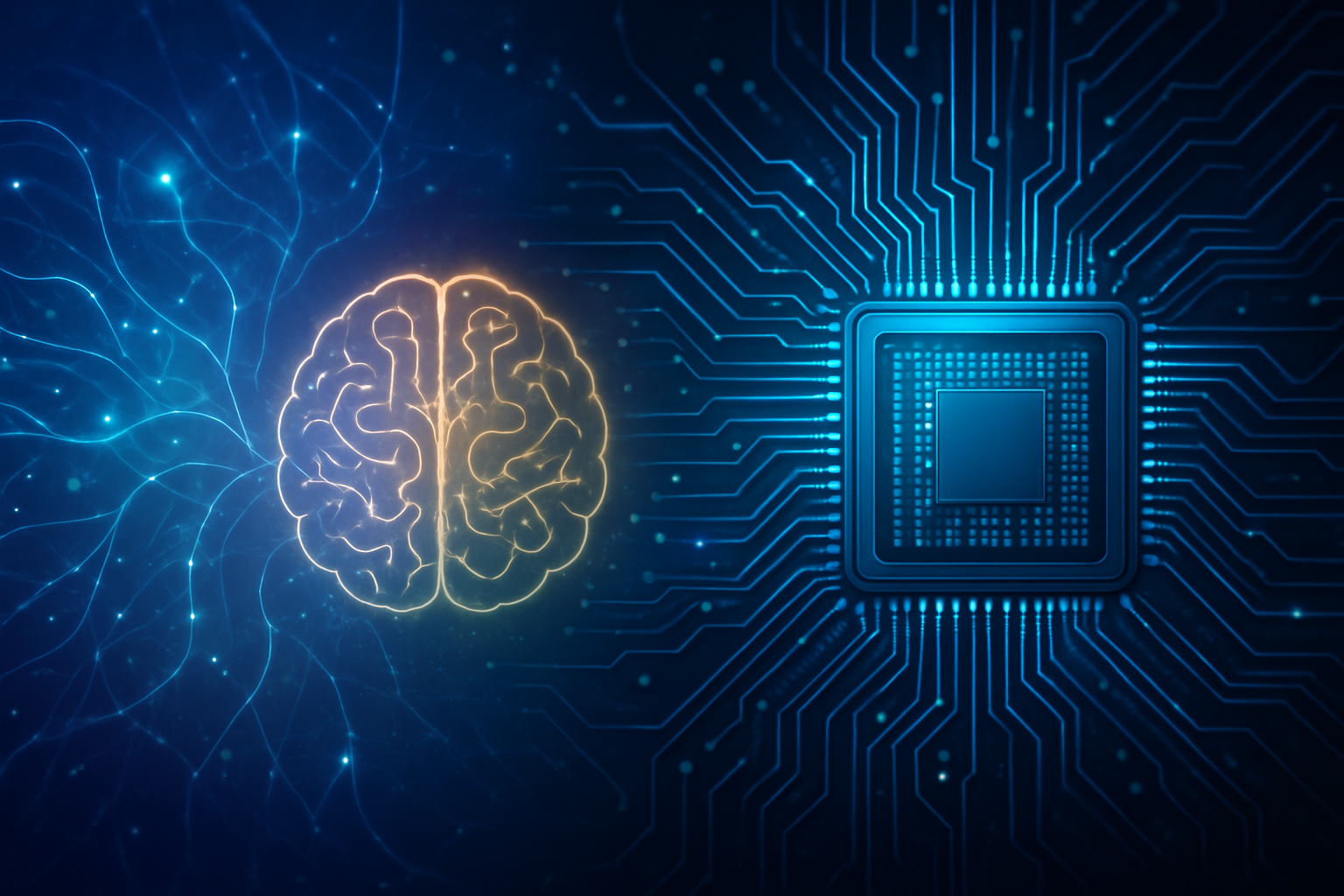
Technical Foundations: The AI Engines Driving Construction Forward
The technical advancements in AI for construction in 2025 are both diverse and deeply impactful, representing a significant departure from previous, more rudimentary approaches. At the forefront are AI and Machine Learning (ML) algorithms that have revolutionized project management. These sophisticated tools leverage vast datasets to predict potential delays, optimize costs through intricate data analysis, and enhance safety protocols with remarkable precision. Predictive analytics, in particular, has become a cornerstone, enabling managers to forecast and mitigate risks proactively, thereby improving project profitability and reducing unforeseen complications.
Generative AI stands as another transformative force, particularly in the design and planning phases. This cutting-edge technology employs algorithms to rapidly create a multitude of design options based on specified parameters, allowing architects and engineers to explore a far wider range of possibilities with unprecedented speed. This not only streamlines creative processes but also optimizes functionality, aesthetics, and sustainability, while significantly reducing human error. AI-powered generative design tools are now routinely optimizing architectural, structural, and subsystem designs, directly contributing to reduced material waste and enhanced buildability. This contrasts sharply with traditional manual design processes, which were often iterative, time-consuming, and limited in scope.
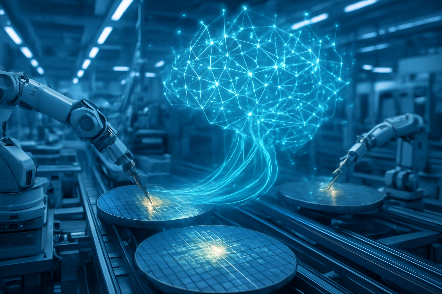
Robotics and automation, intrinsically linked with AI, have become integral to construction sites. Autonomous machines are increasingly performing repetitive and dangerous tasks such as bricklaying, welding, and 3D printing. This leads to faster construction times, reduced labor costs, and improved quality through precise execution. Furthermore, AI-powered computer vision and sensor systems are redefining site safety. These systems continuously monitor job sites for hazards, detect non-compliance with safety measures (e.g., improper helmet use), and alert teams in real time, dramatically reducing accidents. This proactive, real-time monitoring represents a significant leap from reactive safety inspections. Finally, AI is revolutionizing Building Information Modeling (BIM) by integrating predictive analytics, performance monitoring, and advanced building virtualization, enhancing data-driven decision-making and enabling rapid design standardization and validation.
Corporate Landscape: Beneficiaries and Disruptors
The rapid integration of AI into construction has created a dynamic competitive landscape, with established tech giants, specialized AI firms, and innovative startups vying for market leadership. Companies that have successfully embraced and developed AI-powered solutions stand to benefit immensely. For instance, Mastt is gaining traction with its AI-powered cost tracking, risk control, and dashboard solutions tailored for capital project owners. Similarly, Togal.AI is making waves with its AI-driven takeoff and estimating directly from blueprints, significantly accelerating bid processes and improving accuracy for contractors.
ALICE Technologies is a prime example of a company leveraging generative AI for complex construction scheduling and planning, allowing for sophisticated scenario modeling and optimization that was previously unimaginable. In the legal and contractual realm, Document Crunch utilizes AI for contract risk analysis and automated clause detection, streamlining workflows for legal and contract teams. Major construction players are also internalizing AI capabilities; Obayashi Corporation launched AiCorb, a generative design tool that instantly creates façade options and auto-generates 3D BIM models from simple sketches. Bouygues Construction is leveraging AI for design engineering to reduce material waste—reportedly cutting 140 tonnes of steel on a metro project—and using AI-driven schedule simulations to improve project speed and reduce delivery risk.
The competitive implications are clear: companies that fail to adopt AI risk falling behind in efficiency, cost-effectiveness, and safety. AI platforms like Slate Technologies, which deliver up to 15% productivity improvements and a 60% reduction in rework, are becoming indispensable, potentially saving major contractors over $18 million per project. Slate's recent partnership with CMC Project Solutions in December 2025 further underscores the strategic importance of expanding access to advanced project intelligence. Furthermore, HKT is integrating 5G, AI, and IoT to deliver advanced solutions like the Smart Site Safety System (4S), particularly in Hong Kong, showcasing the convergence of multiple cutting-edge technologies. The startup ecosystem is vibrant, with companies like Konstruksi.AI, Renalto, Wenti Labs, BLDX, and Volve demonstrating the breadth of innovation and potential disruption across various construction sub-sectors.
Broader Significance: A New Era for the Built Environment
The pervasive integration of AI into construction signifies a monumental shift in the broader AI landscape, demonstrating the technology's maturity and its capacity to revolutionize traditionally conservative industries. This development is not merely incremental; it represents a fundamental transition from reactive problem-solving to proactive risk mitigation and predictive management across all phases of construction. The ability to anticipate material shortages, schedule conflicts, and equipment breakdowns with greater accuracy fundamentally transforms project delivery.
One of the most significant impacts of AI in construction is its crucial role in addressing the severe global labor shortage facing the industry. By automating repetitive tasks and enhancing overall efficiency, AI allows the existing workforce to focus on higher-value activities, effectively augmenting human capabilities rather than simply replacing them. This strategic application of AI is vital for maintaining productivity and growth in a challenging labor market. The tangible benefits are compelling: AI-powered systems are consistently demonstrating productivity improvements of up to 15% and a remarkable 60% reduction in rework, translating into substantial cost savings and improved project profitability.
Beyond economics, AI is setting new benchmarks for jobsite safety. AI-based safety monitoring, exemplified by KOLON Benit's AI Vision Intelligence system deployed on KOLON GLOBAL's construction sites, is becoming standard practice, fostering a more mindful and secure culture among workers. The continuous, intelligent oversight provided by AI significantly reduces the risk of accidents and ensures compliance with safety protocols. This data-driven approach to decision-making is now central to planning, resource allocation, and on-site execution, marking a profound change from intuition-based or experience-dependent methods. The increased investment in construction-focused AI solutions further underscores the industry's recognition of AI as a critical driver for future success and sustainability.
The Horizon: Future Developments and Uncharted Territory
Looking ahead, the trajectory of AI in construction promises even more transformative developments. Near-term expectations include the widespread adoption of pervasive predictive analytics, which will become a default capability for all major construction projects, enabling unprecedented foresight and control. Generative design tools are anticipated to scale further, moving beyond initial design concepts to fully automated creation of detailed 3D BIM models directly from high-level specifications, drastically accelerating the pre-construction phase.
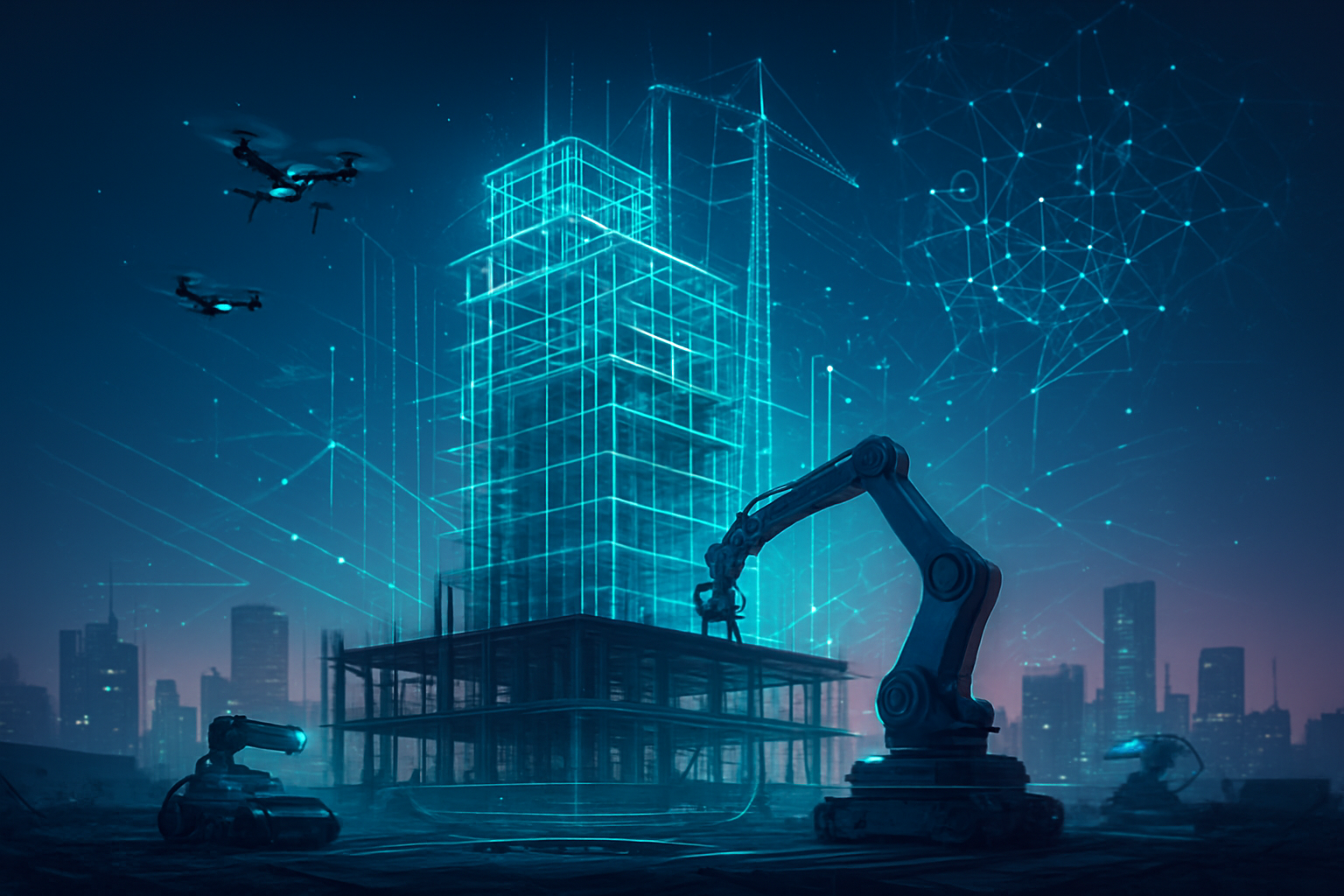
On the long-term horizon, we can expect the deeper integration of autonomous equipment. Autonomous excavators, cranes, and other construction robots will not only handle digging and material tasks but will increasingly coordinate complex operations with minimal human oversight, leading to highly efficient and safe automated construction sites. The vision of fully integrated IoT-enabled smart buildings, where sensors and AI continuously monitor and adjust systems for optimal energy consumption, security, and occupant comfort, is rapidly becoming a reality. These buildings will be self-optimizing ecosystems, responding dynamically to environmental conditions and user needs.
However, challenges remain. The interoperability of diverse AI systems from different vendors, the need for robust cybersecurity measures to protect sensitive project data, and the upskilling of the construction workforce to effectively manage and interact with AI tools are critical areas that need to be addressed. Experts predict a future where AI acts as a universal co-pilot for construction professionals, providing intelligent assistance at every level, from strategic planning to on-site execution. The development of more intuitive conversational AI interfaces will further streamline data interactions, allowing project managers and field workers to access critical information and insights through natural language commands, enhancing decision-making and collaboration.
Concluding Thoughts: AI's Enduring Legacy in Construction
In summary, December 2025 marks a pivotal moment where AI has matured into an indispensable, transformative force within the construction technology sector. The key takeaways from this year include the widespread adoption of predictive analytics, the revolutionary impact of generative AI on design, the increasing prevalence of robotics and automation, and the profound improvements in site safety and efficiency. These advancements collectively represent a shift from reactive to proactive project management, addressing critical industry challenges such as labor shortages and cost overruns.
The significance of these developments in the history of AI is profound. They demonstrate AI's ability to move beyond niche applications and deliver tangible, large-scale benefits in a traditionally conservative, capital-intensive industry. This year's breakthroughs are not merely incremental improvements but foundational changes that are redefining how structures are designed, built, and managed. The long-term impact will be a safer, more sustainable, and significantly more efficient construction industry, capable of delivering complex projects with unprecedented precision and speed.
As we move into the coming weeks and months, the industry should watch for continued advancements in autonomous construction equipment, further integration of AI with BIM platforms, and the emergence of even more sophisticated generative AI tools. The focus will also be on developing comprehensive training programs to equip the workforce with the necessary skills to leverage these powerful new technologies effectively. The future of construction is inextricably linked with AI, promising an era of intelligent building that will reshape our urban landscapes and infrastructure for generations to come.
This content is intended for informational purposes only and represents analysis of current AI developments.
TokenRing AI delivers enterprise-grade solutions for multi-agent AI workflow orchestration, AI-powered development tools, and seamless remote collaboration platforms.
For more information, visit https://www.tokenring.ai/.