Tag: AI

  • The Silicon Fortress Under Siege: Cybersecurity and AI’s Dual Dance in the Semiconductor Ecosystem

    The Silicon Fortress Under Siege: Cybersecurity and AI’s Dual Dance in the Semiconductor Ecosystem

    The foundational layer of modern technology, the semiconductor ecosystem, finds itself at the epicenter of an escalating cybersecurity crisis. This intricate global network, responsible for producing the chips that power everything from smartphones to critical infrastructure and advanced AI systems, is a prime target for sophisticated cybercriminals and state-sponsored actors. The integrity of its intellectual property (IP) and the resilience of its supply chain are under unprecedented threat, demanding robust, proactive measures. At the heart of this battle lies Artificial Intelligence (AI), a double-edged sword that simultaneously introduces novel vulnerabilities and offers cutting-edge defensive capabilities, reshaping the future of digital security.

    Recent incidents, including significant ransomware attacks and alleged IP thefts, underscore the urgency of the situation. With the semiconductor market projected to reach over $800 billion by 2028, the stakes are immense, impacting economic stability, national security, and the very pace of technological innovation. As of December 12, 2025, the industry is in a critical phase, racing to implement advanced cybersecurity protocols while grappling with the complex implications of AI's pervasive influence.

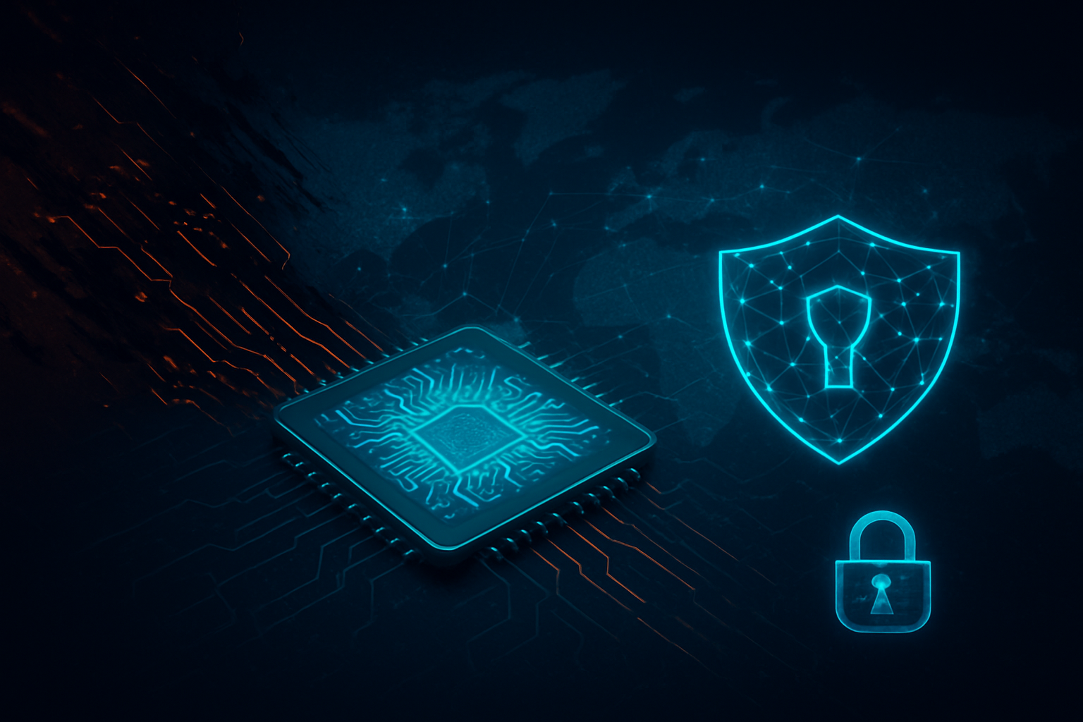
    Hardening the Core: Technical Frontiers in Semiconductor Cybersecurity

    Cybersecurity in the semiconductor ecosystem is a distinct and rapidly evolving field, far removed from traditional software security. It necessitates embedding security deep within the silicon, from the earliest design phases through manufacturing and deployment—a "security by design" philosophy. This approach is a stark departure from historical practices where security was often an afterthought.

    Specific technical measures now include Hardware Security Modules (HSMs) and Trusted Execution Environments (TEEs) like Intel SGX (NASDAQ: INTC) and AMD SEV (NASDAQ: AMD), which create isolated, secure zones within processors. Physically Unclonable Functions (PUFs) leverage unique manufacturing variations to create device-specific cryptographic keys, making each chip distinct and difficult to clone. Secure Boot Mechanisms ensure only authenticated firmware runs, while Formal Verification uses mathematical proofs to validate design security pre-fabrication.

    The industry is also rallying around new standards, such as the SEMI E187 (Specification for Cybersecurity of Fab Equipment), SEMI E188 (Specification for Malware Free Equipment Integration), and the recently published SEMI E191 (Specification for SECS-II Protocol for Computing Device Cybersecurity Status Reporting) from October 2024. These standards mandate baseline cybersecurity requirements for fabrication equipment and data reporting, aiming to secure the entire manufacturing process. TSMC (NYSE: TSM), a leading foundry, has already integrated SEMI E187 into its procurement contracts, signaling a practical shift towards enforcing higher security baselines across its supply chain.

    However, sophisticated vulnerabilities persist. Side-Channel Attacks (SCAs) exploit physical emanations like power consumption or electromagnetic radiation to extract cryptographic keys, a method discovered in 1996 that profoundly changed hardware security. Firmware Vulnerabilities, often stemming from insecure update processes or software bugs (e.g., CWE-347, CWE-345, CWE-287), remain a significant attack surface. Hardware Trojans (HTs), malicious modifications inserted during design or manufacturing, are exceptionally difficult to detect due to the complexity of integrated circuits.

    The research community is highly engaged, with NIST data showing a more than 15-fold increase in hardware-related Common Vulnerabilities and Exposures (CVEs) in the last five years. Collaborative efforts, including the NIST Cybersecurity Framework 2.0 Semiconductor Manufacturing Profile (NIST IR 8546), are working to establish comprehensive, risk-based approaches to managing cyber risks.

    AI's Dual Role: AI presents a paradox in this technical landscape. On one hand, AI-driven chip design and Electronic Design Automation (EDA) tools introduce new vulnerabilities like model extraction, inversion attacks, and adversarial machine learning (AML), where subtle data manipulations can lead to erroneous chip behaviors. AI can also be leveraged to design and embed sophisticated Hardware Trojans at the pre-design stage, making them nearly undetectable. On the other hand, AI is an indispensable defense mechanism. AI and Machine Learning (ML) algorithms offer real-time anomaly detection, processing vast amounts of data to identify and predict threats, including zero-day exploits, with unparalleled speed. ML techniques can also counter SCAs by analyzing microarchitectural features. AI-powered tools are enhancing automated security testing and verification, allowing for granular inspection of hardware and proactive vulnerability prediction, shifting security from a reactive to a proactive stance.

    Corporate Battlegrounds: Impact on Tech Giants, AI Innovators, and Startups

    The escalating cybersecurity concerns in the semiconductor ecosystem profoundly impact companies across the technological spectrum, reshaping competitive landscapes and strategic priorities.

    Tech Giants, many of whom design their own custom chips or rely on leading foundries, are particularly exposed. Companies like Nvidia (NASDAQ: NVDA), a dominant force in GPU design crucial for AI, and Broadcom (NASDAQ: AVGO), a key supplier of custom AI accelerators, are central to the AI market and thus significant targets for IP theft. A single breach can lead to billions in losses and a severe erosion of competitive advantage, as demonstrated by the 2023 MKS Instruments ransomware breach that impacted Applied Materials (NASDAQ: AMAT), causing substantial financial losses and operational shutdowns. These giants must invest heavily in securing their extensive IP portfolios and complex global supply chains, often internalizing security expertise or acquiring specialized cybersecurity firms.

    AI Companies are heavily reliant on advanced semiconductors for training and deploying their models. Any disruption in the supply chain directly stalls AI progress, leading to slower development cycles and constrained deployment of advanced applications. Their proprietary algorithms and sensitive code are prime targets for data leaks, and their AI models are vulnerable to adversarial attacks like data poisoning.

    Startups in the AI space, while benefiting from powerful AI products and services from tech giants, face significant challenges. They often lack the extensive resources and dedicated cybersecurity teams of larger corporations, making them more vulnerable to IP theft and supply chain compromises. The cost of implementing advanced security protocols can be prohibitive, hindering their ability to innovate and compete effectively.

    Companies poised to benefit are those that proactively embed security throughout their operations. Semiconductor manufacturers like TSMC and Intel (NASDAQ: INTC) are investing heavily in domestic production and enhanced security, bolstering supply chain resilience. Cybersecurity solution providers, particularly those leveraging AI and ML for threat detection and incident response, are becoming critical partners. The "AI in Cybersecurity" market is projected for rapid growth, benefiting companies like Cisco Systems (NASDAQ: CSCO), Dell (NYSE: DELL), Palo Alto Networks (NASDAQ: PANW), and HCL Technologies (NSE: HCLTECH). Electronic Design Automation (EDA) tool vendors like Cadence (NASDAQ: CDNS) and Synopsys (NASDAQ: SNPS) that integrate AI for security assurance, such as through acquisitions like Arteris Inc.'s (NASDAQ: AIP) acquisition of Cycuity, will also gain strategic advantages by offering inherently more secure design platforms.

    The competitive landscape is being redefined. Control over the semiconductor supply chain is now a strategic asset, influencing geopolitical power. Companies demonstrating superior cybersecurity and supply chain resilience will differentiate themselves, attracting business from critical sectors like defense and automotive. Conversely, those with weak security postures risk losing market share, facing regulatory penalties, and suffering reputational damage. Strategic advantages will be gained through hardware-level security integration, adoption of zero-trust architectures, investment in AI for cybersecurity, robust supply chain risk management, and active participation in industry collaborations.

    A New Geopolitical Chessboard: Wider Significance and Societal Stakes

    The cybersecurity challenges within the semiconductor ecosystem, amplified by AI's dual nature, extend far beyond corporate balance sheets, profoundly impacting national security, economic stability, and societal well-being. This current juncture represents a strategic urgency comparable to previous technological milestones.

    National Security is inextricably linked to semiconductor security. Chips are the backbone of modern military systems, critical infrastructure (from communication networks to power grids), and advanced defense technologies, including AI-driven weapons. A disruption in the supply of critical semiconductors or a compromise of their integrity could cripple a nation's defense capabilities and undermine its technological superiority. Geopolitical tensions and trade wars further highlight the urgent need for nations to diversify supply chains and strengthen domestic semiconductor production capabilities, as seen with multi-billion dollar initiatives like the U.S. CHIPS Act and the EU Chips Act.

    Economic Stability is also at risk. The semiconductor industry drives global economic growth, supporting countless jobs and industries. Disruptions from cyberattacks or supply chain vulnerabilities can lead to massive financial losses, production halts across various sectors (as witnessed during the 2020-2021 global chip shortage), and eroded trust. The industry's projected growth to surpass US$1 trillion by 2030 underscores its critical economic importance, making its security a global economic imperative.

    Societal Concerns stemming from AI's dual role are also significant. AI systems can inadvertently leak sensitive training data, and AI-powered tools can enable mass surveillance, raising privacy concerns. Biases in AI algorithms, learned from skewed data, can lead to discriminatory outcomes. Furthermore, generative AI facilitates the creation of deepfakes for scams and propaganda, and the spread of AI-generated misinformation ("hallucinations"), posing risks to public trust and societal cohesion. The increasing integration of AI into critical operational technology (OT) environments also introduces new vulnerabilities that could have real-world physical impacts.

    This era mirrors past technological races, such as the development of early computing infrastructure or the internet's proliferation. Just as high-bandwidth memory (HBM) became pivotal for the explosion of large language models (LLMs) and the current "AI supercycle," the security of the underlying silicon is now recognized as foundational for the integrity and trustworthiness of all future AI-powered systems. The continuous innovation in semiconductor architecture, including GPUs, TPUs, and NPUs, is crucial for advancing AI capabilities, but only if these components are inherently secure.

    The Horizon of Defense: Future Developments and Expert Predictions

    The future of semiconductor cybersecurity is a dynamic interplay between advancing threats and innovative defenses, with AI at the forefront of both. Experts predict robust long-term growth for the semiconductor market, exceeding US$1 trillion by the end of the decade, largely driven by AI and IoT technologies. However, this growth is inextricably linked to managing escalating cybersecurity risks.

    In the near term (next 1-3 years), the industry will intensify its focus on Zero Trust Architecture to minimize lateral movement in networks, enhanced supply chain risk management through thorough vendor assessments and secure procurement, and advanced threat detection using AI and ML. Proactive measures like employee training, regular audits, and secure hardware design with built-in features will become standard. Adherence to global regulatory frameworks like ISO/IEC 27001 and the EU's Cyber Resilience Act will also be crucial.

    Looking to the long term (3+ years), we can expect the emergence of quantum cryptography to prepare for a post-quantum era, blockchain technology to enhance supply chain transparency and security, and fully AI-driven autonomous cybersecurity solutions capable of anticipating attacker moves and automating responses at machine speed. Agentic AI, capable of autonomous multi-step workflows, will likely be deployed for advanced threat hunting and vulnerability prediction. Further advancements in security access layers and future-proof cryptographic algorithms embedded directly into chip architecture are also anticipated.

    Potential applications for robust semiconductor cybersecurity span numerous critical sectors: automotive (protecting autonomous vehicles), healthcare (securing medical devices), telecommunications (safeguarding 5G networks), consumer electronics, and critical infrastructure (protecting power grids and transportation from AI-physical reality convergence attacks). The core use cases will remain IP protection and ensuring supply chain integrity against malicious hardware or counterfeit products.

    Significant challenges persist, including the inherent complexity of global supply chains, the persistent threat of IP theft, the prevalence of legacy systems, the rapidly evolving threat landscape, and a lack of consistent standardization. The high cost of implementing robust security and a persistent talent gap in cybersecurity professionals with semiconductor expertise also pose hurdles.

    Experts predict a continuous surge in demand for AI-driven cybersecurity solutions, with AI spending alone forecast to hit $1.5 trillion in 2025. The manufacturing sector, including semiconductors, will remain a top target for cyberattacks, with ransomware and DDoS incidents expected to escalate. Innovations in semiconductor design will include on-chip optical communication, continued memory advancements (e.g., HBM, GDDR7), and backside power delivery.

    AI's dual role will only intensify. As a solution, AI will provide enhanced threat detection, predictive analytics, automated security operations, and advanced hardware security testing. As a threat, AI will enable more sophisticated adversarial machine learning, AI-generated hardware Trojans, and autonomous cyber warfare, potentially leading to AI-versus-AI combat scenarios.

    Fortifying the Future: A Comprehensive Wrap-up

    The semiconductor ecosystem stands at a critical juncture, navigating an unprecedented wave of cybersecurity threats that target its invaluable intellectual property and complex global supply chain. This foundational industry, vital for every aspect of modern life, is facing a sophisticated and ever-evolving adversary. Artificial Intelligence, while a primary driver of demand for advanced chips, simultaneously presents itself as both the architect of new vulnerabilities and the most potent tool for defense.

    Key takeaways underscore the industry's vulnerability as a high-value target for nation-state espionage and ransomware. The global and interconnected nature of the supply chain presents significant attack surfaces, susceptible to geopolitical tensions and malicious insertions. Crucially, AI's double-edged nature means it can be weaponized for advanced attacks, such as AI-generated hardware Trojans and adversarial machine learning, but it is also indispensable for real-time threat detection, predictive security, and automated design verification. The path forward demands unprecedented collaboration, shared security standards, and robust measures across the entire value chain.

    This development marks a pivotal moment in AI history. The "AI supercycle" is fueling an insatiable demand for computational power, making the security of the underlying AI chips paramount for the integrity and trustworthiness of all AI-powered systems. The symbiotic relationship between AI advancements and semiconductor innovation means that securing the silicon is synonymous with securing the future of AI itself.

    In the long term, the fusion of AI and semiconductor innovation will be essential for fortifying digital infrastructures worldwide. We can anticipate a continuous loop where more secure, AI-designed chips enable more robust AI-powered cybersecurity, leading to a more resilient digital landscape. However, this will be an ongoing "AI arms race," requiring sustained investment in advanced security solutions, cross-disciplinary expertise, and international collaboration to stay ahead of malicious actors. The drive for domestic manufacturing and diversification of supply chains, spurred by both cybersecurity and geopolitical concerns, will fundamentally reshape the global semiconductor landscape, prioritizing security alongside efficiency.

    What to watch for in the coming weeks and months: Expect continued geopolitical activity and targeted attacks on key semiconductor regions, particularly those aimed at IP theft. Monitor the evolution of AI-powered cyberattacks, especially those involving subtle manipulation of chip designs or firmware. Look for further progress in establishing common cybersecurity standards and collaborative initiatives within the semiconductor industry, as evidenced by forums like SEMICON Korea 2026. Keep an eye on the deployment of more advanced AI and machine learning solutions for real-time threat detection and automated incident response. Finally, observe governmental policies and private sector investments aimed at strengthening domestic semiconductor manufacturing and supply chain security, as these will heavily influence the industry's future direction and resilience.


    This content is intended for informational purposes only and represents analysis of current AI developments.

    TokenRing AI delivers enterprise-grade solutions for multi-agent AI workflow orchestration, AI-powered development tools, and seamless remote collaboration platforms.
    For more information, visit https://www.tokenring.ai/.

  • Beyond Moore’s Law: Advanced Packaging and Miniaturization Propel the Future of AI and Computing

    Beyond Moore’s Law: Advanced Packaging and Miniaturization Propel the Future of AI and Computing

    As of December 2025, the semiconductor industry stands at a pivotal juncture, navigating the evolving landscape where traditional silicon scaling, once the bedrock of technological advancement, faces increasing physical and economic hurdles. In response, a powerful dual strategy of relentless chip miniaturization and groundbreaking advanced packaging technologies has emerged as the new frontier, driving unprecedented improvements in performance, power efficiency, and device form factor. This synergistic approach is not merely extending the life of Moore's Law but fundamentally redefining how processing power is delivered, with profound implications for everything from artificial intelligence to consumer electronics.

    The immediate significance of these advancements cannot be overstated. With the insatiable demand for computational horsepower driven by generative AI, high-performance computing (HPC), and the ever-expanding Internet of Things (IoT), the ability to pack more functionality into smaller, more efficient packages is critical. Advanced packaging, in particular, has transitioned from a supportive process to a core architectural enabler, allowing for the integration of diverse chiplets and components into sophisticated "mini-systems." This paradigm shift is crucial for overcoming bottlenecks like the "memory wall" and unlocking the next generation of intelligent, ubiquitous technology.

    The Architecture of Tomorrow: Unpacking Advanced Semiconductor Technologies

    The current wave of semiconductor innovation is characterized by a sophisticated interplay of nanoscale fabrication and ingenious integration techniques. While the pursuit of smaller transistors continues, with manufacturers pushing into 3-nanometer (nm) and 2nm processes—and Intel (NASDAQ: INTC) targeting 1.8nm mass production by 2026—the true revolution lies in how these tiny components are assembled. This contrasts sharply with previous eras where monolithic chip design and simple packaging sufficed.

    At the forefront of this technical evolution are several key advanced packaging technologies:

    • 2.5D Integration: This technique involves placing multiple chiplets side-by-side on a silicon or organic interposer within a single package. It facilitates high-bandwidth communication between different dies, effectively bypassing the reticle limit (the maximum size of a single chip that can be manufactured monolithically). Leading examples include TSMC's (TPE: 2330) CoWoS, Samsung's (KRX: 005930) I-Cube, and Intel's (NASDAQ: INTC) EMIB. This differs from traditional packaging by enabling much tighter integration and higher data transfer rates between adjacent chips.
    • 3D Stacking / 3D-IC: A more aggressive approach, 3D stacking involves vertically layering multiple dies—such as logic, memory, and sensors—and interconnecting them with Through-Silicon Vias (TSVs). TSVs are tiny vertical electrical connections that dramatically shorten data travel distances, significantly boosting bandwidth and reducing power consumption. High Bandwidth Memory (HBM), essential for AI accelerators, is a prime example, placing vast amounts of memory directly atop or adjacent to the processing unit. This vertical integration offers a far smaller footprint and superior performance compared to traditional side-by-side placement of discrete components.
    • Chiplets: These are small, modular integrated circuits that can be combined and interconnected to form a complete system. This modularity offers unprecedented design flexibility, allowing designers to mix and match specialized chiplets (e.g., CPU, GPU, I/O, memory controllers) from different process nodes or even different manufacturers. This approach significantly reduces development time and cost, improves manufacturing yields by isolating defects to smaller components, and enables custom solutions for specific applications. It represents a departure from the "system-on-a-chip" (SoC) philosophy by distributing functionality across multiple, specialized dies.
    • System-in-Package (SiP) and Wafer-Level Packaging (WLP): SiP integrates multiple ICs and passive components into a single package for compact, efficient designs, particularly in mobile and IoT devices. WLP and Fan-Out Wafer-Level Packaging (FO-WLP/FO-PLP) package chips directly at the wafer level, leading to smaller, more power-efficient packages with increased input/output density.

    Initial reactions from the AI research community and industry experts are overwhelmingly positive. The consensus is that advanced packaging is no longer merely an optimization but a fundamental requirement for pushing the boundaries of AI, especially with the emergence of large language models and generative AI. The ability to overcome memory bottlenecks and deliver unprecedented bandwidth is seen as critical for training and deploying increasingly complex AI models. Experts highlight the necessity of co-designing chips and their packaging from the outset, rather than treating packaging as an afterthought, to fully realize the potential of these technologies.

    Reshaping the Competitive Landscape: Who Benefits and Who Adapts?

    The advancements in miniaturization and advanced packaging are profoundly reshaping the competitive dynamics within the semiconductor and broader technology industries. Companies with significant R&D investments and established capabilities in these areas stand to gain substantial strategic advantages, while others will need to rapidly adapt or risk falling behind.

    Leading semiconductor manufacturers like Taiwan Semiconductor Manufacturing Company (TSMC) (TPE: 2330), Intel Corporation (NASDAQ: INTC), and Samsung Electronics Co., Ltd. (KRX: 005930) are at the forefront, heavily investing in and expanding their advanced packaging capacities. TSMC, with its CoWoS (Chip-on-Wafer-on-Substrate) and InFO (Integrated Fan-Out) technologies, has become a critical enabler for AI chip developers, including NVIDIA Corporation (NASDAQ: NVDA) and Advanced Micro Devices, Inc. (NASDAQ: AMD). These foundries are not just manufacturing chips but are now integral partners in designing the entire system-in-package, offering competitive differentiation through their packaging expertise.

    NVIDIA (NASDAQ: NVDA) and AMD (NASDAQ: AMD) are prime beneficiaries, leveraging 2.5D and 3D stacking with HBM to power their cutting-edge GPUs and AI accelerators. Their ability to deliver unparalleled memory bandwidth and computational density directly stems from these packaging innovations, giving them a significant edge in the booming AI and high-performance computing markets. Similarly, memory giants like Micron Technology, Inc. (NASDAQ: MU) and SK Hynix Inc. (KRX: 000660), which produce HBM, are seeing surging demand and investing heavily in next-generation 3D memory stacks.

    The competitive implications are significant for major AI labs and tech giants. Companies developing their own custom AI silicon, such as Alphabet Inc. (NASDAQ: GOOG, GOOGL) with its TPUs and Amazon.com, Inc. (NASDAQ: AMZN) with its Graviton and Trainium chips, are increasingly relying on advanced packaging to optimize their designs for specific workloads. This allows them to achieve superior performance-per-watt and cost efficiency compared to off-the-shelf solutions.

    Potential disruption to existing products or services includes a shift away from purely monolithic chip designs towards more modular, chiplet-based architectures. This could democratize chip design to some extent, allowing smaller startups to innovate by integrating specialized chiplets without the prohibitively high costs of designing an entire SoC from scratch. However, it also creates a new set of challenges related to chiplet interoperability and standardization. Companies that fail to embrace heterogeneous integration and advanced packaging risk being outmaneuvered by competitors who can deliver more powerful, compact, and energy-efficient solutions across various market segments, from data centers to edge devices.

    A New Era of Computing: Wider Significance and Broader Trends

    The relentless pursuit of miniaturization and the rise of advanced packaging technologies are not isolated developments; they represent a fundamental shift in the broader AI and computing landscape, ushering in what many are calling the "More than Moore" era. This paradigm acknowledges that performance gains are now derived not just from shrinking transistors but equally from innovative architectural and packaging solutions.

    This trend fits perfectly into the broader AI landscape, where the sheer scale of data and complexity of models demand unprecedented computational resources. Advanced packaging directly addresses critical bottlenecks, particularly the "memory wall," which has long limited the performance of AI accelerators. By placing memory closer to the processing units, these technologies enable faster data access, higher bandwidth, and lower latency, which are absolutely essential for training and inference of large language models (LLMs), generative AI, and complex neural networks. The market for generative AI chips alone is projected to exceed $150 billion in 2025, underscoring the critical role of these packaging innovations.

    The impacts extend far beyond AI. In consumer electronics, these advancements are enabling smaller, more powerful, and energy-efficient mobile devices, wearables, and IoT sensors. The automotive industry, with its rapidly evolving autonomous driving and electric vehicle technologies, also heavily relies on high-performance, compact semiconductor solutions for advanced driver-assistance systems (ADAS) and AI-powered control units.

    While the benefits are immense, potential concerns include the increasing complexity and cost of manufacturing. Advanced packaging processes require highly specialized equipment, materials, and expertise, leading to higher development and production costs. Thermal management for densely packed 3D stacks also presents significant engineering challenges, as heat dissipation becomes more difficult in confined spaces. Furthermore, the burgeoning chiplet ecosystem necessitates robust standardization efforts to ensure interoperability and foster a truly open and competitive market.

    Compared to previous AI milestones, such as the initial breakthroughs in deep learning or the development of specialized AI accelerators, the current focus on packaging represents a foundational shift. It's not just about algorithmic innovation or new chip architectures; it's about the very physical realization of those innovations, enabling them to reach their full potential. This emphasis on integration and efficiency is as critical as any algorithmic breakthrough in driving the next wave of AI capabilities.

    The Road Ahead: Future Developments and Expert Predictions

    The trajectory of miniaturization and advanced packaging points towards an exciting future, with continuous innovation expected in both the near and long term. Experts predict a future where chip design and packaging are inextricably linked, co-architected from the ground up to optimize performance, power, and cost.

    In the near term, we can expect further refinement and widespread adoption of existing advanced packaging technologies. This includes the maturation of 2nm and even 1.8nm process nodes, coupled with more sophisticated 2.5D and 3D integration techniques. Innovations in materials science will play a crucial role, with developments in glass interposers offering superior electrical and thermal properties compared to silicon, and new high-performance thermal interface materials addressing heat dissipation challenges in dense stacks. The standardization of chiplet interfaces, such as UCIe (Universal Chiplet Interconnect Express), is also expected to gain significant traction, fostering a more open and modular ecosystem for chip design.

    Longer-term developments include the exploration of truly revolutionary approaches like Holographic Metasurface Nano-Lithography (HMNL), a new 3D printing method that could enable entirely new 3D package architectures and previously impossible designs, such as fully 3D-printed electronic packages or components integrated into unconventional spaces. The concept of "system-on-package" (SoP) will evolve further, integrating not just digital and analog components but also optical and even biological elements into highly compact, functional units.

    Potential applications and use cases on the horizon are vast. Beyond more powerful AI and HPC, these technologies will enable hyper-miniaturized sensors for ubiquitous IoT, advanced medical implants, and next-generation augmented and virtual reality devices with unprecedented display resolutions and processing power. Autonomous systems, from vehicles to drones, will benefit from highly integrated, robust, and power-efficient processing units.

    Challenges that need to be addressed include the escalating cost of advanced manufacturing facilities, the complexity of design and verification for heterogeneous integrated systems, and the ongoing need for improved thermal management solutions. Experts predict a continued consolidation in the advanced packaging market, with major players investing heavily to capture market share. They also foresee a greater emphasis on sustainability in manufacturing processes, given the environmental impact of chip production. The drive for "disaggregated computing" – breaking down large processors into smaller, specialized chiplets – will continue, pushing the boundaries of what's possible in terms of customization and efficiency.

    A Defining Moment for the Semiconductor Industry

    In summary, the confluence of continuous chip miniaturization and advanced packaging technologies represents a defining moment in the history of the semiconductor industry. As traditional scaling approaches encounter fundamental limits, these innovative strategies have become the primary engines for driving performance improvements, power efficiency, and form factor reduction across the entire spectrum of electronic devices. The transition from monolithic chips to modular, heterogeneously integrated systems marks a profound shift, enabling the exponential growth of artificial intelligence, high-performance computing, and a myriad of other transformative technologies.

    This development's significance in AI history is paramount. It addresses the physical bottlenecks that could otherwise stifle the progress of increasingly complex AI models, particularly in the realm of generative AI and large language models. By enabling higher bandwidth, lower latency, and greater computational density, advanced packaging is directly facilitating the next generation of AI capabilities, from faster training to more efficient inference at the edge.

    Looking ahead, the long-term impact will be a world where computing is even more pervasive, powerful, and seamlessly integrated into our lives. Devices will become smarter, smaller, and more energy-efficient, unlocking new possibilities in health, communication, and automation. What to watch for in the coming weeks and months includes further announcements from leading foundries regarding their next-generation packaging roadmaps, new product launches from AI chip developers leveraging these advanced techniques, and continued efforts towards standardization within the chiplet ecosystem. The race to integrate more, faster, and smaller components is on, and the outcomes will shape the technological landscape for decades to come.


    This content is intended for informational purposes only and represents analysis of current AI developments.

    TokenRing AI delivers enterprise-grade solutions for multi-agent AI workflow orchestration, AI-powered development tools, and seamless remote collaboration platforms.
    For more information, visit https://www.tokenring.ai/.

  • The Looming Silicon Ceiling: Semiconductor Talent Shortage Threatens Global AI Ambitions

    The Looming Silicon Ceiling: Semiconductor Talent Shortage Threatens Global AI Ambitions

    The global semiconductor industry, the foundational bedrock of the modern digital economy and the AI era, is facing an unprecedented and escalating talent shortage. This critical deficit, projected to require over one million additional skilled workers worldwide by 2030, threatens to impede innovation, disrupt global supply chains, and undermine economic growth and national security. The scarcity of highly specialized engineers, technicians, and even skilled tradespeople is creating a "silicon ceiling" that could significantly constrain the rapid advancement of Artificial Intelligence and other transformative technologies.

    This crisis is not merely a temporary blip but a deep, structural issue fueled by explosive demand for chips across sectors like AI, 5G, and automotive, coupled with an aging workforce and an insufficient pipeline of new talent. The immediate significance is profound: new fabrication plants (fabs) risk operating under capacity or sitting idle, product development cycles face delays, and the industry's ability to meet surging global demand for advanced processors is compromised. As AI enters a "supercycle," the human capital required to design, manufacture, and operate the hardware powering this revolution is becoming the single most critical bottleneck.

    Unpacking the Technical Divide: Skill Gaps and a New Era of Scarcity

    The current semiconductor talent crisis is distinct from previous industry challenges, marked by a unique confluence of factors and specific technical skill gaps. Unlike past cyclical downturns, this shortage is driven by an unprecedented, sustained surge in demand, coupled with a fundamental shift in required expertise.

    Specific technical skill gaps are pervasive across the industry. There is an urgent need for advanced engineering and design skills, particularly in AI, system engineering, quantum computing, and data science. Professionals are sought after for AI-specific chip architectures, edge AI processing, and deep knowledge of machine learning and advanced packaging technologies. Core technical skills in device physics, advanced process technology, IC design and verification (analog, digital, RF, and mixed-signal), 3D integration, and advanced assembly are also in high demand. A critical gap exists in hardware-software integration, with a significant need for "hybrid skill sets" that bridge traditional electrical and materials engineering with data science and machine learning. In advanced manufacturing, expertise in complex processes like extreme ultraviolet (EUV) lithography and 3D chip stacking is scarce, as is the need for semiconductor materials scientists. Testing and automation roles require proficiency in tools like Python, LabVIEW, and MATLAB, alongside expertise in RF and optical testing. Even skilled tradespeople—electrians, pipefitters, and welders—are in short supply for constructing new fabs.

    This shortage differs from historical challenges due to its scale and nature. The industry is experiencing exponential growth, projected to reach $2 trillion by 2030, demanding approximately 100,000 new hires annually, a scale far exceeding previous growth cycles. Decades of outsourcing manufacturing have led to significant gaps in domestic talent pools in countries like the U.S. and Europe, making reshoring efforts difficult. The aging workforce, with a third of U.S. semiconductor employees aged 55 or older nearing retirement, signifies a massive loss of institutional knowledge. Furthermore, the rapid integration of automation and AI means skill requirements are constantly shifting, demanding workers who can collaborate with advanced systems. The educational pipeline remains inadequate, failing to produce enough graduates with job-ready skills.

    Initial reactions from the AI research community and industry experts underscore the severity. AI is seen as an indispensable tool for managing complexity but also as a primary driver exacerbating the talent shortage. Experts view the crisis as a long-term structural problem, evolving beyond simple silicon shortages to "hidden shortages deeper in the supply chain," posing a macroeconomic risk that could slow AI-based productivity gains. There is a strong consensus on the urgency of rearchitecting work processes and developing new talent pipelines, with governments responding through significant investments like the U.S. CHIPS and Science Act and the EU Chips Act.

    Competitive Battlegrounds: Impact on Tech Giants, AI Innovators, and Startups

    The semiconductor talent shortage is reshaping the competitive landscape across the tech industry, creating clear winners and losers among AI companies, tech giants, and nimble startups. The "war for talent" is intensifying, with profound implications for product development, market positioning, and strategic advantages.

    Tech giants with substantial resources and foresight, such as NVIDIA (NASDAQ: NVDA), Intel (NASDAQ: INTC), Amazon (NASDAQ: AMZN), and Google (NASDAQ: GOOGL), are better positioned to navigate this crisis. Companies like Amazon and Google have invested heavily in designing their own in-house AI chips, offering a degree of insulation from external supply chain disruptions and talent scarcity. This capability allows them to customize hardware for their specific AI workloads, reducing reliance on third-party suppliers and attracting top-tier design talent. Intel, with its robust manufacturing capabilities and significant investments in foundry services, aims to benefit from reshoring initiatives, though it too faces immense talent challenges. These larger players can also offer more competitive compensation packages, benefits, and robust career development programs, making them attractive to a limited pool of highly skilled professionals.

    Conversely, smaller AI-native startups and companies heavily reliant on external, traditional supply chains are at a significant disadvantage. Startups often struggle to match the compensation and benefits offered by industry giants, hindering their ability to attract the specialized talent needed for cutting-edge AI hardware and software integration. They also face intense competition for scarce generative AI services and the underlying hardware, particularly GPUs. Companies without in-house chip design capabilities or diversified sourcing strategies will likely experience increased costs, extended lead times, and the risk of losing market share due to persistent semiconductor shortages. The delay in new fabrication plant operationalization, as seen with TSMC (NYSE: TSM) in Arizona due to talent shortages, exemplifies the broad impact across the supply chain.

    The competitive implications are stark. The talent shortage intensifies global competition for engineering and research talent, leading to escalating wages for specialized skills, which disproportionately affects smaller firms. This crisis is also accelerating a shift towards national self-reliance strategies, with countries investing in domestic production and talent development, potentially altering global supply chain dynamics. Companies that fail to adapt their talent and supply chain strategies risk higher costs and lost market share. Market positioning strategies now revolve around aggressive talent development and retention, strategic recruitment partnerships with educational institutions, rebranding the industry to attract younger generations, and leveraging AI/ML for workforce planning and automation to mitigate human resource bottlenecks.

    A Foundational Challenge: Wider Significance and Societal Ripples

    The semiconductor talent shortage transcends immediate industry concerns, posing a foundational challenge with far-reaching implications for the broader AI landscape, technological sovereignty, national security, and societal well-being. Its significance draws parallels to pivotal moments in industrial history, underscoring its role as a critical bottleneck for the digital age.

    Within the broader AI landscape, the talent deficit creates innovation bottlenecks, threatening to slow the pace of AI technological advancement. Without sufficient skilled workers to design and manufacture next-generation semiconductors, the development and deployment of new AI technologies, from advanced consumer products to critical infrastructure, will be constrained. This could force greater reliance on generalized hardware, limiting the efficiency and performance of bespoke AI solutions and potentially consolidating power among a few dominant players like NVIDIA (NASDAQ: NVDA), who can secure top-tier talent and cutting-edge manufacturing. The future of AI is profoundly dependent not just on algorithmic breakthroughs but equally on the human capital capable of innovating the hardware that powers it.

    For technological sovereignty and national security, semiconductors are now recognized as strategic assets. The talent shortage exacerbates geopolitical vulnerabilities, particularly for nations dependent on foreign foundries. Efforts to reshore manufacturing, such as those driven by the U.S. CHIPS and Science Act and the European Chips Act, are critically undermined if there aren't enough skilled workers to operate these advanced facilities. A lack of domestic talent directly impacts a country's ability to produce critical components for defense systems and innovate in strategic technologies, as semiconductors are dual-use technologies. The erosion of domestic manufacturing expertise over decades, with production moving offshore, has contributed to this talent gap, making rebuilding efforts challenging.

    Societal concerns also emerge. If efforts to diversify hiring and educational outreach don't keep pace, the talent shortage could exacerbate existing inequalities. The intense pressure on a limited pool of skilled workers can lead to burnout and retention issues, impacting overall productivity. Increased competition for talent can drive up production costs, which are likely to be passed on to consumers, resulting in higher prices for technology-dependent products. The industry also struggles with a "perception gap," with many younger engineers gravitating towards "sexier" software jobs, compounding the issue of an aging workforce nearing retirement.

    Historically, this challenge resonates with periods where foundational technologies faced skill bottlenecks. Similar to the pivotal role of steam power or electricity, semiconductors are the bedrock of the modern digital economy. A talent shortage here impedes progress across an entire spectrum of dependent industries, much like a lack of skilled engineers would have hindered earlier industrial revolutions. The current crisis is a "structural issue" driven by long-brewing factors, demanding systemic societal and educational reforms akin to those required to support entirely new industrial paradigms in the past.

    The Road Ahead: Future Developments and Expert Outlook

    Addressing the semiconductor talent shortage requires a multi-faceted approach, encompassing both near-term interventions and long-term strategic developments. The industry, academia, and governments are collaborating to forge new pathways and mitigate the looming "silicon ceiling."

    In the near term, the focus is on pragmatic strategies to quickly augment the workforce and improve retention. Companies are expanding recruitment efforts to adjacent industries like aerospace, automotive, and medical devices, seeking professionals with transferable skills. Significant investment is being made in upskilling and reskilling existing employees through educational assistance and targeted certifications. AI-driven recruitment tools are streamlining hiring, while partnerships with community colleges and technical schools are providing hands-on learning and internships to build entry-level talent pipelines. Companies are also enhancing benefits, offering flexible work arrangements, and improving workplace culture to attract and retain talent.

    Long-term developments involve more foundational changes. This includes developing new talent pipelines through comprehensive STEM education programs starting at high school and collegiate levels, specifically designed for semiconductor careers. Strategic workforce planning aims to identify and develop future skills, taking into account the impact of global policies like the CHIPS Act. There's a deep integration of automation and AI, not just to boost efficiency but also to manage tasks that are difficult to staff, including AI-driven systems for precision manufacturing and design. Diversity, Equity, and Inclusion (DEI) and Environmental, Social, and Governance (ESG) initiatives are gaining prominence to broaden the talent pool and foster inclusive environments. Knowledge transfer and retention programs are crucial to capture the tacit knowledge of an aging workforce.

    Potential applications and use cases on the horizon include AI optimizing talent sourcing and dynamically matching candidates with industry needs. Digital twins and virtual reality are being deployed in educational institutions to provide students with hands-on experience on expensive equipment, accelerating their readiness for industry roles. AI-enhanced manufacturing and design will simplify chip development, lower production costs, and accelerate time-to-market. Robotics and cobots will handle delicate wafers in fabs, while AI for operational efficiency will monitor and adjust processes, predict deviations, and analyze supply chain data.

    However, significant challenges remain. Universities struggle to keep pace with evolving skill requirements, and the aging workforce poses a continuous threat of knowledge loss. The semiconductor industry still battles a perception problem, often seen as less appealing than software giants, making talent acquisition difficult. Restrictive immigration policies can hinder access to global talent, and the high costs and time associated with training are hurdles for many companies. Experts, including those from Deloitte and SEMI, predict a persistent global talent gap of over one million skilled workers by 2030, with the U.S. alone facing a shortfall of 59,000 to 146,000 workers by 2029. The demand for engineers is expected to worsen until planned programs provide increased supply, likely around 2028. The industry's success hinges on its ability to fundamentally shift its approach to workforce development.

    The Human Factor: A Comprehensive Wrap-up on Semiconductor's Future

    The global semiconductor talent shortage is not merely an operational challenge; it is a profound structural impediment that will define the trajectory of technological advancement, particularly in Artificial Intelligence, for decades to come. With projections indicating a need for over one million additional skilled workers globally by 2030, the industry faces a monumental task that demands a unified and innovative response.

    This crisis holds immense significance in AI history. As AI becomes the primary demand driver for advanced semiconductors, the availability of human capital to design, manufacture, and innovate these chips is paramount. The talent shortage risks creating a hardware bottleneck that could slow the exponential growth of AI, particularly large language models and generative AI. It serves as a stark reminder that hardware innovation and human capital development are just as critical as software advancements in enabling the next wave of technological progress. Paradoxically, AI itself is emerging as a potential solution, with AI-driven tools automating complex tasks and augmenting human capabilities, thereby expanding the talent pool and allowing engineers to focus on higher-value innovation.

    The long-term impact of an unaddressed talent shortage is dire. It threatens to stifle innovation, impede global economic growth, and compromise national security by undermining efforts to achieve technological sovereignty. Massive investments in new fabrication plants and R&D centers risk being underutilized without a sufficient skilled workforce. The industry must undergo a systemic transformation in its approach to workforce development, strengthening educational pipelines, attracting diverse talent, and investing heavily in continuous learning and reskilling programs.

    In the coming weeks and months, watch for an increase in public-private partnerships and educational initiatives aimed at establishing new training programs and university curricula. Expect more aggressive recruitment and retention strategies from semiconductor companies, focusing on improving workplace culture and offering competitive packages. The integration of AI in workforce solutions, from talent acquisition to employee upskilling, will likely accelerate. Ongoing GPU shortages and updates on new fab capacity timelines will continue to be critical indicators of the industry's ability to meet demand. Finally, geopolitical developments will continue to shape supply chain strategies and impact talent mobility, underscoring the strategic importance of this human capital challenge. The semiconductor industry is at a crossroads, and its ability to cultivate, attract, and retain the specialized human capital will determine the pace of global technological progress and the full realization of the AI revolution.


    This content is intended for informational purposes only and represents analysis of current AI developments.

    TokenRing AI delivers enterprise-grade solutions for multi-agent AI workflow orchestration, AI-powered development tools, and seamless remote collaboration platforms.
    For more information, visit https://www.tokenring.ai/.

  • The Green Revolution in Silicon: Semiconductor Manufacturing Embraces Sustainability

    The Green Revolution in Silicon: Semiconductor Manufacturing Embraces Sustainability

    The semiconductor industry, the foundational bedrock of our digital world and the engine powering the explosive growth of artificial intelligence, is undergoing a profound transformation. Driven by escalating environmental concerns, stringent regulatory demands, and a heightened sense of corporate responsibility, chip manufacturers are increasingly prioritizing energy efficiency and sustainable practices in every facet of chip fabrication. This paradigm shift is not merely an environmental obligation but a strategic imperative, crucial for mitigating climate change, conserving vital resources, and ensuring the long-term viability and social license of an industry projected to exceed $1 trillion by 2030.

    This concerted push towards "green semiconductor manufacturing" holds immediate and far-reaching significance. For the industry, it translates into reduced operational costs through optimized energy and water usage, enhanced brand reputation amidst growing consumer and corporate demand for eco-friendly products, and crucial compliance with evolving global environmental regulations. Environmentally, these initiatives promise a substantial reduction in greenhouse gas emissions, critical water conservation in water-stressed regions, minimized hazardous waste generation, and a decreased reliance on virgin resources through circular economy principles. As AI's computational demands skyrocket, the sustainability of its underlying hardware becomes paramount, making green chip production a cornerstone of a responsible technological future.

    Engineering a Greener Future: Technical Innovations in Chip Fabrication

    The pivot towards sustainable semiconductor manufacturing is underpinned by a wave of technical innovations spanning equipment, processes, materials, water management, and waste reduction, fundamentally altering traditional, resource-intensive methods.

    In energy efficiency, modern "green fabs" are designed with advanced HVAC systems, optimized cleanroom environments, and intelligent energy management features in equipment, allowing devices to enter low-power states during idle periods – a stark contrast to older, continuously high-consumption machinery. AI and machine learning (AI/ML) are increasingly leveraged to optimize chip designs, predict and control energy consumption in real-time, and enhance production efficiency. Furthermore, leading manufacturers are rapidly integrating renewable energy sources like solar and wind power, reducing reliance on fossil fuels. While cutting-edge technologies like Extreme Ultraviolet (EUV) lithography are highly energy-intensive (over 10 times older methods), the broader focus is on holistic energy reduction.

    The material landscape is also evolving. Wide-Bandgap (WBG) materials like Gallium Nitride (GaN) and Silicon Carbide (SiC) are gaining prominence. These materials offer superior energy efficiency, handling higher voltages and temperatures than traditional silicon, leading to more efficient power electronics crucial for electric vehicles and data centers. Research into organic semiconductors, bio-based polymers, and recycled materials aims to reduce toxicity and resource demand.

    Water management is seeing revolutionary advancements. Historically, a single silicon wafer could require up to 3,000 liters of ultrapure water. Today, companies are investing in multi-stage filtration, reverse osmosis (RO), and membrane bioreactors to recycle and reuse process water, with some achieving 98% recycling rates. Closed-loop water systems and dry processing techniques like plasma-based etching are minimizing freshwater consumption, moving away from chemical-intensive pH RO and conventional wet cleaning.

    For waste reduction, innovative chemical recycling processes are recovering valuable materials like sulfuric acid and solvents, significantly cutting down on disposal costs and the need for new chemicals. Process optimization, material substitution, and ozone cleaning are reducing hazardous waste generation. Comprehensive recycling programs for solid waste, including plastic packaging, are becoming standard, a significant departure from historical practices of simply disposing of spent chemicals and materials.

    Industry experts widely acknowledge the urgency. The International Energy Agency (IEA) projects a 4-6% annual increase in the electronics sector's energy consumption, underscoring the need for these efficiencies. While Deloitte (NYSE: DLTE) predicts a 15% decrease in energy consumption per dollar of revenue by 2024 due to renewable energy, current commitments are deemed insufficient to meet net-zero goals by 2050, with emissions projected to overshoot the 1.5°C pathway by 3.5 times. Collaborative efforts like the Semiconductor Climate Consortium (SCC) and the International Electronics Manufacturing Initiative (iNEMI) are crucial for developing and scaling sustainable solutions and establishing life cycle assessment frameworks.

    Reshaping the Tech Landscape: Impact on Giants and Startups

    The green revolution in semiconductor manufacturing is not just an operational shift; it's a strategic pivot that is reshaping the competitive dynamics for AI companies, tech giants, and nascent startups alike.

    Major players already heavily invested in sustainable practices are poised to reap significant benefits. Taiwan Semiconductor Manufacturing Company (TSMC: TPE: 2330), the world's largest contract chipmaker, is a prime example. Their ambitious goals to reduce emissions by 2040, integrate green hydrogen, and invest in on-site water electrolysis directly impact the entire tech ecosystem relying on their advanced chips. Similarly, Intel (NASDAQ: INTC) has adopted a holistic sustainability approach, aiming for net-zero GHG emissions for Scope 1 and 2 by 2040 and Scope 3 by 2050, and already utilizes 99% renewable energy. Their collaboration with Merck (NYSE: MRK) on AI-driven sustainable processes further solidifies their leadership. Samsung (KRX: 005930) is actively reducing its carbon footprint and partnering with NVIDIA (NASDAQ: NVDA) to develop AI-powered semiconductor factories using digital twins for operational planning and anomaly detection, enhancing efficiency and reducing environmental impact. NVIDIA itself is pushing for renewable energy adoption and developing energy-efficient systems for AI workloads, which can be up to 20 times more efficient than CPU-only systems for AI inference and training.

    This shift creates a first-mover advantage for companies that proactively invest in green manufacturing, securing cost savings, improving brand image, and ensuring compliance. Conversely, the high initial investment costs for upgrading or building green fabs pose increased barriers to entry for smaller players. Sustainability is fast becoming a key differentiator, especially as corporate clients like Apple (NASDAQ: AAPL) and Daimler (FWB: DAI) demand net-zero supply chains from their semiconductor partners. This drives new collaborations across the value chain, fostering ecosystem development.

    The push for energy-efficient chip design is directly linked to green manufacturing, potentially disrupting existing product designs by favoring alternative materials like GaN and SiC over traditional silicon for certain applications. Supply chains are being redesigned to prioritize eco-friendly materials and traceability, possibly phasing out hazardous chemicals. New service offerings focused on chip recycling and refurbishment are emerging, while AI companies developing tools to optimize manufacturing processes, monitor energy usage, and manage supply chain emissions will see increased demand for their services.

    Strategically, companies demonstrating leadership in sustainable manufacturing can achieve enhanced market positioning as responsible innovators, attracting green capital and benefiting from government incentives like the US CHIPS and Science Act and the EU Chips Act. This also mitigates risks associated with regulatory penalties and resource scarcity. The challenges of green manufacturing act as an innovation catalyst, driving R&D into proprietary green technologies. Crucially, tech giants whose products rely on advanced semiconductors will increasingly prioritize suppliers with strong sustainability credentials, creating a powerful market pull for green chips throughout the value chain.

    A Broader Canvas: AI, Environment, and Society

    The greening of semiconductor manufacturing extends far beyond the factory floor, weaving into the broader AI landscape and influencing environmental, economic, and societal trends.

    Environmentally, these initiatives are critical for reining in the industry's substantial footprint. They aim to reduce the billions of kilowatt-hours consumed by fabs annually, minimize the vast quantities of ultrapure water needed, decrease the use and release of hazardous chemicals (including potent fluorinated gases), and combat the growing tide of electronic waste. The transition to renewable energy sources and advanced recycling systems directly combats climate change and resource depletion.

    Economically, while initial investments are high, the long-term gains are significant. Reduced energy and water bills, optimized resource usage, and efficient waste management translate into substantial cost savings. Enhanced brand reputation and competitive advantage in an eco-conscious market attract investment and customer loyalty. Proactive regulatory compliance mitigates financial and reputational risks. Moreover, the pursuit of green manufacturing sparks innovation, creating new market opportunities in sustainable materials and processes.

    Societally, these efforts safeguard public health by reducing pollution and hazardous chemical exposure. They contribute to resource security, particularly water, in regions often facing scarcity. By promoting responsible consumption and production, they align with global Sustainable Development Goals. Critically, green semiconductors are foundational enablers of other green technologies—electric vehicles, renewable energy systems, and smart grids—accelerating the global transition to a decarbonized economy.

    However, concerns persist. The high initial investment for green upgrades, the complexity of global supply chains, and the constant challenge of balancing performance with sustainability remain significant hurdles. The rebound effect, where increased efficiency leads to greater overall consumption, also poses a risk.

    This entire movement is inextricably linked to the broader AI landscape. AI's insatiable demand for computational power translates into an urgent need for "green chips"—energy-efficient semiconductors. Without them, the energy footprint of AI, particularly from data centers and generative AI models, would become unsustainable. Conversely, AI itself is a powerful enabler for green manufacturing, optimizing processes, managing resources, and even designing more energy-efficient chips. This symbiotic relationship underpins the emerging "Green AI" trend, which aims to minimize AI's own environmental footprint through optimized algorithms, smaller models, low-power hardware, and renewable energy-powered data centers.

    Compared to previous AI milestones, this era marks a significant evolution. Early AI had a negligible environmental footprint. The deep learning era saw growing computational demands, but environmental scrutiny was nascent. Today's generative AI, with its unprecedented energy consumption, has brought AI's environmental impact to the forefront, making sustainable manufacturing a strategic imperative. The key difference is that AI is now not only recognized for its environmental impact but is also being actively leveraged as a powerful tool for environmental sustainability, a mature and responsible approach to technological development.

    The Horizon: Future Developments and Expert Predictions

    The trajectory of green semiconductor manufacturing points towards a future defined by continuous innovation, systemic integration of sustainability, and a relentless pursuit of net-zero operations.

    In the near-term (1-5 years), expect accelerated renewable energy integration, with more chipmakers committing to 100% renewable energy targets by 2030 and beyond. Water conservation and recycling will intensify, driven by stricter regulations and technological breakthroughs enabling ultra-high recycling rates. Energy-efficient chip architectures will become standard, with continued innovation in low-power transistors and power-gating. Process optimization and automation, heavily augmented by AI, will further refine manufacturing to minimize environmental impact. Furthermore, green procurement and supply chain optimization will see wider adoption, reducing Scope 3 emissions across the value chain.

    Long-term developments (beyond 5 years) will focus on more transformative shifts. The widespread adoption of circular economy principles will emphasize robust systems for recycling, reusing, and repurposing materials from end-of-life chips. Green chemistry and sustainable materials will see significant breakthroughs, replacing toxic chemicals and exploring biodegradable electronics. The ultimate goal is a low-carbon energy transition for all fabs, potentially even integrating advanced nuclear power solutions for immense energy demands. A holistic value chain transformation will encompass every stage, from raw material extraction to product end-of-life.

    These green semiconductors will enable a host of future applications. They are fundamental for renewable energy systems, making solar and wind power more efficient. They are critical for electric vehicles (EVs) and their charging infrastructure, optimizing battery performance and energy conversion. Energy-efficient data centers will rely on low-power processors to reduce their colossal energy footprint. The widespread deployment of Internet of Things (IoT) devices and smart grids will also heavily depend on these sustainable chips.

    However, significant challenges remain. The sheer energy and water intensity of advanced manufacturing nodes, particularly EUV lithography, continues to be a hurdle. Greenhouse gas emissions, especially from fluorinated compounds, are projected to grow, with AI-driven chip manufacturing alone potentially contributing 16 million metric tons of CO₂ by 2030. The high cost of green transition, complex global supply chains, and the ongoing e-waste crisis demand sustained effort and investment. Technical barriers to integrating novel, sustainable materials into highly precise manufacturing processes also need to be overcome.

    Experts predict a complex but determined path forward. TechInsights forecasts that carbon emissions from semiconductor manufacturing will continue to rise, reaching 277 million metric tons of CO2e by 2030, with AI accelerators being a major contributor. Yet, this will be met by accelerated sustainability commitments, with more top companies announcing ambitious net-zero targets. AI is expected to play an even more pivotal role as a sustainability enabler, optimizing designs and manufacturing. The shift to smart manufacturing will intensify, integrating energy-efficient equipment, renewables, automation, and AI. Regulatory frameworks like the EU's Ecodesign for Sustainable Products Regulation (ESPR) will be key drivers. While Moore's Law has historically driven efficiency, future focus will also be on green chemistry and new materials.

    A Sustainable Silicon Future: Concluding Thoughts

    The journey towards sustainability in semiconductor manufacturing is a defining chapter in the history of technology. It underscores a critical realization: that the relentless pursuit of technological advancement, particularly in fields as transformative as AI, must be harmonized with an equally fervent commitment to environmental stewardship.

    The key takeaways are clear: the industry is actively engaged in a multi-pronged effort to reduce its environmental footprint through energy efficiency, water conservation, waste reduction, and supply chain sustainability. This is not a superficial trend but a deep-seated transformation driven by economic necessity, regulatory pressure, and ethical responsibility. Its significance in AI history is profound; green semiconductor manufacturing is the essential, often unseen, foundation upon which a truly sustainable AI future can be built. Without greener chips, the exponential growth of AI's computational demands risks exacerbating global climate challenges. Conversely, AI itself is proving to be an indispensable ally in achieving these green manufacturing goals.

    The long-term impact will be a fundamentally greener and more resilient tech ecosystem. Sustainability will be ingrained as a core principle, leading to a continuous cycle of innovation in materials, processes, and energy sources. This will not only de-risk the industry from resource scarcity and regulatory penalties but also empower the broader global transition to a decarbonized economy by providing the sustainable components needed for renewable energy, EVs, and smart infrastructure.

    In the coming weeks and months, watch for intensified efforts in renewable energy adoption, with major fabs announcing new projects and reaching significant milestones. The expansion of AI-driven optimization within factories will be a crucial trend, as will increased scrutiny and concrete actions on Scope 3 emissions across supply chains. Keep an eye on evolving regulatory frameworks, particularly from the EU, which are likely to set new benchmarks for sustainable product design and material use. The ongoing development and deployment of advanced water stewardship innovations will also be critical, especially in regions facing water stress. The alignment of technological prowess with ecological responsibility is not just a desirable outcome; it is the imperative for a sustainable silicon future.


    This content is intended for informational purposes only and represents analysis of current AI developments.

    TokenRing AI delivers enterprise-grade solutions for multi-agent AI workflow orchestration, AI-powered development tools, and seamless remote collaboration platforms.
    For more information, visit https://www.tokenring.ai/.

  • Quantum Revolution: How Entangled Bits Are Reshaping the Future of Chip Development

    Quantum Revolution: How Entangled Bits Are Reshaping the Future of Chip Development

    The world of computing stands on the precipice of a monumental shift, driven by the enigmatic power of quantum mechanics. Quantum computing, once a theoretical marvel, is rapidly emerging as a transformative force set to fundamentally redefine semiconductor design, capabilities, and even the very materials that constitute our chips. This isn't merely an incremental upgrade; it's a paradigm shift promising to unlock computational powers previously unimaginable for classical machines, accelerating innovation across both quantum and conventional semiconductor technologies.

    At its core, quantum computing harnesses phenomena like superposition and entanglement, allowing qubits to exist in multiple states simultaneously and be interconnected in ways impossible for classical bits. This capability enables quantum computers to tackle problems intractable for even the most powerful supercomputers, ranging from complex material simulations to intricate optimization challenges critical for advanced chip layouts. The immediate significance for the tech industry is profound, as this nascent field acts as a powerful catalyst, compelling leading companies and startups alike to innovate at an unprecedented pace, promising a future where chips are vastly more powerful, efficient, and capable of solving humanity's most complex challenges.

    The Quantum Leap in Semiconductor Engineering

    The technical ramifications of quantum computing on chip development are both deep and broad, promising to revolutionize every facet from conceptual design to physical fabrication. Quantum-powered AI, for instance, is already proving its mettle in accelerating the development of advanced semiconductor architectures and optimizing complex manufacturing processes. Australian researchers have validated quantum machine learning models that outperform classical AI in simulating critical fabrication steps like ohmic contact resistance, leading to potential increases in yield and reductions in costs for both classical and future quantum chips.

    This differs significantly from previous approaches by moving beyond the classical binary limitations, enabling computations at speeds orders of magnitude faster. Quantum systems facilitate the design of innovative structures such as 3D chips and neuromorphic processors, which mimic the human brain's architecture, leading to faster, more energy-efficient chips capable of supporting cutting-edge technologies like advanced AI and the burgeoning Internet of Things (IoT). Moreover, quantum simulators can model material behavior at an atomic level, leading to the discovery of new materials with superior properties for chip fabrication, such as advanced silicon-based qubits with improved stability, strained germanium for cooler and faster chips, and even superconducting germanium-gallium for integrated quantum-classical circuits. Initial reactions from the AI research community and industry experts highlight a mix of excitement and cautious optimism, recognizing the immense potential while acknowledging the significant engineering and scientific hurdles that remain, particularly in achieving robust quantum error correction and scalability.

    Corporate Giants and Nimble Startups in the Quantum Race

    The race to harness quantum computing's influence on chip development has galvanized tech giants and a vibrant ecosystem of startups, each vying for a strategic advantage in this nascent but potentially trillion-dollar market. Companies like IBM (NYSE: IBM), a long-standing leader, continues to advance its superconducting qubit technology, with processors like Eagle (127 qubits) and the forthcoming Condor (1,121 qubits), while investing billions in R&D to bolster manufacturing of quantum and mainframe computers. Google, having famously claimed "quantum supremacy" with its Sycamore processor, pushes boundaries with its Willow chip, which recently demonstrated significant breakthroughs in quantum error correction by halving error rates and achieving a verifiable "quantum advantage" by running an algorithm 13,000 times faster than the world's fastest supercomputer.

    Intel (NASDAQ: INTC), leveraging its vast semiconductor manufacturing expertise, focuses on silicon spin qubits, aiming for scalability through existing fabrication infrastructure, exemplified by its 12-qubit Tunnel Falls chip. More recently, Amazon (NASDAQ: AMZN) officially entered the quantum chip race in early 2025 with AWS Ocelot, developed in partnership with Caltech, complementing its AWS Braket cloud quantum service. Microsoft (NASDAQ: MSFT), through its Azure Quantum platform, provides cloud access to quantum hardware from partners like IonQ (NYSE: IONQ) and Rigetti Computing (NASDAQ: RGTI), while also developing its own quantum programming languages like Q#. Publicly traded quantum specialists like IonQ (trapped ions) and Rigetti Computing (superconducting qubits) are at the forefront of hardware development, offering their systems via cloud platforms. D-Wave Quantum (NYSE: QBTS) continues to lead in quantum annealing.

    The competitive landscape is further enriched by numerous startups specializing in various qubit technologies—from superconducting (IQM, QuantWare) and photonic (Xanadu, Quandela) to neutral atoms (Atom Computing, PASQAL) and silicon quantum dots (Diraq). These companies are not only developing new hardware but also crucial software, error correction tools (Q-Ctrl, Nord Quantique), and specialized applications. This intense competition, coupled with strategic partnerships and significant government funding, creates a dynamic environment. The potential disruption to existing products and services is immense: quantum computing could render some traditional semiconductor designs obsolete for certain tasks, accelerate AI development far beyond current classical limits, revolutionize drug discovery, and even necessitate a complete overhaul of current cryptographic standards. Companies that can effectively integrate quantum capabilities into their offerings or develop quantum-resistant solutions will secure significant market positioning and strategic advantages in the coming decades.

    Broader Implications and Societal Crossroads

    Quantum computing's influence on chip development extends far beyond the confines of laboratories and corporate campuses, weaving itself into the broader AI landscape and promising profound societal shifts. It represents not merely an incremental technological advancement but a fundamental paradigm shift, akin to the invention of the transistor or the internet. Unlike previous AI milestones that optimized algorithms on classical hardware, quantum computing offers a fundamentally different approach, with the potential for exponential speedup in specific tasks, such as Shor's algorithm for factoring large numbers, marks a qualitative leap in computational power.

    The societal impacts are multifaceted. Economically, quantum computing is expected to transform entire industries, creating new career paths in quantum algorithm design, post-quantum cryptography, and quantum-AI integration. Industries like pharmaceuticals, finance, logistics, and materials science are poised for revolutionary breakthroughs through optimized processes and accelerated discovery. Scientifically, quantum computers promise to help humanity address grand challenges such as climate change, food insecurity, and disease through advanced simulations and material design. However, this transformative power also brings significant concerns.

    Security risks are paramount, as quantum computers will be capable of breaking many current encryption methods (RSA, ECC), threatening banking, personal data, and government security. The urgent need for a transition to Post-Quantum Cryptography (PQC) is an immediate concern, with adversaries potentially engaging in "harvest now, decrypt later" attacks. Ethical concerns include the potential for quantum AI systems to amplify existing societal biases if trained on biased data, leading to discriminatory outcomes. Data privacy is also a major worry, as immense quantum processing capabilities could make personal information more vulnerable. Economically, the high cost and technical expertise required for quantum computing could widen the digital divide, concentrating power in the hands of a few governments or large corporations, potentially leading to monopolies and increased inequality.

    The Quantum Horizon: Near-Term Progress and Long-Term Visions

    The journey of quantum computing's influence on chip development is marked by a clear roadmap of near-term progress and ambitious long-term visions. In the immediate future (the next few years), the focus remains on advancing quantum error correction (QEC), with significant strides being made to reduce the overhead required for creating stable logical qubits. Companies like IBM are targeting increasingly higher qubit counts, aiming for a quantum-centric supercomputer with over 4,000 qubits by 2025, while Rigetti plans for systems exceeding 100 qubits by the end of the year. The synergy between quantum computing and AI is also expected to deepen, accelerating advancements in optimization, drug discovery, and climate modeling. Experts predict that 2025 will be a pivotal year for QEC, with scalable error-correcting codes beginning to reduce the overhead for fault-tolerant quantum computing.

    Looking further ahead (beyond 5-10 years), the ultimate goal is the realization of fault-tolerant quantum computers, where robust error correction allows for reliable, large-scale computations. IBM aims to deliver such a system by 2029. This era will likely see the blurring of lines between classical and quantum computing, with hybrid architectures becoming commonplace, leading to entirely new classes of computing devices. Potential applications and use cases on the horizon are vast, ranging from highly optimized chip designs and advanced material discovery to revolutionizing semiconductor manufacturing processes, improving supply chain management, and embedding quantum-resistant cryptography directly into hardware. Challenges remain formidable, including qubit fragility and decoherence, the immense overhead of error correction, scalability issues, hardware complexity and cost, and the ongoing talent gap. However, experts like Intel's CEO Pat Gelsinger believe that quantum computing, alongside classical and AI computing, will define the next several decades of technological growth, with quantum systems potentially displacing dominant chip architectures by the end of the decade. The period between 2030 and 2040 is projected for achieving broad quantum advantage, followed by full-scale fault tolerance after 2040, promising a transformative impact across numerous sectors.

    The Quantum Age Dawns: A Transformative Assessment

    The ongoing advancements in quantum computing's influence on chip development represent a pivotal moment in the history of technology. We are witnessing the dawn of a new computational era that promises to transcend the limitations of classical silicon, ushering in capabilities that will reshape industries, accelerate scientific discovery, and redefine our understanding of what is computationally possible. The key takeaway is that quantum computing is not a distant dream; it is actively, and increasingly, shaping the future of chip design and manufacturing, even for classical systems.

    This development's significance in AI history is profound, marking a qualitative leap beyond previous milestones. While deep learning brought remarkable advancements by optimizing algorithms on classical hardware, quantum computing offers a fundamentally different approach, with the potential for exponential speedups in solving problems currently intractable for even the most powerful supercomputers. The long-term impact will be transformative, leading to breakthroughs in fields from personalized medicine and materials science to climate modeling and advanced cybersecurity. However, the journey is not without its challenges, particularly in achieving stable, scalable, and fault-tolerant quantum systems, and addressing the ethical, security, and economic concerns that arise with such powerful technology.

    In the coming weeks and months, watch for continued breakthroughs in quantum error correction, increasing qubit counts, and the emergence of more sophisticated hybrid quantum-classical architectures. Keep an eye on the strategic investments by tech giants and the innovative solutions from a burgeoning ecosystem of startups. The convergence of quantum computing and AI, particularly in the realm of chip development, promises to be one of the most exciting and impactful narratives of the 21st century.


    This content is intended for informational purposes only and represents analysis of current AI developments.

    TokenRing AI delivers enterprise-grade solutions for multi-agent AI workflow orchestration, AI-powered development tools, and seamless remote collaboration platforms.
    For more information, visit https://www.tokenring.ai/.

  • The Great Chip Chase: Reshaping the Global Semiconductor Supply Chain for a Resilient Future

    The Great Chip Chase: Reshaping the Global Semiconductor Supply Chain for a Resilient Future

    The global semiconductor supply chain, the intricate network underpinning nearly every facet of modern technology, is in the throes of a profound transformation. Far from being a static entity, it is currently a battleground where the urgent need for flexibility and reliability clashes with inherent rigidities and escalating external pressures. This ongoing quest for a more robust and responsive supply chain is not merely an industry buzzword; it represents a critical inflection point with immediate and far-reaching implications for the tech industry, national security, and the stability of the global economy.

    The immediate significance of these dynamics cannot be overstated. From the automotive industry facing billions in lost revenue due to chip shortages to consumers experiencing product scarcity and rising prices, the ripple effects are palpable. Geopolitical tensions, concentrated manufacturing capacity, and the lingering impacts of a demand surge have exposed the vulnerabilities of a system once optimized for efficiency over resilience. The current environment necessitates a fundamental rethinking of how semiconductors are designed, manufactured, and distributed, pushing stakeholders towards unprecedented levels of collaboration and strategic investment to safeguard the future of technology.

    Unpacking the Rigidity: Technical Hurdles in Semiconductor Production

    The semiconductor supply chain's inherent lack of flexibility stems from a confluence of highly specialized technical and operational factors. At its core, chip manufacturing is a multi-stage, globe-spanning endeavor involving design, fabrication (wafer processing), assembly, testing, and packaging. Each stage demands highly specialized equipment, unique intellectual property, and often, specific geographic conditions, making rapid adjustments to production schedules exceedingly difficult. The lead time from initial design to final product can span months or even years, rendering the supply chain inherently slow to respond to sudden shifts in demand or unforeseen disruptions.

    A critical technical bottleneck is the heavy reliance on a limited number of advanced foundries, such as Taiwan Semiconductor Manufacturing Company (NYSE: TSM) and Samsung Electronics Co., Ltd. (KRX: 005930). These facilities, operating at peak capacity to meet global demand for cutting-edge chips, leave minimal margin for error or increased output during crises. Any disruption—be it a natural disaster, a power outage, or a geopolitical event—at these pivotal hubs can trigger a cascading effect, causing widespread global shortages. Furthermore, the industry's historical adoption of just-in-time (JIT) inventory practices, while efficient in stable times, has stripped away crucial buffers, transforming minor hiccups into significant supply chain crises. This lack of excess stock means that when a factory line halts due to a missing component, there's often no immediate alternative.

    Achieving greater flexibility and reliability is a formidable technical challenge. It involves not just building more fabs, which require multi-billion-dollar investments and years to construct, but also developing more agile manufacturing processes, enhancing end-to-end supply chain visibility through advanced analytics and AI, and diversifying sourcing of critical raw materials. For instance, the reliance on a few concentrated sources for materials like neon gas (impacted by geopolitical conflicts) or specific rare earth elements highlights the fragility. New approaches are exploring modular manufacturing, advanced simulation tools for risk assessment, and regionalized supply chain models to mitigate dependencies, moving away from a purely globalized, hyper-efficient, but brittle structure towards a more distributed and resilient ecosystem.

    Corporate Chessboard: Impact on Tech Giants, AI Labs, and Startups

    The evolving semiconductor supply chain dynamics are reshaping the competitive landscape for tech giants, AI labs, and startups alike, creating both immense opportunities and significant threats. Companies with strong balance sheets and strategic foresight stand to benefit by investing in supply chain resilience, while others may face significant competitive disadvantages.

    Major tech companies like Apple Inc. (NASDAQ: AAPL), Microsoft Corporation (NASDAQ: MSFT), and Alphabet Inc. (NASDAQ: GOOGL) are heavily reliant on a steady supply of advanced chips for their products and cloud services. These giants are increasingly diversifying their sourcing, investing directly in chip design (e.g., Apple's M-series chips), and even exploring partnerships with foundries to secure dedicated capacity. Companies that can guarantee chip supply will maintain product launch schedules and market share, while those struggling with procurement will face production delays, higher costs, and potential loss of consumer trust. The competitive implication is clear: control over or guaranteed access to semiconductor supply is becoming as critical as software innovation itself.

    For AI labs and startups, the impact is particularly acute. Cutting-edge AI development is heavily dependent on the latest, most powerful GPUs and specialized AI accelerators. Shortages of these high-demand components can cripple research efforts, delay product development, and hinder the ability to scale AI models. Startups, with fewer resources and less purchasing power than established tech giants, are often the first to feel the squeeze, potentially stifling innovation in a rapidly evolving field. This environment could lead to a consolidation of AI development around companies that can secure necessary hardware, or it could spur innovation in more hardware-efficient AI algorithms. Furthermore, the push for regionalization could create opportunities for new domestic semiconductor design and manufacturing startups, fueled by government incentives like the U.S. CHIPS Act.

    The potential for disruption to existing products and services is significant. Companies unable to secure necessary components might be forced to redesign products to use alternative, less optimal chips, leading to performance compromises or delayed releases. Market positioning will increasingly be influenced by supply chain robustness. Companies that demonstrate resilience and can consistently deliver products despite global disruptions will gain a strategic advantage, fostering greater customer loyalty and market confidence. The shift also accelerates the trend towards vertical integration, where companies seek to control more aspects of their hardware supply, from design to potentially even manufacturing, to mitigate external risks.

    Broader Implications: Geopolitics, National Security, and Economic Stability

    The quest for a more flexible and reliable semiconductor supply chain transcends mere corporate strategy; it has profound implications for the broader AI landscape, global geopolitical stability, and national security. Semiconductors are no longer just components; they are strategic assets, often referred to as "geopolitical chess pieces," that dictate economic power, technological leadership, and military advantage.

    This fits squarely into broader AI trends that demand ever-increasing computational power. As AI models grow in complexity and data intensity, the demand for advanced, high-performance chips will only escalate. A brittle supply chain poses a direct threat to the pace of AI innovation, potentially creating chokepoints that could slow the development of critical technologies like autonomous systems, advanced healthcare AI, and next-generation computing. The current situation highlights the interconnectedness of hardware and software—without reliable hardware, even the most groundbreaking AI algorithms remain theoretical.

    The impacts are multi-faceted. Economically, prolonged chip shortages contribute to inflation, hinder industrial output across numerous sectors (e.g., automotive, consumer electronics, industrial IoT), and create systemic risks for global value chains. Geopolitically, the concentration of advanced manufacturing in specific regions, particularly Taiwan, creates vulnerabilities that are a source of international tension. Governments worldwide, recognizing the critical nature of semiconductors, are now actively intervening with massive subsidies and policy initiatives (e.g., the U.S. CHIPS and Science Act, the EU Chips Act) to incentivize domestic manufacturing and diversify global capacity. This marks a significant shift from decades of offshoring and globalization.

    Potential concerns are numerous: the risk of technological decoupling between major powers, the creation of fragmented "chip blocs," and the potential for increased trade protectionism. Comparisons to previous AI milestones underscore the current challenge. While past breakthroughs focused on algorithmic advancements, the current crisis highlights that the physical infrastructure supporting AI is just as crucial. The ability to reliably produce and access advanced chips is now a prerequisite for continued AI progress, making supply chain resilience a foundational element for future AI leadership.

    The Road Ahead: Future Developments and Expert Predictions

    The semiconductor industry is poised for significant transformation as it navigates the imperative for greater flexibility and reliability. In the near term, we can expect continued aggressive investment in new fabrication plants (fabs) across diverse geographies. Companies like Intel Corporation (NASDAQ: INTC), for example, are making substantial commitments to expand manufacturing capabilities in the U.S. and Europe, aiming to rebalance global production. Simultaneously, there will be a strong emphasis on enhancing supply chain visibility through advanced data analytics, AI-driven forecasting, and blockchain technologies to track components from raw material to final product.

    Long-term developments will likely include a push towards greater standardization in certain manufacturing processes and the exploration of new materials and chip architectures that might be less reliant on rare earth elements or highly specialized production techniques. Research into "lights-out" manufacturing, where automation minimizes human intervention, could also contribute to greater efficiency and resilience against labor shortages or disruptions. Furthermore, the concept of "chiplets" – breaking down complex chips into smaller, interconnected modules – could offer more flexibility in design and sourcing, allowing for greater customization and potentially reducing reliance on single, monolithic manufacturing processes.

    Potential applications and use cases on the horizon include the development of AI-powered tools specifically designed to optimize supply chain logistics, predict disruptions before they occur, and dynamically re-route production or sourcing. We might also see the emergence of "digital twins" of entire supply chains, allowing for real-time simulation and stress-testing of various disruption scenarios. Experts predict a shift towards more regionalized supply chains, often referred to as "friend-shoring" or "ally-shoring," where countries collaborate with trusted partners to build robust, redundant manufacturing ecosystems, reducing reliance on potentially adversarial nations or single points of failure.

    However, significant challenges remain. The enormous capital expenditure and long lead times required to build new fabs mean that increasing capacity and achieving true geographical diversification will take years, not months. Talent shortages in semiconductor engineering and manufacturing also pose a persistent hurdle. Experts predict that while the immediate crunch may ease in some sectors, the underlying structural issues will continue to drive strategic investments and policy interventions for the foreseeable future. The goal is not necessarily complete self-sufficiency for every nation, but rather a globally distributed network with sufficient redundancy and resilience to withstand future shocks.

    A New Era of Resilience: Charting the Course for Semiconductors

    The current evolution of the semiconductor supply chain marks a pivotal moment in the history of technology and global commerce. The era of hyper-efficient, lean, and geographically concentrated production, while economically advantageous in stable times, has proven dangerously fragile in the face of unprecedented demand surges, geopolitical tensions, and natural disasters. The key takeaway is clear: resilience and reliability are now paramount, often outweighing pure cost efficiency in strategic importance.

    This development signifies a fundamental re-evaluation of how critical technologies are produced and secured. It underscores that the physical infrastructure of innovation—the factories, the materials, the logistical networks—is as vital as the intellectual breakthroughs themselves. The lessons learned from recent shortages will undoubtedly shape industrial policy, corporate strategy, and international relations for decades to come, moving the industry towards a more robust, diversified, and strategically managed ecosystem.

    What to watch for in the coming weeks and months includes the progress of major government initiatives like the CHIPS Acts in the U.S. and Europe, observing whether these investments translate into tangible increases in domestic manufacturing capacity. Keep an eye on announcements from major semiconductor companies regarding new fab constructions, strategic partnerships, and advancements in supply chain management technologies. Furthermore, monitor geopolitical developments, as they will continue to exert significant influence on trade policies and the push for supply chain diversification. The "Great Chip Chase" is far from over; it is entering a new, more strategic phase, with profound implications for the future of AI and the global economy.


    This content is intended for informational purposes only and represents analysis of current AI developments.

    TokenRing AI delivers enterprise-grade solutions for multi-agent AI workflow orchestration, AI-powered development tools, and seamless remote collaboration platforms.
    For more information, visit https://www.tokenring.ai/.

  • Broadcom’s Cautious AI Outlook Rattles Chip Stocks, Signaling Nuanced Future for AI Rally

    Broadcom’s Cautious AI Outlook Rattles Chip Stocks, Signaling Nuanced Future for AI Rally

    The semiconductor industry, a critical enabler of the ongoing artificial intelligence revolution, is facing a moment of introspection following the latest earnings report from chip giant Broadcom (NASDAQ: AVGO). While the company delivered a robust financial performance for the fourth quarter of fiscal year 2025, largely propelled by unprecedented demand for AI chips, its forward-looking guidance contained cautious notes that sent ripples through the market. This nuanced outlook, particularly concerning stable non-AI semiconductor demand and anticipated margin compression, has spooked investors and ignited a broader conversation about the sustainability and profitability of the much-touted AI-driven chip rally.

    Broadcom's report, released on December 11, 2025, highlighted a burgeoning AI segment that continues to defy expectations, yet simultaneously underscored potential headwinds in other areas of its business. The market's reaction – a dip in Broadcom's stock despite stellar results – suggests a growing investor scrutiny of sky-high valuations and the true cost of chasing AI growth. This pivotal moment forces a re-evaluation of the semiconductor landscape, separating the hype from the fundamental economics of powering the world's AI ambitions.

    The Dual Nature of AI Chip Growth: Explosive Demand Meets Margin Realities

    Broadcom's Q4 FY2025 results painted a picture of exceptional growth, with total revenue reaching a record $18 billion, a significant 28% year-over-year increase that comfortably surpassed analyst estimates. The true star of this performance was the company's AI segment, which saw its revenue soar by an astonishing 65% year-over-year for the full fiscal year 2025, culminating in a 74% increase in AI semiconductor revenue for the fourth quarter alone. For the entire fiscal year, the semiconductor segment achieved a record $37 billion in revenue, firmly establishing Broadcom as a cornerstone of the AI infrastructure build-out.

    Looking ahead to Q1 FY2026, the company projected consolidated revenue of approximately $19.1 billion, another 28% year-over-year increase. This optimistic forecast is heavily underpinned by the anticipated doubling of AI semiconductor revenue to $8.2 billion in Q1 FY2026. This surge is primarily fueled by insatiable demand for custom AI accelerators and high-performance Ethernet AI switches, essential components for hyperscale data centers and large language model training. Broadcom's CEO, Hock Tan, emphasized the unprecedented nature of recent bookings, revealing a substantial AI-related backlog exceeding $73 billion spread over six quarters, including a reported $10 billion order from AI research powerhouse Anthropic and a new $1 billion order from a fifth custom chip customer.

    However, beneath these impressive figures lay the cautious statements that tempered investor enthusiasm. Broadcom anticipates that its non-AI semiconductor revenue will remain stable, indicating a divergence where robust AI investment is not uniformly translating into recovery across all semiconductor segments. More critically, management projected a sequential drop of approximately 100 basis points in consolidated gross margin for Q1 FY2026. This margin erosion is primarily attributed to a higher mix of AI revenue, as custom AI hardware, while driving immense top-line growth, can carry lower gross margins than some of the company's more mature product lines. The company's CFO also projected an increase in the adjusted tax rate from 14% to roughly 16.5% in 2026, further squeezing profitability. This suggests that while the AI gold rush is generating immense revenue, it comes with a trade-off in overall profitability percentages, a detail that resonated strongly with the market. Initial reactions from the AI research community and industry experts acknowledge the technical prowess required for these custom AI solutions but are increasingly focused on the long-term profitability models for such specialized hardware.

    Competitive Ripples: Who Benefits and Who Faces Headwinds in the AI Era?

    Broadcom's latest outlook creates a complex competitive landscape, highlighting clear winners while raising questions for others. Companies deeply entrenched in providing custom AI accelerators and high-speed networking solutions stand to benefit immensely. Broadcom itself, with its significant backlog and strategic design wins, is a prime example. Other established players like Nvidia (NASDAQ: NVDA), which dominates the GPU market for AI training, and custom silicon providers like Marvell Technology (NASDAQ: MRVL) will likely continue to see robust demand in the AI infrastructure space. The burgeoning need for specialized AI chips also bolsters the position of foundry services like TSMC (NYSE: TSM), which manufactures these advanced semiconductors.

    Conversely, the "stable" outlook for non-AI semiconductor demand suggests that companies heavily reliant on broader enterprise spending, consumer electronics, or automotive sectors for their chip sales might experience continued headwinds. This divergence means that while the overall chip market is buoyed by AI, not all boats are rising equally. For major AI labs and tech giants like Google (NASDAQ: GOOGL), Amazon (NASDAQ: AMZN), and Microsoft (NASDAQ: MSFT) that are heavily investing in custom AI chips (often designed in-house but manufactured by external foundries), Broadcom's report validates their strategy of pursuing specialized hardware for efficiency and performance. However, the mention of lower margins on custom AI hardware could influence their build-versus-buy decisions and long-term cost structures.

    The competitive implications for AI startups are particularly acute. While the availability of powerful AI hardware is beneficial, the increasing cost and complexity of custom silicon could create higher barriers to entry. Startups relying on off-the-shelf solutions might find themselves at a disadvantage against well-funded giants with proprietary AI hardware. The market positioning shifts towards companies that can either provide highly specialized, performance-critical AI components or those with the capital to invest heavily in their own custom silicon. Potential disruption to existing products or services could arise if the cost-efficiency of custom AI chips outpaces general-purpose solutions, forcing a re-evaluation of hardware strategies across the industry.

    Wider Significance: Navigating the "AI Bubble" Narrative

    Broadcom's cautious outlook, despite its strong AI performance, fits into a broader narrative emerging in the AI landscape: the growing scrutiny of the "AI bubble." While the transformative potential of AI is undeniable, and investment continues to pour into the sector, the market is becoming increasingly discerning about the profitability and sustainability of this growth. The divergence in demand between explosive AI-related chips and stable non-AI segments underscores a concentrated, rather than uniform, boom within the semiconductor industry.

    This situation invites comparisons to previous tech milestones and booms, where initial enthusiasm often outpaced practical profitability. The massive capital outlays required for AI infrastructure, from advanced chips to specialized data centers, are immense. Broadcom's disclosure of lower margins on its custom AI hardware suggests that while AI is a significant revenue driver, it might not be as profitable on a percentage basis as some other semiconductor products. This raises crucial questions about the return on investment for the vast sums being poured into AI development and deployment.

    Potential concerns include overvaluation of AI-centric companies, the risk of supply chain imbalances if non-AI demand continues to lag, and the long-term impact on diversified chip manufacturers. The industry needs to balance the imperative of innovation with sustainable business models. This moment serves as a reality check, emphasizing that even in a revolutionary technological shift like AI, fundamental economic principles of supply, demand, and profitability remain paramount. The market's reaction suggests a healthy, albeit sometimes painful, process of price discovery and a maturation of investor sentiment towards the AI sector.

    Future Developments: Balancing Innovation with Sustainable Growth

    Looking ahead, the semiconductor industry is poised for continued innovation, particularly in the AI domain, but with an increased focus on efficiency and profitability. Near-term developments will likely see further advancements in custom AI accelerators, pushing the boundaries of computational power and energy efficiency. The demand for high-bandwidth memory (HBM) and advanced packaging technologies will also intensify, as these are critical for maximizing AI chip performance. We can expect to see more companies, both established tech giants and well-funded startups, explore their own custom silicon solutions to gain competitive advantages and optimize for specific AI workloads.

    In the long term, the focus will shift towards more democratized access to powerful AI hardware, potentially through cloud-based AI infrastructure and more versatile, programmable AI chips that can adapt to a wider range of applications. Potential applications on the horizon include highly specialized AI chips for edge computing, autonomous systems, advanced robotics, and personalized healthcare, moving beyond the current hyperscale data center focus.

    However, significant challenges need to be addressed. The primary challenge remains the long-term profitability of these highly specialized and often lower-margin AI hardware solutions. The industry will need to innovate not just in technology but also in business models, potentially exploring subscription-based hardware services or more integrated software-hardware offerings. Supply chain resilience, geopolitical tensions, and the increasing cost of advanced manufacturing will also continue to be critical factors. Experts predict a continued bifurcation in the semiconductor market: a hyper-growth, innovation-driven AI segment, and a more mature, stable non-AI segment. What experts predict will happen next is a period of consolidation and strategic partnerships, as companies seek to optimize their positions in this evolving landscape. The emphasis will be on sustainable growth rather than just top-line expansion.

    Wrap-Up: A Sobering Reality Check for the AI Chip Boom

    Broadcom's Q4 FY2025 earnings report and subsequent cautious outlook serve as a pivotal moment, offering a comprehensive reality check for the AI-driven chip rally. The key takeaway is clear: while AI continues to fuel unprecedented demand for specialized semiconductors, the path to profitability within this segment is not without its complexities. The market is demonstrating a growing maturity, moving beyond sheer enthusiasm to scrutinize the underlying economics of AI hardware.

    This development's significance in AI history lies in its role as a potential turning point, signaling a shift from a purely growth-focused narrative to one that balances innovation with sustainable financial models. It highlights the inherent trade-offs between explosive revenue growth from cutting-edge custom silicon and the potential for narrower profit margins. This is not a sign of the AI boom ending, but rather an indication that it is evolving into a more discerning and financially disciplined phase.

    In the coming weeks and months, market watchers should pay close attention to several factors: how other major semiconductor players like Nvidia (NASDAQ: NVDA), AMD (NASDAQ: AMD), and Intel (NASDAQ: INTC) navigate similar margin pressures and demand divergences; the investment strategies of hyperscale cloud providers in their custom AI silicon; and the overall investor sentiment towards AI stocks, particularly those with high valuations. The focus will undoubtedly shift towards companies that can demonstrate not only technological leadership but also robust and sustainable profitability in the dynamic world of AI.


    This content is intended for informational purposes only and represents analysis of current AI developments.

    TokenRing AI delivers enterprise-grade solutions for multi-agent AI workflow orchestration, AI-powered development tools, and seamless remote collaboration platforms.
    For more information, visit https://www.tokenring.ai/.

  • AI’s Insatiable Hunger Drives TSMC to Pivot Japanese Fab to Advanced 4nm Production

    AI’s Insatiable Hunger Drives TSMC to Pivot Japanese Fab to Advanced 4nm Production

    The escalating global demand for Artificial Intelligence (AI) hardware is fundamentally reshaping the strategies of leading semiconductor foundries worldwide. In a significant strategic pivot, Taiwan Semiconductor Manufacturing Company (TSMC) (NYSE: TSM) is reportedly re-evaluating and upgrading its second manufacturing facility in Kumamoto Prefecture, Japan, to produce more advanced 4-nanometer (4nm) chips. This move, driven by the "insatiable demand" for AI-related products and a corresponding decline in interest for older process nodes, underscores the critical role of cutting-edge manufacturing in fueling the ongoing AI revolution. As of December 12, 2025, this strategic recalibration by the world's largest contract chipmaker signals a profound shift in global semiconductor production, aiming to meet the unprecedented compute requirements of next-generation AI.

    Technical Deep Dive: TSMC's 4nm Leap in Japan

    TSMC's proposed technical upgrade for its second Kumamoto factory, known as Japan Advanced Semiconductor Manufacturing (JASM) Phase 2, represents a substantial leap from its original blueprint. Initially, this facility was slated to produce 6-nanometer (6nm) and 7-nanometer (7nm) chips, with operations anticipated to commence by the end of 2027. However, the current consideration is to elevate its capabilities to 4-nanometer (4nm) production technology. This N4 process is an advanced evolution of TSMC's 5nm technology, offering significant advantages crucial for modern AI hardware.

    The criticality of 4nm and 5nm nodes for AI stems from their ability to deliver higher transistor density, increased speed and performance, and reduced power consumption. For instance, TSMC's 5nm process boasts 1.8 times the density of its 7nm process, allowing for more powerful and complex AI accelerators. This translates directly into faster processing of vast datasets, higher clock frequencies, and improved energy efficiency—all paramount for AI data centers and sophisticated AI applications. Furthermore, TSMC is reportedly exploring the integration of advanced chip packaging technology, such as its CoWoS (Chip on Wafer on Substrate) solution, into its Japanese facilities. This technology is vital for integrating multiple silicon dies and High Bandwidth Memory (HBM) into a single package, enabling the ultra-high bandwidth and performance required by advanced AI accelerators like those from NVIDIA (NASDAQ: NVDA).

    This pivot differs significantly from TSMC's previous international expansions. While the first JASM fab in Kumamoto, which began mass production at the end of 2024, focuses on more mature nodes (40nm to 12nm) for automotive and industrial applications, the proposed 4nm shift for the second fab explicitly targets cutting-edge AI chips. This move optimizes TSMC's global production network, potentially freeing up its highly constrained and valuable advanced fabrication capacity in Taiwan for even newer, high-margin nodes like 3nm and 2nm. Initial reactions have seen construction on the second plant paused since early December 2025, with heavy equipment removed. This halt is linked to the necessary design changes for 4nm production, which could delay the plant's operational start to as late as 2029. TSMC has stated its capacity plans are dynamic, adapting to customer demand, and industry experts view this as a strategic move to solidify its dominant position in the AI era.

    Reshaping the AI Competitive Landscape

    The potential upgrade of TSMC's Japanese facility to 4nm for AI chips is poised to profoundly influence the global AI industry. Leading AI chip designers and tech giants stand to benefit most directly. Companies like NVIDIA (NASDAQ: NVDA), whose latest Blackwell architecture leverages TSMC's 4NP process, could see enhanced supply chain diversification and resilience for their critical AI accelerators. Similarly, tech behemoths such as Google (NASDAQ: GOOGL), Apple (NASDAQ: AAPL), and Amazon (NASDAQ: AMZN), which are increasingly designing their own custom AI silicon (TPUs, A-series/M-series, Graviton/Inferentia), would gain from a new, geographically diversified source of advanced manufacturing. This allows for greater control over chip specifications and potentially improved security, bolstering their competitive edge in cloud services, data centers, and consumer devices.

    For other major TSMC clients like Advanced Micro Devices (NASDAQ: AMD), Broadcom (NASDAQ: AVGO), MediaTek (TPE: 2454), and Qualcomm (NASDAQ: QCOM), increased global 4nm capacity could alleviate supply constraints and reduce lead times for their advanced AI chip orders. While direct access to this advanced fab might be challenging for smaller AI startups, increased overall 4nm capacity from TSMC could indirectly benefit the ecosystem by freeing up older nodes or fostering a more dynamic environment for innovative AI hardware designs.

    Competitively, this move could further entrench NVIDIA's dominance in AI hardware by securing its supply chain for current and next-generation accelerators. For tech giants, it reinforces their strategic advantage in custom AI silicon, allowing them to differentiate their AI offerings. The establishment of advanced manufacturing outside Taiwan also offers a geopolitical advantage, enhancing supply chain resilience amidst global tensions. However, it could also intensify competition for smaller foundries specializing in older technologies as the industry pivots decisively towards advanced nodes. The accelerated availability of cutting-edge 4nm AI chips could hasten the development and deployment of more powerful AI models, potentially creating new product categories and accelerating the obsolescence of older AI hardware.

    Broader Implications and Global Shifts

    TSMC's strategic pivot in Japan transcends mere manufacturing expansion; it is a critical response to and a shaping force within the broader AI landscape and current global trends. The "insatiable" and "surging" demand for AI compute is the undeniable primary driver. High-Performance Computing (HPC), heavily encompassing AI accelerators, now constitutes a commanding 57% of TSMC's total revenue, a share projected to double in 2025. This move directly addresses the industry's need for advanced, powerful semiconductors to power everything from virtual assistants to autonomous vehicles and sophisticated data analytics.

    Geopolitically, this expansion is a proactive measure to diversify global chip supply chains and mitigate the "Taiwan risk" associated with the concentration of advanced chip manufacturing in Taiwan. By establishing advanced fabs in Japan, supported by substantial government subsidies, TSMC aligns with Japan's ambition to revitalize its domestic semiconductor industry and positions the country as a critical hub, enhancing supply chain resilience for the entire global tech industry. This trend of governments incentivizing domestic or allied chip production is a growing response to national security and economic concerns.

    The broader impacts on the tech industry include an "unprecedented 'giga cycle'" for semiconductors, redefining the economics of compute, memory, networking, and storage. For Japan, the economic benefits are substantial, with TSMC's presence projected to bring JPY 6.9 trillion in economic benefit to Kumamoto over a decade and create thousands of jobs. However, concerns persist, including the immense environmental footprint of semiconductor fabs—consuming vast amounts of water and electricity, and generating hazardous waste. Socially, there are challenges related to workforce development, infrastructure strain, and potential health risks for workers. Economically, while subsidies are attractive, higher operating costs in overseas fabs could lead to margin dilution for TSMC and raise questions about market distortion. This strategic diversification, particularly the focus on advanced packaging alongside wafer fabrication, marks a new era in semiconductor manufacturing, contrasting with earlier expansions that primarily focused on front-end wafer fabrication in existing hubs.

    The Road Ahead: Future Developments and Challenges

    In the near-term (late 2025 – late 2027), while JASM Phase 1 is already in mass production for mature nodes, the focus will be on the re-evaluation and potential re-design of JASM Phase 2 for 4nm production. The current pause in construction and hold on equipment orders indicate that the original 2027 operational timeline is likely to be delayed, possibly pushing full ramp-up to 2029. TSMC is also actively exploring the integration of advanced packaging technology in Japan, a crucial component for modern AI processors.

    Longer-term (late 2027 onwards), once operational, JASM Phase 2 is expected to become a cornerstone for advanced AI chip production, powering next-generation AI systems. This, combined with Japan's domestic initiatives like Rapidus aiming for 2nm production by 2027, will solidify Japan's role as a significant player in advanced chip manufacturing, especially for its robust automotive and HPC sectors. The advanced capabilities from these fabs will enable a diverse range of AI-driven applications, from high-performance computing and data centers powering large language models to increasingly sophisticated edge AI devices, autonomous systems, and AI-enabled consumer electronics. The focus on advanced packaging alongside wafer fabrication signals a future of complex, vertically integrated AI chip solutions for ultra-high bandwidth applications.

    Key challenges include talent acquisition and development, as Japan needs to rebuild its semiconductor engineering workforce. Infrastructure, particularly reliable water and electricity supplies, and managing high operational costs are also critical. The rapid shifts in AI chip demand necessitate TSMC's strategic flexibility, as evidenced by the current pivot. Experts predict a transformative "giga cycle" in the semiconductor industry, driven by AI, with the global market potentially surpassing $1 trillion in revenue before 2030. Japan is expected to emerge as a more significant player, and the structural demand for AI and high-end semiconductors is anticipated to remain strong, with AI accelerators reaching $300-$350 billion by 2029 or 2030. Advanced memory like HBM and advanced packaging solutions like CoWoS will remain key constraints, with significant capacity expansions planned.

    A New Era of AI Manufacturing: The Wrap-up

    TSMC's strategic pivot to potentially upgrade its second Japanese facility in Kumamoto to 4nm production for AI chips represents a monumental shift driven by the "insatiable" global demand for AI hardware. This move is a multifaceted response to escalating AI compute requirements, critical geopolitical considerations, and the imperative for greater supply chain resilience. It underscores TSMC's agility in adapting to market dynamics and its unwavering commitment to maintaining technological leadership in the advanced semiconductor space.

    The development holds immense significance in AI history, as it directly addresses the foundational hardware needs of the burgeoning AI revolution. By diversifying its advanced manufacturing footprint to Japan, TSMC not only de-risks its global supply chain but also catalyzes the revitalization of Japan's domestic semiconductor industry, fostering a new era of technological collaboration and regional economic growth. The long-term impact will likely include reinforced TSMC dominance, accelerated global regionalization of chip production, heightened competition among foundries, and the economic transformation of host regions.

    In the coming weeks and months, critical developments to watch for include TSMC's official confirmation of the 4nm production shift for JASM Phase 2, detailed updates on the construction pause and any revised operational timelines, and announcements regarding the integration of advanced packaging technology in Japan. Any new customer commitments specifically targeting this advanced Japanese capacity will also be a strong indicator of its strategic importance. As the AI "giga cycle" continues to unfold, TSMC's strategic moves in Japan will serve as a bellwether for the future direction of global semiconductor manufacturing and the pace of AI innovation.


    This content is intended for informational purposes only and represents analysis of current AI developments.

    TokenRing AI delivers enterprise-grade solutions for multi-agent AI workflow orchestration, AI-powered development tools, and seamless remote collaboration platforms.
    For more information, visit https://www.tokenring.ai/.

  • The Wide-Bandgap Revolution: GaN and SiC Power Devices Reshape the Future of Electronics

    The Wide-Bandgap Revolution: GaN and SiC Power Devices Reshape the Future of Electronics

    The semiconductor industry is on the cusp of a profound transformation, driven by the escalating adoption and strategic alliances surrounding next-generation power devices built with Gallium Nitride (GaN) and Silicon Carbide (SiC). These wide-bandgap (WBG) materials are rapidly displacing traditional silicon in high-performance applications, promising unprecedented levels of efficiency, power density, and thermal management. As of December 2025, the convergence of advanced manufacturing techniques, significant cost reductions, and a surge in demand from critical sectors like electric vehicles (EVs), AI data centers, and renewable energy is cementing GaN and SiC's role as foundational technologies for the coming decades.

    This paradigm shift is not merely an incremental improvement; it represents a fundamental rethinking of power electronics design. With their superior inherent properties, GaN and SiC enable devices that can switch faster, operate at higher temperatures, and handle greater power with significantly less energy loss than their silicon counterparts. This immediate significance translates into smaller, lighter, and more energy-efficient systems across a vast array of applications, propelling innovation and addressing pressing global challenges related to energy consumption and sustainability.

    Unpacking the Technical Edge: How GaN and SiC Redefine Power

    The technical advancements in GaN and SiC power devices are multifaceted, focusing on optimizing their intrinsic material properties to push the boundaries of power conversion. Unlike silicon, GaN and SiC possess a wider bandgap, higher electron mobility, and superior thermal conductivity. These characteristics allow them to operate at much higher voltages, frequencies, and temperatures without compromising efficiency or reliability.

    Recent breakthroughs include the mass production of 300mm GaN wafers, a critical step towards cost reduction and broader market penetration in high-power consumer and automotive applications. Similarly, the transition to 8-inch SiC wafers is improving yields and lowering per-device costs. In device architecture, innovations like monolithic bidirectional GaN switches are enabling highly efficient EV onboard chargers that are up to 40% smaller and achieve over 97.5% efficiency. New generations of 1200V SiC MOSFETs boast up to 30% lower switching losses, directly impacting the performance of EV traction inverters and industrial drives. Furthermore, hybrid GaN/SiC integration is supporting ultra-high-voltage and high-frequency power conversion vital for cutting-edge AI data centers and 800V EV drivetrains.

    These advancements fundamentally differ from previous silicon-based approaches by offering a step-change in performance. Silicon's physical limits for high-frequency and high-power applications have been largely reached. GaN and SiC, by contrast, offer lower conduction and switching losses, higher power density, and better thermal performance, which translates directly into smaller form factors, reduced cooling requirements, and significantly higher energy efficiency. The initial reaction from the AI research community and industry experts has been overwhelmingly positive, with many recognizing these materials as essential enablers for next-generation computing and energy infrastructure. The ability to manage power more efficiently at higher frequencies is particularly crucial for AI accelerators and data centers, where power consumption and heat dissipation are enormous challenges.

    Corporate Chessboard: Companies Vying for Wide-Bandgap Dominance

    The rise of GaN and SiC has ignited a fierce competitive landscape and fostered a wave of strategic alliances among semiconductor giants, tech titans, and innovative startups. Companies like Infineon Technologies AG (ETR: IFX), STMicroelectronics (NYSE: STM), Wolfspeed (NYSE: WOLF), ROHM Semiconductor (TYO: 6767), onsemi (NASDAQ: ON), and Navitas Semiconductor (NASDAQ: NVTS) are at the forefront, investing heavily in R&D, manufacturing capacity, and market development.

    These companies stand to benefit immensely from the growing adoption of WBG materials. For instance, Infineon Technologies AG (ETR: IFX) is pioneering 300mm GaN wafers and expanding its SiC production to meet surging demand, particularly from the automotive sector. GlobalFoundries (NASDAQ: GFS) and Navitas Semiconductor (NASDAQ: NVTS) have formed a long-term strategic alliance to bolster U.S.-focused GaN technology and manufacturing for critical high-power applications. Similarly, onsemi (NASDAQ: ON) and Innoscience have entered a deep cooperation to jointly develop high-efficiency GaN power devices, leveraging Innoscience's 8-inch silicon-based GaN process platform. These alliances are crucial for accelerating innovation, scaling production, and securing supply chains in a rapidly expanding market.

    The competitive implications for major AI labs and tech companies are significant. As AI workloads demand ever-increasing computational power, the energy efficiency offered by GaN and SiC in power supply units (PSUs) becomes critical. Companies like NVIDIA Corporation (NASDAQ: NVDA), heavily invested in AI infrastructure, are already partnering with GaN leaders like Innoscience for their 800V DC power supply architectures for AI data centers. This development has the potential to disrupt existing power management solutions, making traditional silicon-based PSUs less competitive in terms of efficiency and form factor. Companies that successfully integrate GaN and SiC into their products will gain a strategic advantage through superior performance, smaller footprints, and reduced operating costs for their customers.

    A Broader Horizon: Impact on AI, Energy, and Global Trends

    The widespread adoption of GaN and SiC power devices extends far beyond individual company balance sheets, fitting seamlessly into broader AI, energy, and global technological trends. These materials are indispensable enablers for the global transition towards a more energy-efficient and sustainable future. Their ability to minimize energy losses is directly contributing to carbon neutrality goals, particularly in energy-intensive sectors.

    In the context of AI, the impact is profound. AI data centers are notorious for their massive energy consumption and heat generation. GaN and SiC-based power supplies and converters dramatically improve the efficiency of power delivery within these centers, reducing rack power loss and cutting facility energy costs. This allows for denser server racks and more powerful AI accelerators, pushing the boundaries of what is computationally feasible. Beyond data centers, these materials are crucial for the rapid expansion of electric vehicles, enabling faster charging, longer ranges, and more compact power electronics. They are also integral to renewable energy systems, enhancing the efficiency of solar inverters, wind turbines, and energy storage solutions, thereby facilitating better grid integration and management.

    Potential concerns, however, include the initial higher cost compared to silicon, the need for specialized manufacturing facilities, and the complexity of designing with these high-frequency devices (e.g., managing EMI and parasitic inductance). Nevertheless, the industry is actively addressing these challenges, with costs reaching near-parity with silicon in 2025 for many applications, and design tools becoming more sophisticated. This shift can be compared to previous semiconductor milestones, such as the transition from germanium to silicon, marking a similar fundamental leap in material science that unlocked new levels of performance and application possibilities.

    The Road Ahead: Charting Future Developments and Applications

    The trajectory for GaN and SiC power devices points towards continued innovation and expanding applications. In the near term, experts predict further advancements in packaging technologies, leading to more integrated power modules that simplify design and improve thermal performance. The development of higher voltage GaN devices, potentially challenging SiC in some 900-1200V segments, is also on the horizon, with research into vertical GaN and new material platforms like GaN-on-Sapphire gaining momentum.

    Looking further out, the potential applications and use cases are vast. Beyond current applications in EVs, data centers, and consumer electronics, GaN and SiC are expected to play a critical role in advanced robotics, aerospace power systems, smart grids, and even medical devices where miniaturization and efficiency are paramount. The continuous drive for higher power density and efficiency will push these materials into new frontiers, enabling devices that are currently impractical with silicon.

    However, challenges remain. Further cost reduction through improved manufacturing processes and economies of scale is crucial for widespread adoption in more cost-sensitive markets. Ensuring long-term reliability and robustness in extreme operating conditions is also a key focus for research and development. Experts predict that the market will see increasing specialization, with GaN dominating high-frequency, mid-to-low voltage applications and SiC retaining its lead in very high-power, high-voltage domains. The coming years will likely witness a consolidation of design best practices and the emergence of standardized modules, making it easier for engineers to integrate these powerful new semiconductors into their designs.

    A New Era of Power: Summarizing the Wide-Bandgap Impact

    In summary, the advancements in GaN and SiC power devices represent a pivotal moment in the history of electronics. These wide-bandgap semiconductors are not just an alternative to silicon; they are a fundamental upgrade, enabling unprecedented levels of efficiency, power density, and thermal performance across a spectrum of industries. From significantly extending the range and reducing the charging time of electric vehicles to dramatically improving the energy efficiency of AI data centers and bolstering renewable energy infrastructure, their impact is pervasive and transformative.

    This development's significance in AI history cannot be overstated. As AI models grow in complexity and computational demand, the ability to power them efficiently and reliably becomes a bottleneck. GaN and SiC provide a critical solution, allowing for the continued scaling of AI technologies without commensurate increases in energy consumption and physical footprint. The ongoing strategic alliances and massive investments from industry leaders underscore the long-term commitment to these materials.

    What to watch for in the coming weeks and months includes further announcements of new product lines, expanded manufacturing capacities, and deeper collaborations between semiconductor manufacturers and end-user industries. The continued downward trend in pricing, coupled with increasing performance benchmarks, will dictate the pace of market penetration. The evolution of design tools and best practices for GaN and SiC integration will also be a key factor in accelerating their adoption. The wide-bandgap revolution is here, and its ripples will be felt across every facet of the tech industry for decades to come.


    This content is intended for informational purposes only and represents analysis of current AI developments.

    TokenRing AI delivers enterprise-grade solutions for multi-agent AI workflow orchestration, AI-powered development tools, and seamless remote collaboration platforms.
    For more information, visit https://www.tokenring.ai/.

  • Pax Silica Initiative Launched: A New Era of AI Geopolitics and Secure Tech Supply Chains Begins

    Pax Silica Initiative Launched: A New Era of AI Geopolitics and Secure Tech Supply Chains Begins

    Washington D.C., December 12, 2025 – In a landmark move poised to fundamentally reshape the global technology landscape, the United States today officially launched the Pax Silica Initiative. This ambitious U.S.-led strategic endeavor aims to forge a secure, resilient, and innovation-driven global silicon supply chain, encompassing everything from critical minerals and energy inputs to advanced manufacturing, semiconductors, artificial intelligence (AI) infrastructure, and logistics. The initiative, formally announced by the U.S. Department of State on December 11, 2025, saw its inaugural summit and the signing of the Pax Silica Declaration in Washington, D.C., marking a pivotal moment in President Donald J. Trump’s second-term economic statecraft.

    The Pax Silica Initiative is explicitly designed to counter growing geopolitical challenges, particularly China's dominance in critical minerals and its expanding influence in global technology supply chains. By fostering deep cooperation with a coalition of trusted allies—including Japan, the Republic of Korea, Singapore, the Netherlands, the United Kingdom, Israel, the United Arab Emirates, and Australia—the initiative seeks to reduce "coercive dependencies" and safeguard the foundational materials and capabilities essential for the burgeoning AI age. Its immediate significance lies in a deliberate restructuring of global tech supply chains, aiming for enhanced resilience, security, and a unified economic front among aligned nations to ensure their collective AI dominance and prosperity.

    Forging a Trusted AI Ecosystem: Technical Deep Dive into Pax Silica

    The Pax Silica Initiative proposes a comprehensive technical and operational framework to bolster semiconductor supply chain resilience, particularly for advanced manufacturing and AI. At its core, the initiative mandates collaboration across the entire technology supply chain, from critical minerals and energy to semiconductor design, fabrication, and packaging, extending even to logistics, compute systems, and energy grids. This holistic approach recognizes the intricate interconnectedness of these elements in the AI ecosystem, aiming to build robust, trusted technology environments, including Information and Communication Technology (ICT) systems, fiber-optic cables, data centers, foundational AI models, and various AI applications.

    A key technical differentiator of Pax Silica is its explicit focus on "industrial policy for economic security" and a direct intent to rival China's "Belt and Road Initiative" through joint research, development, manufacturing, and infrastructure projects. Unlike previous international efforts that often had broader economic development goals, Pax Silica is laser-focused on securing the foundational elements of AI, thereby elevating economic security to the level of national security. While specific technical standards are not yet fully detailed, the emphasis on "trusted technology ecosystems" implies a concerted effort to align on quality, security, and ethical benchmarks for AI-related technologies and their supply chains among member nations.

    Initial reactions from the AI research community and industry experts have been largely bifurcated along geopolitical lines. Chinese analysts have voiced strong opposition, viewing the initiative as a U.S. attempt to decouple from China, arguing it distorts market principles and will ultimately fail due to China's deep integration into the global economy. Conversely, proponents within the U.S. administration and allied nations emphasize that the goal is not isolation but rather to build secure and free supply chains, accelerating innovation and anchoring future technologies within trusted countries. This strategic realignment is seen by many as a necessary response to past supply chain vulnerabilities and geopolitical tensions, aligning with a broader industry trend towards diversification and resilience.

    Reshaping the Corporate Landscape: Impact on AI Companies and Tech Giants

    The Pax Silica Initiative is poised to significantly reshape the competitive landscape for AI companies, tech giants, and startups within its signatory nations, prioritizing secure supply chains and coordinated economic policies. Companies at the forefront of semiconductor manufacturing and equipment supply, such as ASML Holding N.V. (NASDAQ: ASML), Samsung Electronics Co., Ltd. (KRX: 005930), Taiwan Semiconductor Manufacturing Company Limited (NYSE: TSM), and Intel Corporation (NASDAQ: INTC), are expected to be primary beneficiaries. These firms will likely see increased investment, coordinated supply chain security measures, and strategic efforts to diversify production away from single points of failure.

    Beyond hardware, AI infrastructure developers like Alphabet Inc. (NASDAQ: GOOGL), Microsoft Corporation (NASDAQ: MSFT), and Amazon.com, Inc. (NASDAQ: AMZN), with their extensive cloud AI infrastructure, will also benefit from the push to build robust AI ecosystems within allied nations. This secure and abundant supply of advanced computing resources will directly support AI software and model developers, ensuring reliable access to the processing power needed for complex AI model training and deployment. Furthermore, startups specializing in deep tech, advanced materials, novel chip architectures, and AI-specific hardware within signatory nations could attract significant funding and government support, becoming strategic assets in the alliance's quest for technological self-sufficiency.

    However, the initiative also presents potential disruptions. Shifting away from existing, potentially more cost-effective, global supply chains could initially lead to higher production costs and longer lead times for AI hardware, impacting profit margins for tech giants and raising barriers for startups. This could also contribute to market fragmentation, with distinct "trusted" and "non-trusted" technology ecosystems emerging, complicating international expansion for AI companies. In the long term, the market positioning of allied tech giants is expected to strengthen, potentially leading to increased vertical integration and a premium placed on products and services developed using Pax Silica-aligned, "trusted" technology, especially in sensitive sectors and government contracts.

    A New Global Order: Wider Significance and Geopolitical Implications

    The Pax Silica Initiative's wider significance lies in its ambition to redefine the global economic order, explicitly framing economic security as synonymous with national security in the AI era. The very name, "Pax Silica," evokes historical periods of hegemonic peace, signaling a U.S.-led effort to establish a new era of stability and prosperity underpinned by technological dominance. This initiative represents a comprehensive "full stack approach to AI power," organizing countries around compute, silicon, minerals, and energy as "shared strategic assets," a distinct departure from previous alliances that might have focused on specific technologies or broader security concerns.

    This strategic realignment is a direct response to intensifying geopolitical competition, particularly for technological leadership and control over critical resources like rare earth minerals. By aiming to reduce "coercive dependencies" on countries like China, Pax Silica contributes to a potential bifurcation of the global economy into distinct technology blocs. This move prioritizes security and redundancy over the efficiencies of globalization, potentially leading to market fragmentation and increased costs as parallel supply chains are developed.

    A notable impact on international relations is the formation of this exclusive coalition, initially comprising the U.S. and eight other nations. The explicit exclusion of major economies like India, despite its growing technological prowess, raises concerns about broader global cooperation and the potential for a more fragmented international AI landscape. While proponents argue the goal is not to stifle global regulations but to ensure innovation and fair competition within a trusted framework, critics suggest that the creation of such an exclusive bloc inherently shapes competition and could lead to inefficiencies for non-participating nations. This initiative marks a significant evolution from past alliances, being centrally focused on countering a peer competitor's economic and technological dominance in critical AI-related areas, thereby setting a new precedent for strategic technological alliances.

    The Road Ahead: Future Developments and Enduring Challenges

    In the immediate aftermath of its launch, the Pax Silica Initiative will focus on operationalizing its commitments. Diplomatic teams are tasked with translating summit discussions into concrete actions, identifying critical infrastructure projects, and coordinating economic security practices among member nations. Expect to see the rapid implementation of joint projects across the AI supply chain, including coordinated export controls, foreign investment screening, and anti-dumping measures to safeguard sensitive technologies. The goal is to solidify a trusted ecosystem that ensures reliable access to essential materials and infrastructure for AI development and deployment.

    Long-term, the initiative aims for a significant expansion of its coalition, inviting additional allies with vital mineral resources, technological expertise, and manufacturing capabilities. This strategic alignment seeks to create a self-sustaining ecosystem, integrating the R&D prowess of nations like Israel and the U.S. with the manufacturing strengths of Japan and South Korea, and the resource wealth of Australia. Experts predict a fundamental shift in global tech supply chains from a "just-in-time" model to one that is "strategically aligned," prioritizing security and resilience alongside efficiency. This new paradigm is expected to ensure reliable access to the essential inputs and infrastructure that determine AI competitiveness for member countries, establishing a durable economic order that underwrites an AI-driven era of prosperity.

    However, the Pax Silica Initiative faces formidable challenges. China's established dominance in critical minerals, particularly rare earths, presents a significant hurdle for diversification efforts. The initiative must effectively reduce these "coercive dependencies" without incurring prohibitive economic costs or causing undue inflationary pressures. Furthermore, critics, particularly from China, argue that the initiative distorts market principles and could lead to conflicts of interest among partners. The notable exclusion of India also poses a challenge to achieving a truly comprehensive and diversified supply chain, although some analysts believe it could attract American investments to India. The coming weeks and months will reveal the initial successes and obstacles as the coalition strives to translate its ambitious vision into tangible results, shaping the geopolitical and economic landscape of the AI era.

    A Defining Moment for AI: Comprehensive Wrap-up and Outlook

    The launch of the Pax Silica Initiative today, December 12, 2025, represents a defining moment in AI history and global economic strategy. It signifies a profound shift towards a "strategically aligned" global system, moving away from a purely "just-in-time" approach, with an explicit focus on securing the foundational elements of artificial intelligence. Key takeaways include the establishment of resilient and trusted supply chains for critical minerals and semiconductors, a multinational coalition committed to economic security as national security, and a direct challenge to existing geopolitical dependencies.

    Its significance in AI history is underscored by the ambition to be "to the AI age what the G7 was to the industrial age," marking the first time nations are organizing around compute, silicon, minerals, and energy as shared strategic assets. The long-term impact on global tech and AI will be a durable economic order that underwrites an AI-driven era of prosperity for partner countries, driving immense demand for energy, critical minerals, semiconductors, manufacturing, hardware, and infrastructure. This initiative aims to insulate participating nations from geopolitical risks and economic coercion, especially from China, and is poised to counter the Belt and Road Initiative with an alternative framework for global development in the AI age.

    In the coming weeks and months, the world will be watching for the operationalization of the Pax Silica commitments, including the identification of specific infrastructure projects, the coordination of economic security practices, and potential expansion of the coalition. The geopolitical reactions, particularly from China, and the strategies adopted by excluded nations like India, will be crucial indicators of the initiative's long-term effectiveness and its ultimate impact on the global technological and economic order. This bold strategic move is set to redefine competition and cooperation in the race for AI dominance, shaping the future of innovation and national power for decades to come.


    This content is intended for informational purposes only and represents analysis of current AI developments.

    TokenRing AI delivers enterprise-grade solutions for multi-agent AI workflow orchestration, AI-powered development tools, and seamless remote collaboration platforms.
    For more information, visit https://www.tokenring.ai/.