Tag: AI

  • The Great Chip Divide: China’s $70 Billion Gambit Ignites Geopolitical Semiconductor Race Against US Titans Like Nvidia

    The Great Chip Divide: China’s $70 Billion Gambit Ignites Geopolitical Semiconductor Race Against US Titans Like Nvidia

    China is doubling down on its ambitious quest for semiconductor self-sufficiency, reportedly preparing a new incentive package worth up to $70 billion to bolster its domestic chip fabrication industry. This latest financial injection is part of a broader, decade-long national strategy that has already seen approximately $150 billion poured into the sector since 2014. This unprecedented commitment underscores Beijing's determination to reduce reliance on foreign technology, particularly amidst escalating US export controls, and sets the stage for an intensified geopolitical and economic rivalry with American semiconductor giants like Nvidia (NASDAQ: NVDA).

    The strategic imperative behind China's massive investment is clear: to secure its technological autonomy and fortify its position in the global digital economy. With semiconductors forming the bedrock of everything from advanced AI to critical infrastructure and defense systems, control over this vital technology is now seen as a national security imperative. The immediate significance of this surge in investment, particularly in mature-node chips, is already evident in rapidly increasing domestic output and a reshaping of global supply chains.

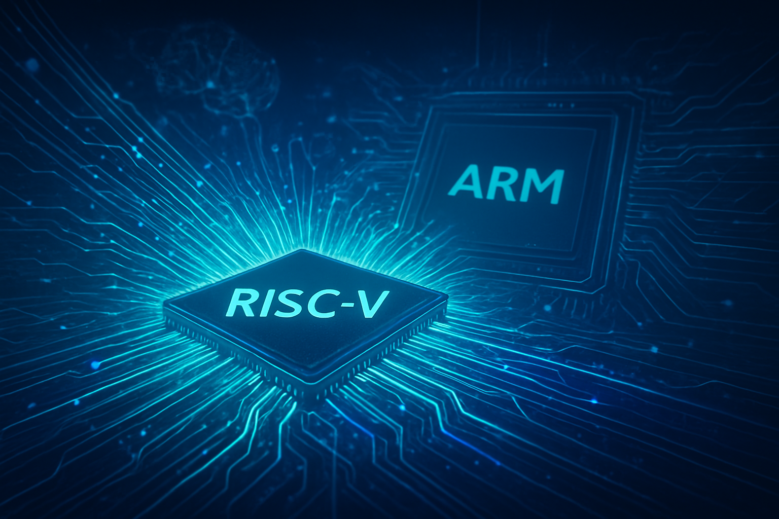
    Unpacking the Silicon War: China's Technical Leap and DUV Ingenuity

    China's domestic chip fabrication initiatives are multifaceted, targeting both mature process nodes and aspiring to advanced AI chip capabilities. The nation's largest contract chipmaker, Semiconductor Manufacturing International Corporation (SMIC), stands at the forefront of this effort. SMIC has notably achieved mass production of 7nm chips, as evidenced by teardowns of Huawei's Kirin 9000s and Kirin 9010 processors found in its Mate 60 and Pura 70 series smartphones. These 7nm chips, often referred to as N+2 process technology, demonstrate China's remarkable progress despite being restricted from accessing cutting-edge Extreme Ultraviolet (EUV) lithography machines.

    Further pushing the boundaries, recent analyses suggest SMIC is advancing towards a 5nm-class node (N+3 process) for Huawei's Kirin 9030 application processor. This is reportedly being achieved through Deep Ultraviolet (DUV) lithography combined with sophisticated multi-patterning techniques like self-aligned quadruple patterning (SAQP), aiming to approach the performance of Nvidia's H100 chip, delivering just under 800 teraflops (FP16). While technically challenging and potentially more expensive with lower yields compared to EUV-based processes, this approach showcases China's ingenuity in overcoming equipment limitations and signals a defiant stance against export controls.

    In the realm of AI chips, Chinese firms are aggressively developing alternatives to Nvidia's (NASDAQ: NVDA) dominant GPUs. Huawei's Ascend series, Alibaba's (NYSE: BABA) inference chips, Cambricon's Siyuan 590, and Baidu's (NASDAQ: BIDU) Kunlun series are all vying for market share. Huawei's Ascend 910B, for instance, has shown performance comparable to Nvidia's A100 in some training tasks. Chinese firms are also exploring innovative architectural designs, such as combining mature 14nm logic chips with 18nm DRAM using 3D hybrid bonding and "software-defined near-memory computing," aiming to achieve high performance without necessarily matching the most advanced logic process nodes.

    This strategic shift represents a fundamental departure from China's previous reliance on global supply chains. The "Big Fund" (China Integrated Circuit Industry Investment Fund) and other state-backed initiatives provide massive funding and policy support, creating a dual focus on both advanced AI chips and a significant ramp-up in mature-node production. Initial reactions from the AI research community and industry experts have ranged from "astonishment" at China's rapid progress, with some describing it as a "Sputnik moment," to cautious skepticism regarding the commercial viability of DUV-based advanced nodes due to higher costs and lower yields. Nvidia CEO Jensen Huang himself has acknowledged China is "nanoseconds behind" in chip development, underscoring the rapid pace of advancement.

    Reshaping the Tech Landscape: Winners, Losers, and Strategic Shifts

    China's monumental investment in domestic chip fabrication and its fierce competition with US firms like Nvidia (NASDAQ: NVDA) are profoundly reshaping the global artificial intelligence and technology landscape, creating distinct beneficiaries and competitive pressures.

    On the Chinese side, domestic chipmakers and AI hardware developers are the primary beneficiaries. Companies like Huawei, with its Ascend series, Cambricon (Siyuan 590), and SMIC (Semiconductor Manufacturing International Corporation) are receiving massive government support, including subsidies and preferential policies. Chinese tech giants such as ByteDance, Alibaba (NYSE: BABA), and Tencent (HKG: 0700), major consumers of AI chips for their data centers, are increasingly switching to domestic semiconductor alternatives, benefiting from subsidized power and a national push for homegrown solutions. This environment also fosters a vibrant domestic AI startup ecosystem, encouraging local innovation and providing opportunities for emerging players like MetaX.

    For US and international tech giants, the landscape is more complex. While Nvidia's dominance in AI training chips and its robust software ecosystem (CUDA) remain crucial for companies like Microsoft (NASDAQ: MSFT), Meta Platforms (NASDAQ: META), and Alphabet (NASDAQ: GOOGL), the loss of the Chinese market for advanced chips represents a significant revenue risk. Nvidia's market share for advanced AI chips in China has plummeted, forcing the company to navigate evolving regulations. The recent conditional approval for Nvidia to sell its H200 AI chips to certain Chinese customers, albeit with a 25% revenue share for the US government, highlights the intricate balance between corporate interests and national security. This situation reinforces the need for US firms to diversify markets and potentially invest more in R&D to maintain their lead outside China. Taiwan Semiconductor Manufacturing Company (TSMC) (NYSE: TSM), a critical global foundry, faces both risks from geopolitical tensions and China's self-sufficiency drive, but also benefits from the overall demand for advanced chips and US efforts to onshore chip production.

    The potential disruption to existing products and services is significant. Products like Nvidia's H100 and newer Blackwell/Rubin architectures are effectively unavailable in China, forcing Chinese companies to adapt their AI model training and deployment strategies. This could lead to a divergence in the underlying hardware architecture supporting AI development in China versus the rest of the world. Moreover, China's massive build-out of legacy chip production capacity could disrupt global supply chains, potentially leading to Chinese dominance in this market segment and affecting industries like automotive.

    Strategically, China gains advantages from massive state subsidies, a large domestic market for economies of scale, and heavy investment in talent and R&D. Its projected dominance in the legacy chip market by 2030 could give it significant influence over global supply chains. The US, meanwhile, maintains a technological lead in cutting-edge AI chip design and advanced manufacturing equipment, leveraging export controls to preserve its advantage. Both nations are engaged in a strategic competition that is fragmenting the global semiconductor market into distinct ecosystems, transforming AI into a critical geoeconomic battlefield.

    A New Cold War? Geopolitical Earthquakes in the AI Landscape

    The wider significance of China's $70 billion investment and its intensifying chip rivalry with the US extends far beyond economic competition, ushering in a new era of geopolitical and technological fragmentation. This strategic push is deeply embedded in China's "Made in China 2025" initiative, aiming for semiconductor self-sufficiency and fundamentally altering the global balance of power.

    This chip race is central to the broader AI landscape, as advanced semiconductors are the "cornerstone for AI development." The competition is accelerating innovation, with both nations pouring resources into AI and related fields. Despite US restrictions on advanced chips, Chinese AI models are rapidly closing the performance gap with their Western counterparts, achieved through building larger compute clusters, optimizing efficiency, and leveraging a robust open-source AI ecosystem. The demand for advanced semiconductors is only set to skyrocket with the global deployment of AI, IoT, and 5G, further intensifying the battle for leadership.

    The geopolitical and economic impacts are profound, leading to an unprecedented restructuring of global supply chains. This fosters a "bifurcated market" where geopolitical alignment becomes a critical factor for companies' survival. "Friend-shoring" strategies are accelerating, with manufacturing shifting to US-allied nations. China's pursuit of self-sufficiency could destabilize the global economy, particularly affecting export-dependent economies like Taiwan. The US CHIPS and Science Act, a significant investment in domestic chip production, directly aims to counteract China's efforts and prevent companies receiving federal funds from increasing advanced processor production in China for 10 years.

    Key concerns revolve around escalating supply chain fragmentation and technological decoupling. The US strategy, often termed "small yard, high fence," aims to restrict critical technologies with military applications while allowing broader economic exchanges. This has pushed the global semiconductor industry into two distinct ecosystems: US-led and Chinese-led. Such bifurcation forces companies to choose sides or diversify, leading to higher costs and operational complexities. Technological decoupling, in its strongest form, suggests a total technological divorce, a prospect fraught with risks, as both nations view control over advanced chips as a national security imperative due to their "dual-use" nature for civilian and military applications.

    This US-China AI chip race is frequently likened to the Cold War-era space race, underscoring its strategic importance. While OpenAI's ChatGPT initially caught China off guard in late 2022, Beijing's rapid advancements in AI models, despite chip restrictions, demonstrate a resilient drive. The dramatic increase in computing power required for training advanced AI models highlights that access to and indigenous production of cutting-edge chips are more critical than ever, making this current technological contest a defining moment in AI's evolution.

    The Road Ahead: Forecasts and Frontiers in the Chip Race

    The geopolitical chip race between China and the United States, particularly concerning firms like Nvidia (NASDAQ: NVDA), is set for dynamic near-term and long-term developments that will shape the future of AI and global technology.

    In the near term, China is expected to continue its aggressive ramp-up of mature-node semiconductor manufacturing capacity. This focus on 28nm and larger chips, critical for industries ranging from automotive to consumer electronics, will see new fabrication plants emerge, further reducing reliance on imports for these foundational components. Companies like SMIC, ChangXin Memory Technologies (CXMT), and Hua Hong Semiconductor will be central to this expansion. While China aims for 70% semiconductor self-sufficiency by 2025, it is likely to fall short, hovering closer to 40%. However, rapid advances in chip assembly and packaging are expected to enhance the performance of older process nodes, albeit with potential challenges in heat output and manufacturing yield.

    Long-term, China's strategy under its 14th Five-Year Plan and subsequent initiatives emphasizes complete technological self-sufficiency, with some targets aiming for 100% import substitution by 2030. The recent launch of "Big Fund III" with over $47 billion underscores this commitment. Beyond mature nodes, China will prioritize advanced chip technologies for AI and disruptive emerging areas like chiplets. Huawei, for instance, is working on multi-year roadmaps for advanced AI chips, targeting petaflop levels in low-precision formats.

    The competition with US firms like Nvidia will remain fierce. US export controls have spurred Chinese tech giants such as Alibaba (NYSE: BABA), Huawei, Baidu (NASDAQ: BIDU), and Cambricon to accelerate proprietary AI chip development. Huawei's Ascend series has emerged as a leading domestic alternative, with some Chinese AI startups demonstrating the ability to train AI models using fewer high-end chips. Recent US policy shifts, allowing Nvidia to export its H200 AI chips to China under conditions including a 25% revenue share for the US government, are seen as a calibrated strategy to slow China's indigenous AI development by creating dependencies on US technology.

    Potential applications and use cases for China's domestically produced chips are vast, spanning artificial intelligence (training generative AI models, smart cities, fintech), cloud computing (Huawei's Kunpeng series), IoT, electric vehicles (EVs), high-performance computing (HPC), data centers, and national security. Semiconductors are inherently dual-use, meaning advanced chips can power commercial AI systems, military intelligence platforms, or encrypted communication networks, aligning with China's military-civil fusion strategy.

    Challenges abound for both sides. China faces persistent technological gaps in advanced EDA software and lithography equipment, talent shortages, and the inherent complexity and cost of cutting-edge manufacturing. The US, conversely, risks accelerating Chinese self-sufficiency through overly stringent export controls, faces potential loss of market share and revenue for its firms, and must continuously innovate to maintain its technological lead. Expert predictions foresee continued bifurcation of semiconductor ecosystems, with China making significant progress in AI despite hardware lags, and a strategic export policy from the US attempting to balance revenue with technological control. The aggressive expansion in mature-node production by China could lead to global oversupply and price dumping.

    The Dawn of a Fragmented Future: A Comprehensive Wrap-up

    China's reported $70 billion investment in domestic chip fabrication, building upon prior massive state-backed funds, is not merely an economic initiative but a profound strategic declaration. It underscores Beijing's unwavering commitment to achieving semiconductor self-sufficiency by 2025 and even 2030, a direct response to escalating US export controls and a bid to secure its technological destiny. This monumental effort has catalyzed a rapid expansion of domestic chip output, particularly in essential mature-node semiconductors, and is actively reshaping global supply chains.

    This escalating competition for chip fabrication dominance marks a pivotal moment in AI history. The nation that controls advanced chip technology will largely dictate the future trajectory of AI development and its applications. Advanced chips are the fundamental building blocks for training increasingly complex AI models, including the large language models that are at the forefront of innovation. The strategic interplay between US policies and China's relentless drive for independence is creating a new, more fragmented equilibrium in the AI semiconductor landscape. US sanctions, while initially disrupting China's high-end chip production, have inadvertently accelerated domestic innovation and investment within China, creating a double-edged sword for American policymakers.

    In the long term, China's consistent investment and innovation are highly likely to cultivate an increasingly self-sufficient domestic chip ecosystem, especially in mature semiconductor nodes. This trajectory points towards a more fragmented global technology landscape and a "multipolar world" in technological innovation. However, the "innovation hard wall" posed by the lack of access to advanced EUV lithography equipment remains China's most significant hurdle for truly cutting-edge chip production. The recent US decision to allow Nvidia (NASDAQ: NVDA) to sell its H200 AI chips to China, while offering short-term economic benefits to US firms, risks creating long-term strategic vulnerabilities by potentially accelerating China's AI and military capabilities. China's vast domestic market is large enough to achieve globally relevant economies of scale, irrespective of export market access, further bolstering its long-term prospects for self-reliance.

    As we look to the coming weeks and months, several critical developments warrant close observation. The implementation of H200 sales to China and Beijing's policy response—whether to restrict or encourage their procurement—will be crucial. The continued progress of Chinese AI chipmakers like Huawei (Ascend series) and Cambricon in closing the performance gap with US counterparts will be a key indicator. Any credible reports on Chinese lithography development beyond the 28nm node, further US policy adjustments, and the investment patterns of major Chinese tech giants like Alibaba (NYSE: BABA) and Tencent (HKG: 0700) will provide further insights into this evolving geopolitical and technological contest. Finally, unexpected breakthroughs in China's ability to achieve advanced chip production using unconventional methods, as seen with the Huawei Mate 60's 7nm chip, will continue to surprise and reshape the narrative. The global tech industry is entering a new era defined by strategic competition and technological nationalism.


    This content is intended for informational purposes only and represents analysis of current AI developments.

    TokenRing AI delivers enterprise-grade solutions for multi-agent AI workflow orchestration, AI-powered development tools, and seamless remote collaboration platforms.
    For more information, visit https://www.tokenring.ai/.

  • AI Transforms Chip Manufacturing: Siemens and GlobalFoundries Forge Future of Semiconductor Production

    AI Transforms Chip Manufacturing: Siemens and GlobalFoundries Forge Future of Semiconductor Production

    December 12, 2025 – In a landmark announcement set to redefine the landscape of semiconductor manufacturing, industrial powerhouse Siemens (ETR: SIE) and leading specialty foundry GlobalFoundries (NASDAQ: GF) have unveiled a significant expansion of their strategic partnership. This collaboration, revealed on December 11-12, 2025, is poised to integrate advanced Artificial Intelligence (AI) into the very fabric of chip design and production, promising unprecedented levels of efficiency, reliability, and supply chain resilience. The move signals a critical leap forward in leveraging AI not just for software, but for the intricate physical processes that underpin the modern digital world.

    This expanded alliance is more than just a business agreement; it's a strategic imperative to address the surging global demand for essential semiconductors, particularly those powering the rapidly evolving fields of AI, autonomous systems, defense, energy, and connectivity. By embedding AI directly into fab tools and operational workflows, Siemens and GlobalFoundries aim to accelerate the development and manufacturing of specialized solutions, bolster regional chip independence, and ensure a more robust and predictable supply chain for the increasingly complex chips vital to national leadership in AI and advanced technologies.

    AI's Deep Integration: A New Era for Fab Automation

    The core of this transformative partnership lies in the deep integration of AI-driven technologies across every stage of semiconductor manufacturing. Siemens is bringing its extensive suite of industrial automation, energy, and building digitalization technologies, including advanced software for chip design, manufacturing, and product lifecycle management. GlobalFoundries, in turn, contributes its specialized process technology and design expertise, notably from its MIPS company, a leader in RISC-V processor IP, crucial for accelerating tailored semiconductor solutions. Together, they envision fabs operating on a foundation of AI-enabled software, real-time sensor feedback, robotics, and predictive maintenance, all cohesively integrated to eliminate manufacturing fragility and ensure continuous operation.

    This collaboration is set to deploy advanced AI-enabled software, sensors, and real-time control systems directly within fab automation environments. Key technical capabilities include centralized AI-enabled automation, predictive maintenance, and the extensive use of digital twins to simulate and optimize manufacturing processes. This approach is designed to enhance equipment uptime, improve operational efficiency, and significantly boost yield reliability—a critical factor for high-performance computing (HPC) and AI workloads where even minor variations can impact chip performance. Furthermore, AI-guided energy systems are being implemented to align with HPC sustainability goals, lowering production costs and reducing the carbon footprint of chip fabrication.

    Historically, semiconductor manufacturing has relied on highly optimized, but largely static, automation and control systems. While advanced, these systems often react to issues rather than proactively preventing them. The Siemens-GlobalFoundries partnership represents a significant departure by embedding proactive, learning AI systems that can predict failures, optimize processes in real-time, and even self-correct. This shift from reactive to predictive and prescriptive manufacturing, driven by AI and digital twins, promises to reduce variability, minimize delays, and provide unprecedented control over complex production lines. Initial reactions from the AI research community and industry experts are overwhelmingly positive, highlighting the potential for these AI integrations to drastically cut costs, accelerate time-to-market, and overcome the physical limitations of traditional manufacturing.

    Reshaping the Competitive Landscape: Winners and Disruptors

    This expanded partnership has profound implications for AI companies, tech giants, and startups across the globe. Siemens (ETR: SIE) and GlobalFoundries (NASDAQ: GF) themselves stand to be major beneficiaries, solidifying their positions at the forefront of industrial automation and specialty chip manufacturing, respectively. Siemens' comprehensive digitalization portfolio, now deeply integrated with GF's fabrication expertise, creates a powerful, end-to-end solution that could become a de facto standard for future smart fabs. GlobalFoundries gains a significant strategic advantage by offering enhanced reliability, efficiency, and sustainability to its customers, particularly those in the high-growth AI and automotive sectors.

    The competitive implications for other major AI labs and tech companies are substantial. Companies heavily reliant on custom or specialized semiconductors will benefit from more reliable and efficient production. However, competing industrial automation providers and other foundries that do not adopt similar AI-driven strategies may find themselves at a disadvantage, struggling to match the efficiency, yield, and speed offered by the Siemens-GF model. This partnership could disrupt existing products and services by setting a new benchmark for semiconductor manufacturing excellence, potentially accelerating the obsolescence of less integrated or AI-deficient fab management systems. From a market positioning perspective, this alliance strategically positions both companies to capitalize on the increasing demand for localized and resilient semiconductor supply chains, especially in regions like the US and Europe, which are striving for greater chip independence.

    A Wider Significance: Beyond the Fab Floor

    This collaboration fits seamlessly into the broader AI landscape, signaling a critical trend: the maturation of AI from theoretical models to practical, industrial-scale applications. It underscores the growing recognition that AI's transformative power extends beyond data centers and consumer applications, reaching into the foundational industries that power our digital world. The impacts are far-reaching, promising not only economic benefits through increased efficiency and reduced costs but also geopolitical advantages by strengthening regional semiconductor supply chains and fostering national leadership in AI.

    The partnership also addresses critical sustainability concerns by leveraging AI-guided energy systems in fabs, aligning with global efforts to reduce the carbon footprint of energy-intensive industries. Potential concerns, however, include the complexity of integrating such advanced AI systems into legacy infrastructure, the need for a highly skilled workforce to manage these new technologies, and potential cybersecurity vulnerabilities inherent in highly interconnected systems. When compared to previous AI milestones, such as the breakthroughs in natural language processing or computer vision, this development represents a crucial step in AI's journey into the physical world, demonstrating its capacity to optimize complex industrial processes rather than just intellectual tasks. It signifies a move towards truly intelligent manufacturing, where AI acts as a central nervous system for production.

    The Horizon of Intelligent Manufacturing: What Comes Next

    Looking ahead, the expanded Siemens-GlobalFoundries partnership foreshadows a future of increasingly autonomous and intelligent semiconductor manufacturing. Near-term developments are expected to focus on the full deployment and optimization of the AI-driven predictive maintenance and digital twin technologies across GF's fabs, leading to measurable improvements in uptime and yield. In the long term, experts predict the emergence of fully autonomous fabs, where AI not only monitors and optimizes but also independently manages production schedules, identifies and resolves issues, and even adapts to new product designs with minimal human intervention.

    Potential applications and use cases on the horizon include the rapid prototyping and mass production of highly specialized AI accelerators and neuromorphic chips, designed to power the next generation of AI systems. The integration of AI throughout the design-to-manufacturing pipeline could also lead to "self-optimizing" chips, where design parameters are dynamically adjusted based on real-time manufacturing feedback. Challenges that need to be addressed include the development of robust AI safety protocols, standardization of AI integration interfaces across different equipment vendors, and addressing the significant data privacy and security implications of such interconnected systems. Experts predict that this partnership will serve as a blueprint for other industrial sectors, driving a broader adoption of AI-enabled industrial automation and setting the stage for a new era of smart manufacturing globally.

    A Defining Moment for AI in Industry

    In summary, the expanded partnership between Siemens and GlobalFoundries represents a defining moment for the application of AI in industrial settings, particularly within the critical semiconductor sector. The key takeaways are the strategic integration of AI for predictive maintenance, operational optimization, and enhanced supply chain resilience, coupled with a strong focus on sustainability and regional independence. This development's significance in AI history cannot be overstated; it marks a pivotal transition from theoretical AI capabilities to tangible, real-world impact on the foundational industry of the digital age.

    The long-term impact is expected to be a more efficient, resilient, and sustainable global semiconductor ecosystem, capable of meeting the escalating demands of an AI-driven future. What to watch for in the coming weeks and months are the initial deployment results from GlobalFoundries' fabs, further announcements regarding specific AI-powered tools and features, and how competing foundries and industrial automation firms respond to this new benchmark. This collaboration is not just about making chips faster; it's about fundamentally rethinking how the world makes chips, with AI at its intelligent core.


    This content is intended for informational purposes only and represents analysis of current AI developments.

    TokenRing AI delivers enterprise-grade solutions for multi-agent AI workflow orchestration, AI-powered development tools, and seamless remote collaboration platforms.
    For more information, visit https://www.tokenring.ai/.

  • The AI Infrastructure Arms Race: Specialized Data Centers Become the New Frontier

    The AI Infrastructure Arms Race: Specialized Data Centers Become the New Frontier

    The relentless pursuit of artificial intelligence (AI) advancements is igniting an unprecedented demand for a new breed of digital infrastructure: specialized AI data centers. These facilities, purpose-built to handle the immense computational and energy requirements of modern AI workloads, are rapidly becoming the bedrock of the AI revolution. From training colossal language models to powering real-time analytics, traditional data centers are proving increasingly inadequate, paving the way for a global surge in investment and development. A prime example of this critical infrastructure shift is the proposed $300 million AI data center in Lewiston, Maine, a project emblematic of the industry's pivot towards dedicated AI compute power.

    This monumental investment in Lewiston, set to redevelop the historic Bates Mill No. 3, underscores a broader trend where cities and regions are vying to become hubs for the next generation of industrial powerhouses – those fueled by artificial intelligence. The project, spearheaded by MillCompute, aims to transform the vacant mill into a Tier III AI data center, signifying a commitment to high availability and continuous operation crucial for demanding AI tasks. As AI continues to permeate every facet of technology and business, the race to build and operate these specialized computational fortresses is intensifying, signaling a fundamental reshaping of the digital landscape.

    Engineering the Future: The Technical Demands of AI Data Centers

    The technical specifications and capabilities of specialized AI data centers mark a significant departure from their conventional predecessors. The core difference lies in the sheer computational intensity and the unique hardware required for AI workloads, particularly for deep learning and machine learning model training. Unlike general-purpose servers, AI systems heavily rely on specialized accelerators such as Graphics Processing Units (GPUs) and Tensor Processing Units (TPUs), which are optimized for parallel processing and capable of performing millions of computations per second. This demand for powerful hardware is pushing rack densities from a typical 5-15kW to an astonishing 50-100kW+, with some cutting-edge designs even reaching 250kW per rack.

    Such extreme power densities bring with them unprecedented challenges, primarily in energy consumption and thermal management. Traditional air-cooling systems, once the standard, are often insufficient to dissipate the immense heat generated by these high-performance components. Consequently, AI data centers are rapidly adopting advanced liquid cooling solutions, including direct-to-chip and immersion cooling, which can reduce energy requirements for cooling by up to 95% while simultaneously enhancing performance and extending hardware lifespan. Furthermore, the rapid exchange of vast datasets inherent in AI operations necessitates robust network infrastructure, featuring high-speed, low-latency, and high-bandwidth fiber optic connectivity to ensure seamless communication between thousands of processors.

    The global AI data center market reflects this technical imperative, projected to explode from $236.44 billion in 2025 to $933.76 billion by 2030, at a compound annual growth rate (CAGR) of 31.6%. This exponential growth highlights how current infrastructure is simply not designed to efficiently handle the petabytes of data and complex algorithms that define modern AI. The shift is not merely an upgrade but a fundamental redesign, prioritizing power availability, advanced cooling, and optimized network architectures to unlock the full potential of AI.

    Reshaping the AI Ecosystem: Impact on Companies and Competitive Dynamics

    The proliferation of specialized AI data centers has profound implications for AI companies, tech giants, and startups alike, fundamentally reshaping the competitive landscape. Hyperscalers and cloud computing providers, such as Amazon (NASDAQ: AMZN), Microsoft (NASDAQ: MSFT), Google (NASDAQ: GOOGL), and Meta (NASDAQ: META), are at the forefront of this investment wave, pouring billions into building next-generation AI-optimized infrastructure. These companies stand to benefit immensely by offering scalable, high-performance AI compute resources to a vast customer base, cementing their market positioning as essential enablers of AI innovation.

    For major AI labs and tech companies, access to these specialized data centers is not merely an advantage but a necessity for staying competitive. The ability to quickly train larger, more complex models, conduct extensive research, and deploy sophisticated AI services hinges on having robust, dedicated infrastructure. Companies without direct access or significant investment in such facilities may find themselves at a disadvantage in the race to develop and deploy cutting-edge AI. This development could lead to a further consolidation of power among those with the capital and foresight to invest heavily in AI infrastructure, potentially creating barriers to entry for smaller startups.

    However, specialized AI data centers also create new opportunities. Companies like MillCompute, focusing on developing and operating these facilities, are emerging as critical players in the AI supply chain. Furthermore, the demand for specialized hardware, advanced cooling systems, and energy solutions fuels innovation and growth for manufacturers and service providers in these niche areas. The market is witnessing a strategic realignment where the physical infrastructure supporting AI is becoming as critical as the algorithms themselves, driving new partnerships, acquisitions, and a renewed focus on strategic geographical placement for optimal power and cooling.

    The Broader AI Landscape: Impacts, Concerns, and Milestones

    The increasing demand for specialized AI data centers fits squarely into the broader AI landscape as a critical trend shaping the future of technology. It underscores that the AI revolution is not just about algorithms and software, but equally about the underlying physical infrastructure that makes it possible. This infrastructure boom is driving a projected 165% increase in global data center power demand by 2030, primarily fueled by AI workloads, necessitating a complete rethinking of how digital infrastructure is designed, powered, and operated.

    The impacts are wide-ranging, from economic development in regions hosting these facilities, like Lewiston, to significant environmental concerns. The immense energy consumption of AI data centers raises questions about sustainability and carbon footprint. This has spurred a strong push towards renewable energy integration, including on-site generation, battery storage, and hybrid power systems, as companies strive to meet corporate sustainability commitments and mitigate environmental impact. Site selection is increasingly prioritizing energy availability and access to green power sources over traditional factors.

    This era of AI infrastructure build-out can be compared to previous technological milestones, such as the dot-com boom that drove the construction of early internet data centers or the expansion of cloud infrastructure in the 2010s. However, the current scale and intensity of demand, driven by the unique computational requirements of AI, are arguably unprecedented. Potential concerns beyond energy consumption include the concentration of AI power in the hands of a few major players, the security of these critical facilities, and the ethical implications of the AI systems they support. Nevertheless, the investment in specialized AI data centers is a clear signal that the world is gearing up for a future where AI is not just an application, but the very fabric of our digital existence.

    The Road Ahead: Future Developments and Expert Predictions

    Looking ahead, the trajectory of specialized AI data centers points towards several key developments. Near-term, we can expect a continued acceleration in the adoption of advanced liquid cooling technologies, moving from niche solutions to industry standards as rack densities continue to climb. There will also be an increased focus on AI-optimized facility design, with data centers being built from the ground up to accommodate high-performance GPUs, NVMe SSDs for ultra-fast storage, and high-speed networking like InfiniBand. Experts predict that the global data center infrastructure market, fueled by the AI arms race, will surpass $1 trillion in annual spending by 2030.

    Long-term, the integration of edge computing with AI is poised to gain significant traction. As AI applications demand lower latency and real-time processing, compute resources will increasingly be pushed closer to end-users and data sources. This will likely lead to the development of smaller, distributed AI-specific data centers at the edge, complementing the hyperscale facilities. Furthermore, research into more energy-efficient AI hardware and algorithms will become paramount, alongside innovations in heat reuse technologies, where waste heat from data centers could be repurposed for district heating or other industrial processes.

    Challenges that need to be addressed include securing reliable and abundant clean energy sources, managing the complex supply chains for specialized hardware, and developing skilled workforces to operate and maintain these advanced facilities. Experts predict a continued strategic global land grab for sites with robust power grids, access to renewable energy, and favorable climates for natural cooling. The evolution of specialized AI data centers will not only shape the capabilities of AI itself but also influence energy policy, urban planning, and environmental sustainability for decades to come.

    A New Foundation for the AI Age

    The emergence and rapid expansion of specialized data centers to support AI computations represent a pivotal moment in the history of artificial intelligence. Projects like the $300 million AI data center in Lewiston are not merely construction endeavors; they are the foundational keystones for the next era of technological advancement. The key takeaway is clear: the future of AI is inextricably linked to the development of purpose-built, highly efficient, and incredibly powerful infrastructure designed to meet its unique demands.

    This development signifies AI's transition from a nascent technology to a mature, infrastructure-intensive industry. Its significance in AI history is comparable to the invention of the microchip or the widespread adoption of the internet, as it provides the essential physical layer upon which all future AI breakthroughs will be built. The long-term impact will be a world increasingly powered by intelligent systems, with access to unprecedented computational power enabling solutions to some of humanity's most complex challenges.

    In the coming weeks and months, watch for continued announcements of new AI data center projects, further advancements in cooling and power management technologies, and intensified competition among cloud providers to offer the most robust AI compute services. The race to build the ultimate AI infrastructure is on, and its outcome will define the capabilities and trajectory of artificial intelligence for generations.


    This content is intended for informational purposes only and represents analysis of current AI developments.

    TokenRing AI delivers enterprise-grade solutions for multi-agent AI workflow orchestration, AI-powered development tools, and seamless remote collaboration platforms.
    For more information, visit https://www.tokenring.ai/.

  • NASA JPL Unveils AI-Powered Rover Operations Center, Ushering in a New Era of Autonomous Space Exploration

    NASA JPL Unveils AI-Powered Rover Operations Center, Ushering in a New Era of Autonomous Space Exploration

    PASADENA, CA – December 11, 2025 – The NASA Jet Propulsion Laboratory (JPL) has officially launched its new Rover Operations Center (ROC), marking a pivotal moment in the quest for advanced autonomous space exploration. This state-of-the-art facility is poised to revolutionize how future lunar and Mars missions are conducted, with an aggressive focus on accelerating AI-enabled autonomy. The ROC aims to integrate decades of JPL's unparalleled experience in rover operations with cutting-edge artificial intelligence capabilities, setting a new standard for mission efficiency and scientific discovery.

    The immediate significance of the ROC lies in its ambition to be a central hub for developing and deploying AI solutions that empower rovers to operate with unprecedented independence. By applying AI to critical operational workflows, such as route planning and scientific target selection, the center is designed to enhance mission productivity and enable more complex exploratory endeavors. This initiative is not merely an incremental upgrade but a strategic leap towards a future where robotic explorers can make real-time, intelligent decisions on distant celestial bodies, drastically reducing the need for constant human oversight and unlocking new frontiers in space science.

    AI Takes the Helm: Technical Advancements in Rover Autonomy

    The Rover Operations Center (ROC) represents a significant technical evolution in space robotics, building upon JPL's storied history of developing autonomous systems. At its core, the ROC is focused on integrating and advancing several key AI capabilities to enhance rover autonomy. One immediate application is the use of generative AI for sophisticated route planning, a capability already being leveraged by the Perseverance rover team on Mars. This moves beyond traditional pre-programmed paths, allowing rovers to dynamically assess terrain, identify hazards, and plot optimal routes in real-time, significantly boosting efficiency and safety.

    Technically, the ROC is developing a suite of advanced solutions, including engineering foundation models that can learn from vast datasets of mission telemetry and environmental data, digital twins for high-fidelity simulation and testing, and AI models specifically adapted for the unique challenges of space environments. A major focus is on edge AI-augmented autonomy stack solutions, enabling rovers to process data and make decisions onboard without constant communication with Earth, which is crucial given the communication delays over interplanetary distances. This differs fundamentally from previous approaches where autonomy was more rule-based and reactive; the new AI-driven systems are designed to be proactive, adaptive, and capable of learning from their experiences. Initial reactions from the AI research community and industry experts have been overwhelmingly positive, highlighting the ROC's potential to bridge the gap between theoretical AI advancements and practical, mission-critical applications in extreme environments. Experts laud the integration of multi-robot autonomy, as demonstrated by the Cooperative Autonomous Distributed Robotic Exploration (CADRE) technology demonstration, which involves teams of small, collaborative rovers. This represents a paradigm shift from single-robot operations to coordinated, intelligent swarms, dramatically expanding exploration capabilities.

    The center also provides comprehensive support for missions, encompassing systems engineering, integration, and testing (SEIT), dedicated teams for onboard autonomy/AI development, advanced planning and scheduling tools for orbital and interplanetary communications, and robust capabilities for critical anomaly response. This holistic approach ensures that AI advancements are not just theoretical but are rigorously tested and seamlessly integrated into all facets of mission operations. The emphasis on AI-assisted operations automation aims to reduce human workload and error, allowing mission controllers to focus on higher-level strategic decisions rather than granular operational details.

    Reshaping the Landscape: Impact on AI Companies and Tech Giants

    The establishment of NASA JPL's (NASDAQ: LMT) (NYSE: BA) (NYSE: RTX) new Rover Operations Center and its aggressive push for AI-enabled autonomy will undoubtedly send ripples across the AI industry, benefiting a diverse range of companies from established tech giants to agile startups. Companies specializing in machine learning frameworks, computer vision, robotics, and advanced simulation technologies stand to gain significantly. Firms like NVIDIA (NASDAQ: NVDA), known for its powerful GPUs and AI platforms, could see increased demand for hardware and software solutions capable of handling the intensive computational requirements of onboard AI for space applications. Similarly, companies developing robust AI safety and reliability tools will become critical partners in ensuring the flawless operation of autonomous systems in high-stakes space missions.

    The competitive implications for major AI labs and tech companies are substantial. Those with a strong focus on reinforcement learning, generative AI, and multi-agent systems will find themselves in a prime position to collaborate with JPL or develop parallel technologies for commercial space ventures. The expertise gained from developing AI for the extreme conditions of space—where data is scarce, computational resources are limited, and failure is not an option—could lead to breakthroughs applicable across various terrestrial industries, from autonomous vehicles to industrial automation. This could disrupt existing products or services by setting new benchmarks for AI robustness and adaptability.

    Market positioning and strategic advantages will favor companies that can demonstrate proven capabilities in developing resilient, low-power AI solutions suitable for edge computing in harsh environments. Startups specializing in novel sensor fusion techniques, advanced path planning algorithms, or innovative human-AI collaboration interfaces for mission control could find lucrative niches. Furthermore, the ROC's emphasis on technology transfer and strategic partnerships with industry and academia signals a collaborative ecosystem where smaller, specialized AI firms can contribute their unique expertise and potentially scale their innovations through NASA's rigorous validation process, gaining invaluable credibility and market traction. The demand for AI solutions that can handle partial observability, long-term planning, and dynamic adaptation in unknown environments will drive innovation and investment across the AI sector.

    A New Frontier: Wider Significance in the AI Landscape

    The launch of NASA JPL's Rover Operations Center and its dedication to accelerating AI-enabled autonomy for space exploration represents a monumental stride within the broader AI landscape, signaling a maturation of AI capabilities beyond traditional enterprise applications. This initiative fits perfectly into the growing trend of deploying AI in extreme and unstructured environments, pushing the boundaries of what autonomous systems can achieve. It underscores a significant shift from AI primarily as a data analysis or prediction tool to AI as an active, intelligent agent capable of complex decision-making and problem-solving in real-world (or rather, "space-world") scenarios.

    The impacts are profound, extending beyond the immediate realm of space exploration. By proving AI's reliability and effectiveness in the unforgiving vacuum of space, JPL is effectively validating AI for a host of other critical applications on Earth, such as disaster response, deep-sea exploration, and autonomous infrastructure maintenance. This development accelerates the trust in AI systems for high-stakes operations, potentially influencing regulatory frameworks and public acceptance of advanced autonomy. However, potential concerns also arise, primarily around the ethical implications of increasingly autonomous systems, the challenges of debugging and verifying complex AI behaviors in remote environments, and the need for robust cybersecurity measures to protect these invaluable assets from interference.

    Comparing this to previous AI milestones, the ROC's focus on comprehensive, mission-critical autonomy for space exploration stands alongside breakthroughs like DeepMind's AlphaGo defeating human champions or the rapid advancements in large language models. While those milestones demonstrated AI's cognitive prowess in specific domains, JPL's work showcases AI's ability to perform complex physical tasks, adapt to unforeseen circumstances, and collaborate with human operators in a truly operational setting. It's a testament to AI's evolution from a computational marvel to a practical, indispensable tool for pushing the boundaries of human endeavor. This initiative highlights the critical role of AI in enabling humanity to venture further and more efficiently into the cosmos.

    Charting the Course: Future Developments and Horizons

    The establishment of NASA JPL's Rover Operations Center sets the stage for a cascade of exciting future developments in AI-enabled space exploration. In the near term, we can expect to see an accelerated deployment of advanced AI algorithms on upcoming lunar and Mars missions, particularly for enhanced navigation, scientific data analysis, and intelligent resource management. The CADRE (Cooperative Autonomous Distributed Robotic Exploration) mission, involving a team of small, autonomous rovers, is a prime example of a near-term application, demonstrating multi-robot collaboration and mapping on the lunar surface. This will pave the way for more complex swarms of robots working in concert.

    Long-term developments will likely involve increasingly sophisticated AI systems that can independently plan entire mission segments, adapt to unexpected environmental changes, and even perform on-the-fly repairs or reconfigurations of robotic hardware. Experts predict the emergence of AI-powered "digital twins" of entire planetary surfaces, allowing for highly accurate simulations and predictive modeling of rover movements and scientific outcomes. Potential applications and use cases on the horizon include AI-driven construction of lunar bases, autonomous mining operations on asteroids, and self-replicating robotic explorers capable of sustained, multi-decade missions without direct human intervention. The ROC's efforts to develop engineering foundation models and edge AI-augmented autonomy stack solutions are foundational to these ambitious future endeavors.

    However, significant challenges need to be addressed. These include developing more robust and fault-tolerant AI architectures, ensuring ethical guidelines for autonomous decision-making, and creating intuitive human-AI interfaces that allow astronauts and mission controllers to effectively collaborate with highly intelligent machines. Furthermore, the computational and power constraints inherent in space missions will continue to drive research into highly efficient and miniaturized AI hardware. Experts predict that the next decade will witness AI transitioning from an assistive technology to a truly co-equal partner in space exploration, with systems capable of making critical decisions independently while maintaining transparency and explainability for human oversight. The focus will shift towards creating truly symbiotic relationships between human explorers and their AI counterparts.

    A New Era Dawns: The Enduring Significance of AI in Space

    The unveiling of NASA JPL's Rover Operations Center marks a profound and irreversible shift in the trajectory of space exploration, solidifying AI's role as an indispensable co-pilot for humanity's cosmic ambitions. The key takeaway from this development is the commitment to pushing AI beyond terrestrial applications into the most demanding and unforgiving environments imaginable, proving its mettle in scenarios where failure carries catastrophic consequences. This initiative is not just about building smarter rovers; it's about fundamentally rethinking how we explore, reducing human risk, accelerating discovery, and expanding our reach across the solar system.

    In the annals of AI history, this development will be assessed as a critical turning point, analogous to the first successful deployment of AI in medical diagnostics or autonomous driving. It signifies the transition of advanced AI from theoretical research and controlled environments to real-world, high-stakes operational settings. The long-term impact will be transformative, enabling missions that are currently unimaginable due to constraints in communication, human endurance, or operational complexity. We are witnessing the dawn of an era where robotic explorers, imbued with sophisticated artificial intelligence, will venture further, discover more, and provide insights that will reshape our understanding of the universe.

    In the coming weeks and months, watch for announcements regarding the initial AI-enhanced capabilities deployed on existing or upcoming missions, particularly those involving lunar exploration. Pay close attention to the progress of collaborative robotics projects like CADRE, which will serve as crucial testbeds for multi-agent autonomy. The strategic partnerships JPL forges with industry and academia will also be key indicators of how rapidly these AI advancements will propagate. This is not merely an incremental improvement; it is a foundational shift that will redefine the very nature of space exploration, making it more efficient, more ambitious, and ultimately, more successful.


    This content is intended for informational purposes only and represents analysis of current AI developments.

    TokenRing AI delivers enterprise-grade solutions for multi-agent AI workflow orchestration, AI-powered development tools, and seamless remote collaboration platforms.
    For more information, visit https://www.tokenring.ai/.

  • Universities Forge Future of AI: Wyoming Pioneers Comprehensive, Ethical Integration

    Universities Forge Future of AI: Wyoming Pioneers Comprehensive, Ethical Integration

    LARAMIE, WY – December 11, 2025 – In a landmark move poised to reshape the landscape of artificial intelligence education and application, the University of Wyoming (UW) has officially established its "President's AI Across the University Commission." Launched just yesterday, on December 10, 2025, this pioneering initiative signals a new era where universities are not merely adopting AI, but are strategically embedding it across every facet of academic, research, and administrative life, with a steadfast commitment to ethical implementation. This development places UW at the forefront of a growing global trend, as higher education institutions recognize the urgent need for holistic, interdisciplinary strategies to harness AI's transformative power responsibly.

    The commission’s establishment underscores a critical shift from siloed AI development to a unified, institution-wide approach. Its immediate significance lies in its proactive stance to guide AI policy, foster understanding, and ensure compliant, ethical deployment, preparing students and the state of Wyoming for an an AI-driven future. This comprehensive framework aims to not only integrate AI into diverse disciplines but also to cultivate a workforce equipped with both technical prowess and a deep understanding of AI's societal implications.

    A Blueprint for Integrated AI: UW's Visionary Commission

    The President's AI Across the University Commission is a meticulously designed strategic initiative, building upon UW's existing AI efforts, particularly from the Office of the Provost. Its core mission is to provide leadership in guiding AI policy development, ensuring alignment with the university's strategic priorities, and supporting educators, researchers, and staff in deploying AI best practices. A key deliverable, "UW and AI Today," is slated for completion by June 15, which will outline a strategic framework for UW's AI policy, investments, and best practices for the next two years.

    Comprised of 12 members and chaired by Jeff Hamerlinck, associate director of the School of Computing and President's Fellow, the commission ensures broad representation, including faculty, staff, and students. To facilitate comprehensive integration, it operates with five thematic committees: Teaching and Learning with AI, Academic Hiring regarding AI, AI-related Research and Development Opportunities, AI Services and Tools, and External Collaborations. This structure guarantees that AI's impact on curriculum, faculty recruitment, research, technological infrastructure, and industry partnerships is addressed systematically.

    UW's commitment is further bolstered by substantial financial backing, including $8.75 million in combined private and state funds to boost AI capacity and innovation statewide, alongside a nearly $4 million grant from the National Science Foundation (NSF) for state-of-the-art computing infrastructure. This dedicated funding is crucial for supporting cross-disciplinary projects in areas vital to Wyoming, such as livestock management, wildlife conservation, energy exploration, agriculture, water use, and rural healthcare, demonstrating a practical application of AI to real-world challenges.

    The commission’s approach differs significantly from previous, often fragmented, departmental AI initiatives. By establishing a central, university-wide body with dedicated funding and a clear mandate for ethical integration, UW is moving beyond ad-hoc adoption to a structured, anticipatory model. This holistic strategy aims to foster a comprehensive understanding of AI's impact across the entire university community, preparing the next generation of leaders and innovators not just to use AI, but to shape its responsible evolution.

    Ripple Effects: How University AI Strategies Influence Industry

    The proactive development of comprehensive AI strategies by universities like the University of Wyoming (UW) carries significant implications for AI companies, tech giants (NASDAQ: GOOGL), and startups. By establishing commissions focused on strategic integration and ethical use, universities are cultivating a pipeline of talent uniquely prepared for the complexities of the modern AI landscape. Graduates from programs emphasizing AI literacy and ethics, such as UW's Master's in AI and courses like "Ethics in the Age of Generative AI," will enter the workforce not only with technical skills but also with a critical understanding of fairness, bias, and responsible deployment—qualities increasingly sought after by companies navigating regulatory scrutiny and public trust concerns.

    Moreover, the emphasis on external collaborations within UW's commission and similar initiatives at other universities creates fertile ground for partnerships. AI companies can benefit from direct access to cutting-edge academic research, leveraging university expertise to develop new products, refine existing services, and address complex technical challenges. These collaborations can range from joint research projects and sponsored labs to talent acquisition pipelines and licensing opportunities for university-developed AI innovations. For startups, university partnerships offer a pathway to validation, resources, and early-stage talent, potentially accelerating their growth and market entry.

    The focus on ethical and compliant AI implementation, as explicitly stated in UW's mission, has broader competitive implications. As universities champion responsible AI development, they indirectly influence industry standards. Companies that align with these emerging ethical frameworks—prioritizing transparency, accountability, and user safety—will likely gain a competitive advantage, fostering greater trust with consumers and regulators. Conversely, those that neglect ethical considerations may face reputational damage, legal challenges, and a struggle to attract top talent trained in responsible AI practices. This shift could disrupt existing products or services that have not adequately addressed ethical concerns, pushing companies to re-evaluate their AI development lifecycles and market positioning.

    A Broader Canvas: AI in the Academic Ecosystem

    The University of Wyoming's initiative is not an isolated event but a significant part of a broader, global trend in higher education. Universities worldwide are grappling with the rapid advancement of AI and its profound implications, moving towards institution-wide strategies that mirror UW's comprehensive approach. Institutions like the University of Oxford, with its Institute for Ethics in AI, Stanford University (NYSE: MSFT), with its Institute for Human-Centered Artificial Intelligence (HAI) and RAISE-Health, and Carnegie Mellon University (CMU), with its Responsible AI Initiative, are all establishing dedicated centers and cross-disciplinary programs to integrate AI ethically and effectively.

    This widespread adoption of comprehensive AI strategies signifies a recognition that AI is not just a computational tool but a fundamental force reshaping every discipline, from humanities to healthcare. The impacts are far-reaching: enhancing research capabilities across fields, transforming teaching methodologies, streamlining administrative tasks, and preparing a future workforce for an AI-driven economy. By fostering AI literacy among students and within K-12 schools, as UW aims to do, these initiatives are democratizing access to AI knowledge and empowering communities to thrive in a technology-driven future.

    However, this rapid integration also brings potential concerns. Ensuring equitable access to AI education, mitigating algorithmic bias, protecting data privacy, and navigating the ethical dilemmas posed by increasingly autonomous systems remain critical challenges. Universities are uniquely positioned to address these concerns through dedicated research, policy development, and robust ethical frameworks. Compared to previous AI milestones, where breakthroughs often occurred in isolated labs, the current era is defined by a concerted, institutional effort to integrate AI thoughtfully and responsibly, learning from past oversights and proactively shaping AI's societal impact. This proactive, ethical stance marks a mature phase in AI's evolution within academia.

    The Horizon of AI Integration: What Comes Next

    The establishment of commissions like UW's "President's AI Across the University Commission" heralds a future where AI is seamlessly woven into the fabric of higher education and, consequently, society. In the near term, we can expect to see the fruits of initial strategic frameworks, such as UW's "UW and AI Today" report, guiding immediate investments and policy adjustments. This will likely involve the rollout of new AI-integrated curricula, faculty development programs, and pilot projects leveraging AI in administrative functions. Universities will continue to refine their academic integrity policies to address generative AI, emphasizing disclosure and ethical use.

    Longer-term developments will likely include the proliferation of interdisciplinary AI research hubs, attracting significant federal and private grants to tackle grand societal challenges using AI. We can anticipate the creation of more specialized academic programs, like UW's Master's in AI, designed to produce graduates who can not only develop AI but also critically evaluate its ethical and societal implications across diverse sectors. Furthermore, the emphasis on industry collaboration is expected to deepen, leading to more robust partnerships between universities and companies, accelerating the transfer of academic research into practical applications and fostering innovation ecosystems.

    Challenges that need to be addressed include keeping pace with the rapid evolution of AI technology, securing sustained funding for infrastructure and talent, and continuously refining ethical guidelines to address unforeseen applications and societal impacts. Maintaining a balance between innovation and responsible deployment will be paramount. Experts predict that these university-led initiatives will fundamentally reshape the workforce, creating new job categories and demanding a higher degree of AI literacy across all professions. The next decade will likely see AI become as ubiquitous and foundational to university operations and offerings as the internet is today, with ethical considerations at its core.

    Charting a Responsible Course: The Enduring Impact of University AI Strategies

    The University of Wyoming's "President's AI Across the University Commission," established just yesterday, marks a pivotal moment in the strategic integration of artificial intelligence within higher education. It encapsulates a global trend where universities are moving beyond mere adoption to actively shaping the ethical development and responsible deployment of AI across all disciplines. The key takeaways are clear: a holistic, institution-wide approach is essential for navigating the complexities of AI, ethical considerations must be embedded from the outset, and interdisciplinary collaboration is vital for unlocking AI's full potential for societal benefit.

    This development holds profound significance in AI history, representing a maturation of the academic response to this transformative technology. It signals a shift from reactive adaptation to proactive leadership, positioning universities not just as consumers of AI, but as critical architects of its future—educating the next generation, conducting groundbreaking research, and establishing ethical guardrails. The long-term impact will be a more ethically conscious and skilled AI workforce, innovative solutions to complex global challenges, and a society better equipped to understand and leverage AI responsibly.

    In the coming weeks and months, the academic community and industry stakeholders will be closely watching the outcomes of UW's initial strategic framework, "UW and AI Today," due by June 15. The success and lessons learned from this commission, alongside similar initiatives at leading universities worldwide, will provide invaluable insights into best practices for integrating AI responsibly and effectively. As AI continues its rapid evolution, the foundational work being laid by institutions like the University of Wyoming will be instrumental in ensuring that this powerful technology serves humanity's best interests.


    This content is intended for informational purposes only and represents analysis of current AI developments.

    TokenRing AI delivers enterprise-grade solutions for multi-agent AI workflow orchestration, AI-powered development tools, and seamless remote collaboration platforms.
    For more information, visit https://www.tokenring.ai/.

  • RISC-V Rises: An Open-Source Revolution Poised to Disrupt ARM’s Chip Dominance

    RISC-V Rises: An Open-Source Revolution Poised to Disrupt ARM’s Chip Dominance

    The semiconductor industry is on the cusp of a significant shift as the open-standard RISC-V instruction set architecture (ISA) rapidly gains traction, presenting a formidable challenge to ARM's long-standing dominance in chip design. Developed at the University of California, Berkeley, and governed by the non-profit RISC-V International, this royalty-free and highly customizable architecture is democratizing processor design, fostering unprecedented innovation, and potentially reshaping the competitive landscape for silicon intellectual property. Its modularity, cost-effectiveness, and vendor independence are attracting a growing ecosystem of industry giants and nimble startups alike, heralding a new era where chip design is no longer exclusively the domain of proprietary giants.

    The immediate significance of RISC-V lies in its potential to dramatically lower barriers to entry for chip development, allowing companies to design highly specialized processors without incurring the hefty licensing fees associated with proprietary ISAs like ARM and x86. This open-source ethos is not only driving down costs but also empowering designers with unparalleled flexibility to tailor processors for specific applications, from tiny IoT devices to powerful AI accelerators and data center solutions. As geopolitical tensions highlight the need for independent and secure supply chains, RISC-V's neutral governance further enhances its appeal, positioning it as a strategic alternative for nations and corporations seeking autonomy in their technological infrastructure.

    A Technical Deep Dive into RISC-V's Architecture and AI Prowess

    At its core, RISC-V is a clean-slate, open-standard instruction set architecture (ISA) built upon Reduced Instruction Set Computer (RISC) principles, designed for simplicity, modularity, and extensibility. Unlike proprietary ISAs, its specifications are released under permissive open-source licenses, eliminating royalty payments—a stark contrast to ARM's per-chip royalty model. The architecture features a small, mandatory base integer ISA (RV32I, RV64I, RV128I) for general-purpose computing, which can be augmented by a range of optional standard extensions. These include M for integer multiply/divide, A for atomic operations, F and D for single and double-precision floating-point, C for compressed instructions to reduce code size, and crucially, V for vector operations, which are vital for high-performance computing and AI/ML workloads. This modularity allows chip designers to select only the necessary instruction groups, optimizing for power, performance, and silicon area.

    The true differentiator for RISC-V, particularly in the context of AI, lies in its unparalleled ability for custom extensions. Designers are free to define non-standard, application-specific instructions and accelerators without breaking compliance with the main RISC-V specification. This capability is a game-changer for AI/ML, enabling the direct integration of specialized hardware like Tensor Processing Units (TPUs), Graphics Processing Units (GPUs), or Neural Processing Units (NPUs) into the ISA. This level of customization allows for processors to be precisely tailored for specific AI algorithms, transformer workloads, and large language models (LLMs), offering an optimization potential that ARM's more fixed IP cores cannot match. While ARM has focused on evolving its instruction set over decades, RISC-V's fresh design avoids legacy complexities, promoting a more streamlined and efficient architecture.

    Initial reactions from the AI research community and industry experts have been overwhelmingly positive, recognizing RISC-V as an ideal platform for the future of AI/ML. Its modularity and extensibility are seen as perfectly suited for integrating custom AI accelerators, leading to highly efficient and performant solutions, especially at the edge. Experts note that RISC-V can offer significant advantages in computational performance per watt compared to ARM and x86, making it highly attractive for power-constrained edge AI devices and battery-operated solutions. The open nature of RISC-V also fosters a unified programming model across different processing units (CPU, GPU, NPU), simplifying development and accelerating time-to-market for AI solutions.

    Furthermore, RISC-V is democratizing AI hardware development, lowering the barriers to entry for smaller companies and academic institutions to innovate without proprietary constraints or prohibitive upfront costs. This is fostering local innovation globally, empowering a broader range of participants in the AI revolution. The rapid expansion of the RISC-V ecosystem, with major players like Alphabet (NASDAQ: GOOGL), Qualcomm (NASDAQ: QCOM), and Samsung (KRX: 005930) actively investing, underscores its growing viability. Forecasts predict substantial growth, particularly in the automotive sector for autonomous driving and ADAS, driven by AI applications. Even the design process itself is being revolutionized, with researchers demonstrating the use of AI to design a RISC-V CPU in under five hours, showcasing the synergistic potential between AI and the open-source architecture.

    Reshaping the Semiconductor Landscape: Impact on Tech Giants, AI Companies, and Startups

    The rise of RISC-V is sending ripples across the entire semiconductor industry, profoundly affecting tech giants, specialized AI companies, and burgeoning startups. Its open-source nature, flexibility, and cost-effectiveness are democratizing chip design and fostering a new era of innovation. AI companies, in particular, are at the forefront of this revolution, leveraging RISC-V's modularity to develop custom instructions and accelerators tailored for specific AI workloads. Companies like Tenstorrent are utilizing RISC-V in high-performance GPUs for training and inference of large neural networks, while Alibaba (NYSE: BABA) T-Head Semiconductor has released its XuanTie RISC-V series processors and an AI platform. Canaan Creative (NASDAQ: CAN) has also launched the world's first commercial edge AI chip based on RISC-V, demonstrating its immediate applicability in real-world AI systems.

    Tech giants are increasingly embracing RISC-V to diversify their IP portfolios, reduce reliance on proprietary architectures, and gain greater control over their hardware designs. Companies such as Alphabet (NASDAQ: GOOGL), MediaTek (TPE: 2454), NVIDIA (NASDAQ: NVDA), Intel (NASDAQ: INTC), Qualcomm (NASDAQ: QCOM), and NXP Semiconductors (NASDAQ: NXPI) are deeply committed to its development. NVIDIA, for instance, shipped an estimated 1 billion RISC-V cores in its GPUs in 2024. Qualcomm's acquisition of RISC-V server CPU startup Ventana Micro Systems underscores its strategic intent to boost CPU engineering and enhance its AI capabilities. Western Digital (NASDAQ: WDC) has integrated over 2 billion RISC-V cores into its storage devices, citing greater customization and reduced costs as key benefits. Even Meta Platforms (NASDAQ: META) is utilizing RISC-V for AI in its accelerator cards, signaling a broad industry shift towards open and customizable silicon.

    For startups, RISC-V represents a paradigm shift, significantly lowering the barriers to entry in chip design. The royalty-free nature of the ISA dramatically reduces development costs, sometimes by as much as 50%, enabling smaller companies to design, prototype, and manufacture their own specialized chips without the prohibitive licensing fees associated with ARM. This newfound freedom allows startups to focus on differentiation and value creation, carving out niche markets in IoT, edge computing, automotive, and security-focused devices. Notable RISC-V startups like SiFive, Axelera AI, Esperanto Technologies, and Rivos Inc. are actively developing custom CPU IP, AI accelerators, and high-performance system solutions for enterprise AI, proving that innovation is no longer solely the purview of established players.

    The competitive implications are profound. RISC-V breaks the vendor lock-in associated with proprietary ISAs, giving companies more choices and fostering accelerated innovation across the board. While the software ecosystem for RISC-V is still maturing compared to ARM and x86, major AI labs and tech companies are actively investing in developing and supporting the necessary tools and environments. This collective effort is propelling RISC-V into a strong market position, especially in areas where customization, cost-effectiveness, and strategic autonomy are paramount. Its ability to enable highly tailored processors for specific applications and workloads could lead to a proliferation of specialized chips, potentially disrupting markets previously dominated by standardized products and ushering in a more diverse and dynamic industry landscape.

    A New Era of Digital Sovereignty and Open Innovation

    The wider significance of RISC-V extends far beyond mere technical specifications, touching upon economic, innovation, and geopolitical spheres. Its open and royalty-free nature is fundamentally altering traditional cost structures, eliminating expensive licensing fees that previously acted as significant barriers to entry for chip design. This cost reduction, potentially as much as 50% for companies, is fostering a more competitive and innovative market, driving economic growth and creating job opportunities by enabling a diverse array of players to enter and specialize in the semiconductor market. Projections indicate a substantial increase in the RISC-V SoC market, with unit shipments potentially reaching 16.2 billion and revenues hitting $92 billion by 2030, underscoring its profound economic impact.

    In the broader AI landscape, RISC-V is perfectly positioned to accelerate current trends towards specialized hardware and edge computing. AI workloads, from low-power edge inference to high-performance large language models (LLMs) and data center training, demand highly tailored architectures. RISC-V's modularity allows developers to seamlessly integrate custom instructions and specialized accelerators like Neural Processing Units (NPUs) and tensor engines, optimizing for specific AI tasks such as matrix multiplications and attention mechanisms. This capability is revolutionizing AI development by providing an open ISA that enables a unified programming model across CPU, GPU, and NPU, simplifying coding, reducing errors, and accelerating development cycles, especially for the crucial domain of edge AI and IoT where power conservation is paramount.

    However, the path forward for RISC-V is not without its concerns. A primary challenge is the risk of fragmentation within its ecosystem. The freedom to create custom, non-standard extensions, while a strength, could lead to compatibility and interoperability issues between different RISC-V implementations. RISC-V International is actively working to mitigate this by encouraging standardization and community guidance for new extensions. Additionally, while the open architecture allows for public scrutiny and enhanced security, there's a theoretical risk of malicious actors introducing vulnerabilities. The maturity of the RISC-V software ecosystem also remains a point of concern, as it still plays catch-up with established proprietary architectures in terms of compiler optimization, broad application support, and significant presence in cloud computing.

    Comparing RISC-V's impact to previous technological milestones, it often draws parallels to the rise of Linux, which democratized software development and challenged proprietary operating systems. In the context of AI, RISC-V represents a paradigm shift in hardware development that mirrors how algorithmic and software breakthroughs previously defined AI milestones. Early AI advancements focused on novel algorithms, and later, open-source software frameworks like TensorFlow and PyTorch significantly accelerated development. RISC-V extends this democratization to the hardware layer, enabling the creation of highly specialized and efficient AI accelerators that can keep pace with rapidly evolving AI algorithms. It is not an AI algorithm itself, but a foundational hardware technology that provides the platform for future AI innovation, empowering innovators to tailor AI hardware precisely to evolving algorithmic demands, a feat not easily achievable with rigid proprietary architectures.

    The Horizon: From Edge AI to Data Centers and Beyond

    The trajectory for RISC-V in the coming years is one of aggressive expansion and increasing maturity across diverse applications. In the near term (1-3 years), significant progress is anticipated in bolstering its software ecosystem, with initiatives like the RISE Project accelerating the development of open-source software, including compilers, toolchains, and language runtimes. Key milestones in 2024 included the availability of Java v17, 21-24 runtimes and foundational Python packages, with 2025 focusing on hardware aligned with the recently ratified RVA23 Profile. This period will also see a surge in hardware IP development, with companies like Synopsys (NASDAQ: SNPS) transitioning existing CPU IP cores to RISC-V. The immediate impact will be felt most strongly in data centers and AI accelerators, where high-core-count designs and custom optimizations provide substantial benefits, alongside continued growth in IoT and edge computing.

    Looking further ahead, beyond three years, RISC-V aims for widespread market penetration and architectural leadership. A primary long-term objective is to achieve full ecosystem maturity, including comprehensive standardization of extensions and profiles to ensure compatibility and reduce fragmentation across implementations. Experts predict that the performance gap between high-end RISC-V and established architectures like ARM and x86 will effectively close by the end of 2026 or early 2027, enabling RISC-V to become the default architecture for new designs in IoT, edge computing, and specialized accelerators by 2030. The roadmap also includes advanced 5nm designs with chiplet-based architectures for disaggregated computing by 2028-2030, signifying its ambition to compete in the highest echelons of computing.

    The potential applications and use cases on the horizon are vast and varied. Beyond its strong foundation in embedded systems and IoT, RISC-V is perfectly suited for the burgeoning AI and machine learning markets, particularly at the edge, where its extensibility allows for specialized accelerators. The automotive sector is also rapidly embracing RISC-V for ADAS, self-driving cars, and infotainment, with projections suggesting that 25% of new automotive microcontrollers could be RISC-V-based by 2030. High-Performance Computing (HPC) and data centers represent another significant growth area, with data center deployments expected to have the highest growth trajectory, advancing at a 63.1% CAGR through 2030. Even consumer electronics, including smartphones and laptops, are on the radar, as RISC-V's customizable ISA allows for optimized power and performance.

    Despite this promising outlook, challenges remain. The ecosystem's maturity, particularly in software, needs continued investment to match the breadth and optimization of ARM and x86. Fragmentation, while being actively addressed by RISC-V International, remains a potential concern if not carefully managed. Achieving consistent performance and power efficiency parity with high-end proprietary cores for flagship devices is another hurdle. Furthermore, ensuring robust security features and addressing the skill gap in RISC-V development are crucial. Geopolitical factors, such as potential export control restrictions and the risk of divergent RISC-V versions due to national interests, also pose complex challenges that require careful navigation by the global community.

    Experts are largely optimistic, forecasting rapid market growth. The RISC-V SoC market, valued at $6.1 billion in 2023, is projected to soar to $92.7 billion by 2030, with a robust 47.4% CAGR. Overall RISC-V tech market is forecast to climb from $1.35 billion in 2025 to $8.16 billion by 2030. Shipments are expected to reach 16.2 billion units by 2030, with some research predicting a market share of almost 25% for RISC-V chips by the same year. The consensus is that AI will be a major driver, and the performance gap with ARM will close significantly. SiFive, a company founded by RISC-V's creators, asserts that RISC-V becoming the top ISA is "no longer a question of 'if' but 'when'," with many predicting it will secure the number two position behind ARM. The ongoing investments from tech giants and significant government funding underscore the growing confidence in RISC-V's potential to reshape the semiconductor industry, aiming to do for hardware what Linux did for operating systems.

    The Open Road Ahead: A Revolution Unfolding

    The rise of RISC-V marks a pivotal moment in the history of computing, representing a fundamental shift from proprietary, licensed architectures to an open, collaborative, and royalty-free paradigm. Key takeaways highlight its simplicity, modularity, and unparalleled customization capabilities, which allow for the precise tailoring of processors for diverse applications, from power-efficient IoT devices to high-performance AI accelerators. This open-source ethos is not only driving down development costs but also fostering an explosive ecosystem, with major tech giants like Alphabet (NASDAQ: GOOGL), Intel (NASDAQ: INTC), NVIDIA (NASDAQ: NVDA), Qualcomm (NASDAQ: QCOM), and Meta Platforms (NASDAQ: META) actively investing and integrating RISC-V into their strategic roadmaps.

    In the annals of AI history, RISC-V is poised to be a transformative force, enabling a new era of AI-native hardware design. Its inherent flexibility allows for the tight integration of specialized hardware like Neural Processing Units (NPUs) and custom tensor acceleration engines directly into the ISA, optimizing for specific AI workloads and significantly enhancing real-time AI responsiveness. This capability is crucial for the continued evolution of AI, particularly at the edge, where power efficiency and low latency are paramount. By breaking vendor lock-in, RISC-V empowers AI developers with the freedom to design custom processors and choose from a wider range of pre-developed AI chips, fostering greater innovation and creativity in AI/ML solutions and facilitating a unified programming model across heterogeneous processing units.

    The long-term impact of RISC-V is projected to be nothing short of revolutionary. Forecasts predict explosive market growth, with chip shipments of RISC-V-based units expected to reach a staggering 17 billion units by 2030, capturing nearly 25% of the processor market. The RISC-V system-on-chip (SoC) market, valued at $6.1 billion in 2023, is projected to surge to $92.7 billion by 2030. This growth will be significantly driven by demand in AI and automotive applications, leading many industry analysts to believe that RISC-V will eventually emerge as a dominant ISA, potentially surpassing existing proprietary architectures. It is poised to democratize advanced computing capabilities, much like Linux did for software, enabling smaller organizations and startups to develop cutting-edge solutions and establish robust technological infrastructure, while also influencing geopolitical and economic shifts by offering nations greater technological autonomy.

    In the coming weeks and months, several key developments warrant close observation. Google's official plans to support Android on RISC-V CPUs is a critical indicator, and further updates on developer tools and initial Android-compatible RISC-V devices will be keenly watched. The ongoing maturation of the software ecosystem, spearheaded by initiatives like the RISC-V Software Ecosystem (RISE) project, will be crucial for large-scale commercialization. Expect significant announcements from the automotive sector regarding RISC-V adoption in autonomous driving and ADAS. Furthermore, demonstrations of RISC-V's performance and stability in server and High-Performance Computing (HPC) environments, particularly from major cloud providers, will signal its readiness for mission-critical workloads. Finally, continued standardization progress by RISC-V International and the evolving geopolitical landscape surrounding this open standard will profoundly shape its trajectory, solidifying its position as a cornerstone for future innovation in the rapidly evolving world of artificial intelligence and beyond.


    This content is intended for informational purposes only and represents analysis of current AI developments.

    TokenRing AI delivers enterprise-grade solutions for multi-agent AI workflow orchestration, AI-powered development tools, and seamless remote collaboration platforms.
    For more information, visit https://www.tokenring.ai/.

  • Nvidia H100: Fueling the AI Revolution with Unprecedented Power

    Nvidia H100: Fueling the AI Revolution with Unprecedented Power

    The landscape of artificial intelligence (AI) computing has been irrevocably reshaped by the introduction of Nvidia's (NASDAQ: NVDA) H100 Tensor Core GPU. Announced in March 2022 and becoming widely available in Q3 2022, the H100 has rapidly become the cornerstone for developing, training, and deploying the most advanced AI models, particularly large language models (LLMs) and generative AI. Its arrival has not only set new benchmarks for computational performance but has also ignited an intense "AI arms race" among tech giants and startups, fundamentally altering strategic priorities in the semiconductor and AI sectors.

    The H100, based on the revolutionary Hopper architecture, represents an order-of-magnitude leap over its predecessors, enabling AI researchers and developers to tackle problems previously deemed intractable. As of late 2025, the H100 continues to be a critical component in the global AI infrastructure, driving innovation at an unprecedented pace and solidifying Nvidia's dominant position in the high-performance computing market.

    A Technical Marvel: Unpacking the H100's Advancements

    The Nvidia H100 GPU is a triumph of engineering, built on the cutting-edge Hopper (GH100) architecture and fabricated using a custom TSMC 4N process. This intricate design packs an astonishing 80 billion transistors into a compact die, a significant increase over the A100's 54.2 billion. This transistor density underpins its unparalleled computational prowess.

    At its core, the H100 features new fourth-generation Tensor Cores, designed for faster matrix computations and supporting a broader array of AI and HPC tasks, crucially including FP8 precision. However, the most groundbreaking innovation is the Transformer Engine. This dedicated hardware unit dynamically adjusts computations between FP16 and FP8 precisions, dramatically accelerating the training and inference of transformer-based AI models—the architectural backbone of modern LLMs. This engine alone can speed up large language models by up to 30 times over the previous generation, the A100.

    Memory performance is another area where the H100 shines. It utilizes High-Bandwidth Memory 3 (HBM3), delivering an impressive 3.35 TB/s of memory bandwidth (for the 80GB SXM/PCIe variants), a significant increase from the A100's 2 TB/s HBM2e. This expanded bandwidth is critical for handling the massive datasets and trillions of parameters characteristic of today's advanced AI models. Connectivity is also enhanced with fourth-generation NVLink, providing 900 GB/s of GPU-to-GPU interconnect bandwidth (a 50% increase over the A100), and support for PCIe Gen5, which doubles system connection speeds to 128 GB/s bidirectional bandwidth. For large-scale deployments, the NVLink Switch System allows direct communication among up to 256 H100 GPUs, creating massive, unified clusters for exascale workloads.

    Beyond raw power, the H100 introduces Confidential Computing, making it the first GPU to feature hardware-based trusted execution environments (TEEs). This protects AI models and sensitive data during processing, a crucial feature for enterprises and cloud environments dealing with proprietary algorithms and confidential information. Initial reactions from the AI research community and industry experts were overwhelmingly positive, with many hailing the H100 as a pivotal tool that would accelerate breakthroughs across virtually every domain of AI, from scientific discovery to advanced conversational agents.

    Reshaping the AI Competitive Landscape

    The advent of the Nvidia H100 has profoundly influenced the competitive dynamics among AI companies, tech giants, and ambitious startups. Companies with substantial capital and a clear vision for AI leadership have aggressively invested in H100 infrastructure, creating a distinct advantage in the rapidly evolving AI arms race.

    Tech giants like Meta (NASDAQ: META), Microsoft (NASDAQ: MSFT), Google (NASDAQ: GOOGL), and Amazon (NASDAQ: AMZN) are among the largest beneficiaries and purchasers of H100 GPUs. Meta, for instance, has reportedly aimed to acquire hundreds of thousands of H100 GPUs to power its ambitious AI models, including its pursuit of artificial general intelligence (AGI). Microsoft has similarly invested heavily for its Azure supercomputer and its strategic partnership with OpenAI, while Google leverages H100s alongside its custom Tensor Processing Units (TPUs). These investments enable these companies to train and deploy larger, more sophisticated models faster, maintaining their lead in AI innovation.

    For AI labs and startups, the H100 is equally transformative. Entities like OpenAI, Stability AI, and numerous others rely on H100s to push the boundaries of generative AI, multimodal systems, and specialized AI applications. Cloud service providers (CSPs) such as Amazon Web Services (AWS), Microsoft Azure, Google Cloud, and Oracle Cloud Infrastructure (OCI), along with specialized GPU cloud providers like CoreWeave and Lambda, play a crucial role in democratizing access to H100s. By offering H100 instances, they enable smaller companies and researchers to access cutting-edge compute without the prohibitive upfront hardware investment, fostering a vibrant ecosystem of AI innovation.

    The competitive implications are significant. The H100's superior performance accelerates innovation cycles, allowing companies with access to develop and deploy AI models at an unmatched pace. This speed is critical for gaining a market edge. However, the high cost of the H100 (estimated between $25,000 and $40,000 per GPU) also risks concentrating AI power among the well-funded, potentially creating a chasm between those who can afford massive H100 deployments and those who cannot. This dynamic has also spurred major tech companies to invest in developing their own custom AI chips (e.g., Google's TPUs, Amazon's Trainium, Microsoft's Maia) to reduce reliance on Nvidia and control costs in the long term. Nvidia's strategic advantage lies not just in its hardware but also in its comprehensive CUDA software ecosystem, which has become the de facto standard for AI development, creating a strong moat against competitors.

    Wider Significance and Societal Implications

    The Nvidia H100's impact extends far beyond corporate balance sheets and data center racks, shaping the broader AI landscape and driving significant societal implications. It fits perfectly into the current trend of increasingly complex and data-intensive AI models, particularly the explosion of large language models and generative AI. The H100's specialized architecture, especially the Transformer Engine, is tailor-made for these models, enabling breakthroughs in natural language understanding, content generation, and multimodal AI that were previously unimaginable.

    Its wider impacts include accelerating scientific discovery, enabling more sophisticated autonomous systems, and revolutionizing various industries from healthcare to finance through enhanced AI capabilities. The H100 has solidified its position as the industry standard, powering over 90% of deployed LLMs and cementing Nvidia's market dominance in AI accelerators. This has fostered an environment where organizations can iterate on AI models more rapidly, leading to faster development and deployment of AI-powered products and services.

    However, the H100 also brings significant concerns. Its high cost and the intense demand have created accessibility challenges, leading to supply chain constraints even for major tech players. More critically, the H100's substantial power consumption, up to 700W per GPU, raises significant environmental and sustainability concerns. While the H100 offers improved performance-per-watt compared to the A100, the sheer scale of global deployment means that millions of H100 GPUs could consume energy equivalent to that of entire nations, necessitating robust cooling infrastructure and prompting calls for more sustainable energy solutions for data centers.

    Comparing the H100 to previous AI milestones, it represents a generational leap, delivering up to 9 times faster AI training and a staggering 30 times faster AI inference for LLMs compared to the A100. This dwarfs the performance gains seen in earlier transitions, such as the A100 over the V100. The H100's ability to handle previously intractable problems in deep learning and scientific computing marks a new era in computational capabilities, where tasks that once took months can now be completed in days, fundamentally altering the pace of AI progress.

    The Road Ahead: Future Developments and Predictions

    The rapid evolution of AI demands an equally rapid advancement in hardware, and Nvidia is already well into its accelerated annual update cycle for data center GPUs. The H100, while still dominant, is now paving the way for its successors.

    In the near term, Nvidia unveiled its Blackwell architecture in March 2025, featuring products like the B100, B200, and the GB200 Superchip (combining two B200 GPUs with a Grace CPU). Blackwell GPUs, with their dual-die design and up to 128 billion more transistors than the H100, promise five times the AI performance of the H100 and significantly higher memory bandwidth with HBM3e. The Blackwell Ultra is slated for release in the second half of 2025, pushing performance even further. These advancements will be critical for the continued scaling of LLMs, enabling more sophisticated multimodal AI and accelerating scientific simulations.

    Looking further ahead, Nvidia's roadmap includes the Rubin architecture (R100, Rubin Ultra) expected for mass production in late 2025 and system availability in 2026. The Rubin R100 will utilize TSMC's N3P (3nm) process, promising higher transistor density, lower power consumption, and improved performance. It will also introduce a chiplet design, 8 HBM4 stacks with 288GB capacity, and a faster NVLink 6 interconnect. A new CPU, Vera, will accompany the Rubin platform. Beyond Rubin, a GPU codenamed "Feynman" is anticipated for 2028.

    These future developments will unlock new applications, from increasingly lifelike generative AI and more robust autonomous systems to personalized medicine and real-time scientific discovery. Expert predictions point towards continued specialization in AI hardware, with a strong emphasis on energy efficiency and advanced packaging technologies to overcome the "memory wall" – the bottleneck created by the disparity between compute power and memory bandwidth. Optical interconnects are also on the horizon to ease cooling and packaging constraints. The rise of "agentic AI" and physical AI for robotics will further drive demand for hardware capable of handling heterogeneous workloads, integrating LLMs, perception models, and action models seamlessly.

    A Defining Moment in AI History

    The Nvidia H100 GPU stands as a monumental achievement, a defining moment in the history of artificial intelligence. It has not merely improved computational speed; it has fundamentally altered the trajectory of AI research and development, enabling the rapid ascent of large language models and generative AI that are now reshaping industries and daily life.

    The H100's key takeaways are its unprecedented performance gains through the Hopper architecture, the revolutionary Transformer Engine, advanced HBM3 memory, and superior interconnects. Its impact has been to accelerate the AI arms race, solidify Nvidia's market dominance through its full-stack ecosystem, and democratize access to cutting-edge AI compute via cloud providers, albeit with concerns around cost and energy consumption. The H100 has set new benchmarks, against which all future AI accelerators will be measured, and its influence will be felt for years to come.

    As we move into 2026 and beyond, the ongoing evolution with architectures like Blackwell and Rubin promises even greater capabilities, but also intensifies the challenges of power management and manufacturing complexity. What to watch for in the coming weeks and months will be the widespread deployment and performance benchmarks of Blackwell-based systems, the continued development of custom AI chips by tech giants, and the industry's collective efforts to address the escalating energy demands of AI. The H100 has laid the foundation for an AI-powered future, and its successors are poised to build an even more intelligent world.


    This content is intended for informational purposes only and represents analysis of current AI developments.

    TokenRing AI delivers enterprise-grade solutions for multi-agent AI workflow orchestration, AI-powered development tools, and seamless remote collaboration platforms.
    For more information, visit https://www.tokenring.ai/.

  • Qualcomm and Google Forge Alliance to Power Next-Gen AR: Snapdragon AR2 Gen 1 Set to Revolutionize Spatial Computing

    Qualcomm and Google Forge Alliance to Power Next-Gen AR: Snapdragon AR2 Gen 1 Set to Revolutionize Spatial Computing

    The augmented reality (AR) landscape is on the cusp of a transformative shift, driven by a strategic collaboration between chip giant Qualcomm (NASDAQ: QCOM) and tech behemoth Google (NASDAQ: GOOGL). This partnership centers around the groundbreaking Snapdragon AR2 Gen 1 platform, a purpose-built chipset designed to usher in a new era of sleek, lightweight, and highly intelligent AR glasses. While Qualcomm unveiled the AR2 Gen 1 on November 16, 2022, during the Snapdragon Summit, the deeper alliance with Google is proving crucial for the platform's ecosystem, focusing on AI development and the foundational Android XR operating system. This synergy aims to overcome long-standing barriers to AR adoption, promising to redefine mobile computing and immersive experiences for both consumers and enterprises.

    This collaboration is not a co-development of the AR2 Gen 1 hardware itself, which was engineered by Qualcomm. Instead, Google's involvement is pivotal in providing the advanced AI capabilities and a robust software ecosystem that will bring the AR2 Gen 1-powered devices to life. Through Google Cloud's Vertex AI Neural Architecture Search (NAS) and the burgeoning Android XR platform, Google is set to imbue these next-generation AR glasses with unprecedented intelligence, contextual awareness, and a familiar, developer-friendly environment. The immediate significance lies in the promise of AR glasses that are finally practical for all-day wear, capable of seamless integration into daily life, and powered by cutting-edge artificial intelligence.

    Unpacking the Technical Marvel: Snapdragon AR2 Gen 1's Distributed Architecture

    The Snapdragon AR2 Gen 1 platform represents a significant technical leap, moving away from monolithic designs to a sophisticated multi-chip distributed processing architecture. This innovative approach is purpose-built for the unique demands of thin, lightweight AR glasses, ensuring high performance while maintaining minimal power consumption. The platform is fabricated on an advanced 4-nanometer (4nm) process, delivering optimal efficiency.

    At its core, the AR2 Gen 1 comprises three key components: a main AR processor, an AR co-processor, and a connectivity platform. The main AR processor, with a 40% smaller PCB area than previous designs, handles perception and display tasks, supporting up to nine concurrent cameras for comprehensive environmental understanding. It integrates a custom Engine for Visual Analytics (EVA), an optimized Qualcomm Spectra™ ISP, and a Qualcomm® Hexagon™ Processor (NPU) for accelerating AI-intensive tasks. Crucially, it features a dedicated hardware acceleration engine for motion tracking, localization, and an AI accelerator for reducing latency in sensitive interactions like hand tracking. The AR co-processor, designed for placement in the nose bridge for better weight distribution, includes its own CPU, memory, AI accelerator, and computer vision engine. This co-processor aggregates sensor data, enables on-glass eye tracking, and supports iris authentication for security and foveated rendering, a technique that optimizes processing power where the user is looking.

    Connectivity is equally critical, and the AR2 Gen 1 is the first AR platform to feature Wi-Fi 7 connectivity through the Qualcomm FastConnect™ 7800 system. This enables ultra-low sustained latency of less than 2 milliseconds between the AR glasses and a host device (like a smartphone or PC), even in congested environments, with a peak throughput of 5.8 Gbps. This distributed processing, coupled with advanced connectivity, allows the AR2 Gen 1 to achieve 2.5 times better AI performance and 50% lower power consumption compared to the Snapdragon XR2 Gen 1, operating at less than 1W. This translates to AR glasses that are not only more powerful but also significantly more comfortable, with a 45% reduction in wires and a motion-to-photon latency of less than 9ms for a truly seamless wireless experience.

    Reshaping the Competitive Landscape: Impact on AI and Tech Giants

    This Qualcomm-Google partnership, centered on the Snapdragon AR2 Gen 1 and Android XR, is set to profoundly impact the competitive dynamics across AI companies, tech giants, and startups within the burgeoning AR market. The collaboration creates a powerful open-ecosystem alternative, directly challenging the proprietary, "walled garden" approaches favored by some industry players.

    Qualcomm (NASDAQ: QCOM) stands to solidify its position as the indispensable hardware provider for the next generation of AR devices. By delivering a purpose-built, high-performance, and power-efficient platform, it becomes the foundational silicon for a wide array of manufacturers, effectively establishing itself as the "Android of AR" for chipsets. Google (NASDAQ: GOOGL), in turn, is strategically pivoting to be the dominant software and AI provider for the AR ecosystem. By offering Android XR as an open, unified operating system, integrated with its powerful Gemini generative AI, Google aims to replicate its smartphone success, fostering a vast developer community and seamlessly integrating its services (Maps, YouTube, Lens) into AR experiences without the burden of first-party hardware manufacturing. This strategic shift allows Google to exert broad influence across the AR market.

    The partnership poses a direct competitive challenge to companies like Apple (NASDAQ: AAPL) with its Vision Pro and Meta Platforms (NASDAQ: META) with its Quest line and smart glasses. While Apple targets a high-end, immersive mixed reality experience, and Meta focuses on VR and its own smart glasses, Qualcomm and Google are prioritizing lightweight, everyday AR glasses with a broad range of hardware partners. This open approach, combined with the technical advancements of AR2 Gen 1, could accelerate mainstream AR adoption, potentially disrupting the market for bulky XR headsets and even reducing long-term reliance on smartphones as AR glasses become more capable and standalone. AI companies will benefit significantly from the 2.5x boost in on-device AI performance, enabling more sophisticated and responsive AR applications, while developers gain a unified and accessible platform with Android XR, potentially diminishing fragmented AR development efforts.

    Wider Significance: A Leap Towards Ubiquitous Spatial Computing

    The Qualcomm Snapdragon AR2 Gen 1 platform, fortified by Google's AI and Android XR, represents a watershed moment in the broader AI and AR landscape, signaling a clear trajectory towards ubiquitous spatial computing. This development directly addresses the long-standing challenges of AR—namely, the bulkiness, limited battery life, and lack of a cohesive software ecosystem—that have hindered mainstream adoption.

    This initiative aligns perfectly with the overarching trend of miniaturization and wearability in technology. By enabling AR glasses that are sleek, comfortable, and consume less than 1W of power, the partnership is making a tangible move towards making AR an all-day, everyday utility rather than a niche gadget. Furthermore, the significant boost in on-device AI performance (2.5x increase) and dedicated AI accelerators for tasks like object recognition, hand tracking, and environmental understanding underscore the growing importance of edge AI. This capability is crucial for real-time responsiveness in AR, reducing reliance on constant cloud connectivity and enhancing privacy. The deep integration of Google's Gemini generative AI within Android XR is poised to create unprecedentedly personalized and adaptive experiences, transforming AR glasses into intelligent personal assistants that can "see" and understand the world from the user's perspective.

    However, this transformative potential comes with significant concerns. The extensive collection of environmental and user data (eye tracking, location, visual analytics) by AI-powered AR devices raises profound privacy and data security questions. Ensuring transparent data usage policies and robust security measures will be paramount for earning public trust. Ethical implications surrounding pervasive AI, such as the potential for surveillance, autonomy erosion, and manipulation through personalized content, also warrant careful consideration. The challenge of "AI hallucinations" and bias, where AI models might generate inaccurate or discriminatory information, remains a concern that needs to be meticulously managed in AR contexts. Compared to previous AR milestones like the rudimentary smartphone-based AR experiences (e.g., Pokémon Go) or the social and functional challenges faced by early ventures like Google Glass, this partnership signifies a more mature and integrated approach. It moves beyond generalized XR platforms by creating a purpose-built AR solution with a cohesive hardware-software ecosystem, positioning it as a foundational technology for the next generation of spatial computing.

    The Horizon of Innovation: Future Developments and Expert Predictions

    The collaborative efforts behind the Snapdragon AR2 Gen 1 platform and Android XR are poised to unleash a cascade of innovations in the near and long term, promising to redefine how we interact with digital information and the physical world.

    In the near term (2025-2026), a wave of AR glasses from numerous manufacturers is expected to hit the market, leveraging the AR2 Gen 1's capabilities. Google (NASDAQ: GOOGL) itself plans to release new Android XR-equipped AI glasses in 2026, including both screen-free models focused on assistance and those with optional in-lens displays for visual navigation and translations, developed with partners like Warby Parker and Gentle Monster. Samsung's (KRX: 005930) first Android XR headset, codenamed Project Moohan, is also anticipated for 2026. Breakthroughs like VoxelSensors' Single Photon Active Event Sensor (SPAES) 3D sensing technology, expected on AR2 Gen 1 platforms by December 2025, promise significant power savings and advancements in "Physical AI" for interpreting the real world. Qualcomm (NASDAQ: QCOM) is also pushing on-device AI, with related chips capable of running large AI models locally, reducing cloud reliance.

    Looking further ahead, Qualcomm envisions a future where lightweight, standalone smart glasses for all-day wear could eventually replace the smartphone as a primary computing device. Experts predict the emergence of "spatial agents"—highly advanced AI assistants that can preemptively offer context-aware information based on the user's environment and activities. Potential applications are vast, ranging from everyday assistance like real-time visual navigation and language translation to transformative uses in productivity (private virtual workspaces), immersive entertainment, and industrial applications (remote assistance, training simulations). Challenges remain, including further miniaturization, extending battery life, expanding the field of view without compromising comfort, and fostering a robust developer ecosystem. However, industry analysts predict a strong wave of hardware innovation in the second half of 2025, with over 20 million AR-capable eyewear shipments by 2027, driven by the convergence of AR and AI. Experts emphasize that the success of lightweight form factors, intuitive user interfaces, on-device AI, and open platforms like Android XR will be key to mainstream consumer adoption, ultimately leading to personalized and adaptive experiences that make AR glasses indispensable companions.

    A New Era of Spatial Computing: Comprehensive Wrap-up

    The partnership between Qualcomm (NASDAQ: QCOM) and Google (NASDAQ: GOOGL) to advance the Snapdragon AR2 Gen 1 platform and its surrounding ecosystem marks a pivotal moment in the quest for truly ubiquitous augmented reality. This collaboration is not merely about hardware or software; it's about engineering a comprehensive foundation for a new era of spatial computing, one where digital information seamlessly blends with our physical world through intelligent, comfortable, and stylish eyewear. The key takeaways include the AR2 Gen 1's breakthrough multi-chip distributed architecture enabling unprecedented power efficiency and a sleek form factor, coupled with Google's strategic role in infusing powerful AI (Gemini) and an open, developer-friendly operating system (Android XR).

    This development's significance in AI history lies in its potential to democratize sophisticated AR, moving beyond niche applications and bulky devices towards mass-market adoption. By addressing critical barriers of form factor, power, and a fragmented software landscape, Qualcomm and Google are laying the groundwork for AR glasses to become an integral part of daily life, potentially rivaling the smartphone in its transformative impact. The long-term implications suggest a future where AI-powered AR glasses act as intelligent companions, offering contextual assistance, immersive experiences, and new paradigms for human-computer interaction across personal, professional, and industrial domains.

    As we move into the coming weeks and months, watch for the initial wave of AR2 Gen 1-powered devices from various OEMs, alongside further details on Google's Android XR rollout and the integration of its AI capabilities. The success of these early products and the growth of the developer ecosystem around Android XR will be crucial indicators of how quickly this vision of ubiquitous spatial computing becomes a tangible reality. The journey to truly smart, everyday AR glasses is accelerating, and this partnership is undeniably at the forefront of that revolution.


    This content is intended for informational purposes only and represents analysis of current AI developments.

    TokenRing AI delivers enterprise-grade solutions for multi-agent AI workflow orchestration, AI-powered development tools, and seamless remote collaboration platforms.
    For more information, visit https://www.tokenring.ai/.

  • Intel’s $3.5 Billion Investment in New Mexico Ignites U.S. Semiconductor Future

    Intel’s $3.5 Billion Investment in New Mexico Ignites U.S. Semiconductor Future

    Rio Rancho, NM – December 11, 2025 – In a strategic move poised to redefine the landscape of domestic semiconductor manufacturing, Intel Corporation (NASDAQ: INTC) has significantly bolstered its U.S. operations with a multiyear $3.5 billion investment in its Rio Rancho, New Mexico facility. Announced on May 3, 2021, this substantial capital infusion is dedicated to upgrading the plant for the production of advanced semiconductor packaging technologies, most notably Intel's groundbreaking 3D packaging innovation, Foveros. This forward-looking investment aims to establish the Rio Rancho campus as Intel's leading domestic hub for advanced packaging, creating hundreds of high-tech jobs and solidifying America's position in the global chip supply chain.

    The initiative represents a critical component of Intel's broader "IDM 2.0" strategy, championed by CEO Pat Gelsinger, which seeks to restore the company's manufacturing leadership and diversify the global semiconductor ecosystem. By focusing on advanced packaging, Intel is not only enhancing its own product capabilities but also positioning its Intel Foundry Services (IFS) as a formidable player in the contract manufacturing space, offering a crucial alternative to overseas foundries and fostering a more resilient and geographically balanced supply chain for the essential components driving modern technology.

    Foveros: A Technical Leap for AI and Advanced Computing

    Intel's Foveros technology is at the forefront of this investment, representing a paradigm shift from traditional chip manufacturing. First introduced in 2019, Foveros is a pioneering 3D face-to-face (F2F) die stacking packaging process that vertically integrates compute tiles, or chiplets. Unlike conventional 2D packaging, which places components side-by-side on a planar substrate, or even 2.5D packaging that uses passive interposers for side-by-side placement, Foveros enables true vertical stacking of active components like logic dies, memory, and FPGAs on top of a base logic die.

    The core of Foveros lies in its ultra-fine-pitched microbumps, typically 36 microns (µm), or even sub-10 µm in the more advanced Foveros Direct, which employs direct copper-to-copper hybrid bonding. This precision bonding dramatically shortens signal path distances between components, leading to significantly reduced latency and vastly improved bandwidth. This is a critical advantage over traditional methods, where wire parasitics increase with longer interconnects, degrading performance. Foveros also leverages an active interposer, a base die with through-silicon vias (TSVs) that can contain low-power components like I/O and power delivery, further enhancing integration. This heterogeneous integration capability allows the "mix and match" of chiplets fabricated on different process nodes (e.g., a 3nm CPU tile with a 14nm I/O tile) within a single package, offering unparalleled design flexibility and cost-effectiveness.

    Initial reactions from the AI research community and industry experts have been overwhelmingly positive. The move is seen as a strategic imperative for Intel to regain its competitive edge against rivals like Taiwan Semiconductor Manufacturing Company (TSMC) (TWSE: 2330) and Samsung Electronics Co., Ltd. (KRX: 005930), particularly in the high-demand advanced packaging sector. The ability to produce cutting-edge packaging domestically provides a secure and resilient supply chain for critical components, a concern that has been amplified by recent global events. Intel's commitment to Foveros in New Mexico, alongside other investments in Arizona and Ohio, underscores its dedication to increasing U.S. chipmaking capacity and establishing an end-to-end manufacturing process in the Americas.

    Competitive Implications and Market Dynamics

    This investment carries significant competitive implications for the entire AI and semiconductor industry. For major tech giants like Apple Inc. (NASDAQ: AAPL) and Qualcomm Incorporated (NASDAQ: QCOM), Intel's advanced packaging solutions, including Foveros, offer a crucial alternative to TSMC's CoWoS technology, which has faced supply constraints amidst surging demand for AI chips from companies like NVIDIA Corporation (NASDAQ: NVDA) and Advanced Micro Devices, Inc. (NASDAQ: AMD). Diversifying manufacturing paths reduces reliance on a single supplier, potentially shortening time-to-market for next-generation AI SoCs and mitigating supply chain risks. Intel's Gaudi 3 AI accelerator, for example, already leverages Foveros Direct 3D packaging to integrate with high-bandwidth memory, providing a critical edge in the competitive AI hardware market.

    For AI startups, Foveros could lower the barrier to entry for developing custom AI silicon. By enabling the "mix and match" of specialized IP blocks, memory, and I/O elements, Foveros offers design flexibility and potentially more cost-effective solutions. Startups can focus on innovating specific AI functionalities in chiplets, then integrate them using Intel's advanced packaging, rather than undertaking the immense cost and complexity of designing an entire monolithic chip from scratch. This modular approach fosters innovation and accelerates the development of specialized AI hardware.

    Intel is strategically positioning itself as a "full-stack provider of AI infrastructure and outsourced chipmaking." This involves differentiating its foundry services by highlighting its leadership in advanced packaging, actively promoting its capacity as an unconstrained alternative to competitors. The company is fostering ecosystem partnerships with industry leaders like Microsoft Corporation (NASDAQ: MSFT), Qualcomm, Synopsys, Inc. (NASDAQ: SNPS), and Cadence Design Systems, Inc. (NASDAQ: CDNS) to ensure broad adoption and support for its foundry services and packaging technologies. This comprehensive approach aims to disrupt existing product development paradigms, accelerate the industry-wide shift towards heterogeneous integration, and solidify Intel's market positioning as a crucial partner in the AI revolution.

    Wider Significance for the AI Landscape and National Security

    Intel's Foveros investment is deeply intertwined with the broader AI landscape, global supply chain resilience, and critical government initiatives. Advanced packaging technologies like Foveros are essential for continuing the trajectory of Moore's Law and meeting the escalating demands of modern AI workloads. The vertical stacking of chiplets provides significantly higher computing density, increased bandwidth, and reduced latency—all critical for the immense data processing requirements of AI, especially large language models (LLMs) and high-performance computing (HPC). Foveros facilitates the industry's paradigm shift toward disaggregated architectures, where chiplet-based designs are becoming the new standard for complex AI systems.

    This substantial investment in domestic advanced packaging facilities, particularly the $3.5 billion upgrade in New Mexico which led to the opening of Fab 9 in January 2024, is a direct response to the need for enhanced semiconductor supply chain management. It significantly reduces the industry's heavy reliance on packaging hubs predominantly located in Asia. By establishing high-volume advanced packaging operations in the U.S., Intel contributes to a more resilient global supply chain, mitigating risks associated with geopolitical events or localized disruptions. This move is a tangible manifestation of the U.S. CHIPS and Science Act, which allocated approximately $53 billion to revitalize the domestic semiconductor industry, foster American innovation, create jobs, and safeguard national security by reducing reliance on foreign manufacturing.

    The New Mexico facility, designated as Intel's leading advanced packaging manufacturing hub, represents a strategic asset for U.S. semiconductor sovereignty. It ensures that cutting-edge packaging capabilities are available domestically, providing a secure foundation for critical technologies and reducing vulnerability to external pressures. This investment is not merely about Intel's growth but about strengthening the entire U.S. technology ecosystem and ensuring its leadership in the age of AI.

    Future Developments and Expert Outlook

    In the near term (next 1-3 years), Intel is aggressively advancing Foveros. The company has already started high-volume production of Foveros 3D at the New Mexico facility for products like Core Ultra 'Meteor Lake' processors and Ponte Vecchio GPUs. Future iterations will feature denser interconnections with finer micro bump pitches (25-micron and 18-micron), and the introduction of Foveros Omni and Foveros Direct will offer enhanced flexibility and even greater interconnect density through direct copper-to-copper hybrid bonding. Intel Foundry is also expanding its offerings with Foveros-R and Foveros-B, and upcoming Clearwater Forest Xeon processors in 2025 will leverage Intel 18A process technology combined with Foveros Direct 3D and EMIB 3.5D packaging.

    Longer term, Foveros and advanced packaging are central to Intel's ambitious goal of placing one trillion transistors on a single chip package by 2030. Modular chiplet designs, specifically tailored for diverse AI workloads, are projected to become standard, alongside the integration of co-packaged optics (CPO) to drastically improve interconnect bandwidth. Future developments may include active interposers with embedded transistors, further enhancing in-package functionality. These advancements will support emerging fields such as quantum computing, neuromorphic systems, and biocompatible healthcare devices.

    Despite this promising outlook, challenges remain. Intel faces intense competition from TSMC and Samsung, and while its advanced packaging capacity is growing, market adoption and manufacturing complexity, including achieving optimal yield rates, are continuous hurdles. Experts, however, are optimistic. The advanced packaging market is projected to double its market share by 2030, reaching approximately $80 billion, with high-end performance packaging alone reaching $28.5 billion. This signifies a shift where advanced packaging is becoming a primary area of innovation, sometimes eclipsing the excitement previously reserved for cutting-edge process nodes. Expert predictions highlight the strategic importance of Intel's advanced packaging capacity for U.S. semiconductor sovereignty and its role in enabling the next generation of AI hardware.

    A New Era for U.S. Chipmaking

    Intel's $3.5 billion investment in its New Mexico facility for advanced Foveros 3D packaging marks a pivotal moment in the history of U.S. semiconductor manufacturing. This strategic commitment not only solidifies Intel's path back to leadership in chip technology but also significantly strengthens the domestic supply chain, creates high-value jobs, and aligns directly with national security objectives outlined in the CHIPS Act. By fostering a robust ecosystem for advanced packaging within the United States, Intel is building a foundation for future innovation in AI, high-performance computing, and beyond.

    The establishment of the Rio Rancho campus as a domestic hub for advanced packaging is a testament to the growing recognition that packaging is as critical as transistor scaling for unlocking the full potential of modern AI. The ability to integrate diverse chiplets into powerful, efficient, and compact packages will be the key differentiator in the coming years. As Intel continues to roll out more advanced iterations of Foveros and expands its foundry services, the industry will be watching closely for its impact on competitive dynamics, the development of next-generation AI accelerators, and the broader implications for technological sovereignty. This investment is not just about a facility; it's about securing America's technological future in an increasingly AI-driven world.


    This content is intended for informational purposes only and represents analysis of current AI developments.

    TokenRing AI delivers enterprise-grade solutions for multi-agent AI workflow orchestration, AI-powered development tools, and seamless remote collaboration platforms.
    For more information, visit https://www.tokenring.ai/.

  • TSMC’s Japanese Odyssey: A $20 Billion Bet on Global Chip Resilience and AI’s Future

    TSMC’s Japanese Odyssey: A $20 Billion Bet on Global Chip Resilience and AI’s Future

    Kumamoto, Japan – December 11, 2025 – Taiwan Semiconductor Manufacturing Company (TSMC) (NYSE: TSM), the world's leading contract chipmaker, is forging a new era of semiconductor manufacturing in Japan, with its first plant already operational and a second firmly on the horizon. This multi-billion dollar expansion, spearheaded by the Japan Advanced Semiconductor Manufacturing (JASM) joint venture in Kumamoto, represents a monumental strategic pivot to diversify global chip supply chains, revitalize Japan's domestic semiconductor industry, and solidify the foundational infrastructure for the burgeoning artificial intelligence (AI) revolution.

    The ambitious undertaking, projected to exceed US$20 billion in total investment for both facilities, is a direct response to the lessons learned from recent global chip shortages and escalating geopolitical tensions. By establishing a robust manufacturing footprint in Japan, TSMC aims to enhance supply chain resilience for its global clientele, including major tech giants and AI innovators, while simultaneously positioning Japan as a critical hub in the advanced semiconductor ecosystem. The move is a testament to the increasing imperative for regionalized production and a collaborative approach to securing the vital components that power modern technology.

    Engineering Resilience: The Technical Blueprint of JASM's Advanced Fabs

    TSMC's JASM facilities in Japan are designed to be a cornerstone of global chip production, combining a focus on specialty process technologies with a strategic eye on future advanced nodes. The two-fab complex in Kumamoto Prefecture is poised to deliver a significant boost to manufacturing capacity and technological capability.

    The first JASM plant, which commenced mass production by the end of 2024 and was officially inaugurated in February 2024, focuses on 40-nanometer (nm), 22/28-nm, and 12/16-nm process technologies. These nodes are crucial for a wide array of specialty applications, particularly in the automotive, industrial, and consumer electronics sectors. With an initial monthly capacity of 40,000 300mm (12-inch) wafers, scalable to 50,000, this facility addresses the persistent demand for reliable, high-volume production of mature yet essential chips. TSMC holds an 86.5% stake in JASM, with key Japanese partners Sony Semiconductor Solutions (6%), Denso (5.5%), and more recently, Toyota Motor Corporation (2%) joining the venture.

    Plans for the second JASM fab, located adjacent to the first, have evolved. Initially slated for 6/7-nm process technology, TSMC is now reportedly considering a shift towards more advanced 4-nm and 5-nm production due to the surging global demand for AI-related products. While this potential upgrade could entail design revisions and push the plant's operational start from the end of 2027 to as late as 2029, it underscores TSMC's commitment to bringing increasingly cutting-edge technology to Japan. The total combined production capacity for both fabs is projected to exceed 100,000 12-inch wafers per month. The Japanese government has demonstrated robust support, offering over 1 trillion yen (approximately $13 billion) in subsidies for the project, with TSMC's board approving an additional $5.26 billion injection for the second fab.

    This strategic approach differs from TSMC's traditional operations, which are heavily concentrated on advanced nodes in Taiwan. JASM's joint venture model, significant government subsidies, and emphasis on local supply chain development (aiming for 60% local procurement by 2030) highlight a collaborative, diversified strategy. Initial reactions from the semiconductor community have been largely positive, hailing it as a major boost for Japan's industry and TSMC's global leadership. However, concerns about lower profitability due to higher operating costs (TSMC anticipates a 2-4% margin dilution), operational challenges like local infrastructure strain, and initial utilization struggles for Fab 1 have also been noted.

    Reshaping the Landscape: Implications for AI Companies and Tech Giants

    TSMC's expansion in Japan carries profound implications for the entire technology ecosystem, from established tech giants to burgeoning AI startups. The strategic diversification is set to enhance supply chain stability, intensify competitive dynamics, and foster new avenues for innovation.

    AI companies, heavily reliant on cutting-edge chips for training and deploying complex models, stand to benefit significantly from TSMC's enhanced global production network. By dedicating new, efficient facilities in Japan to high-volume specialty process nodes, TSMC can strategically free up its most advanced fabrication capacity in Taiwan for the high-margin 3nm, 2nm, and future A16 nodes that are foundational to the AI revolution. This ensures a more reliable and potentially faster supply of critical components for AI development, benefiting major players like NVIDIA (NASDAQ: NVDA), Apple (NASDAQ: AAPL), AMD (NASDAQ: AMD), Broadcom (NASDAQ: AVGO), and Qualcomm (NASDAQ: QCOM). TSMC itself projects a doubling of AI-related revenue in 2025 compared to 2024, with a compound annual growth rate (CAGR) of 40% over the next five years.

    For broader tech giants across telecommunications, automotive, and consumer electronics, the localized production offers crucial supply chain resilience, mitigating exposure to geopolitical risks and disruptions that have plagued the industry in recent years. Japanese partners like Sony Group Corp. (TYO: 6758), Denso (TYO: 6902), and Toyota (TYO: 7203) are direct beneficiaries, securing stable domestic supplies for their vital sectors. Beyond direct customers, the expansion has spurred investments from other Japanese semiconductor ecosystem companies such as Mitsubishi Electric Corp. (TYO: 6503), Sumco Corp. (TYO: 3436), Kyocera Corp. (TYO: 6971), Fujifilm Holdings Corp. (TYO: 4901), and Ebara Corp. (TYO: 6361), ranging from materials to equipment. Specialized suppliers of essential infrastructure, such as ultrapure water providers Kurita (TYO: 6370), Organo Corp. (TYO: 6368), and Nomura Micro Science (TYO: 6254), are also experiencing direct benefits.

    While the immediate impact on nascent AI startups might be less direct, the development of a robust semiconductor ecosystem around these new facilities, including a skilled workforce and R&D hubs, can foster innovation in the long term. However, new entrants might face challenges in securing manufacturing slots if increased demand for TSMC's capacity creates bottlenecks. Competitively, TSMC's reinforced dominance will compel rivals like Intel (NASDAQ: INTC) and Samsung (KRX: 005930) to accelerate their own innovation efforts, particularly in AI chip production. The potential for higher production costs in overseas fabs, despite subsidies, could also impact profit margins across the industry, though the strategic value of a secure supply chain often outweighs these cost considerations.

    A New Global Order: Wider Significance and Geopolitical Chess

    TSMC's Japanese venture is more than just a factory expansion; it's a profound statement on the evolving global technology landscape, deeply intertwined with geopolitical shifts and the imperative for secure, diversified supply chains.

    This strategic move directly addresses the global semiconductor industry's push for regionalization, driven by a desire to reduce over-reliance on any single manufacturing hub. Governments worldwide, including Japan and the United States, are actively incentivizing domestic and allied chip production to enhance economic security and mitigate vulnerabilities exposed by past shortages and ongoing geopolitical tensions. By establishing a manufacturing presence in Japan, TSMC helps to de-risk the global supply chain, lessening the concentration risk associated with having the majority of advanced chip production in Taiwan, a region with complex cross-strait relations. This "Taiwan risk" mitigation is a primary driver behind TSMC's global diversification efforts, which also include facilities in the US and Germany.

    The expansion is a catalyst for the resurgence of Japan's semiconductor industry. Kumamoto, historically known as Japan's "Silicon Island," is experiencing a significant revival, with TSMC's presence attracting over 200 new investment projects and transforming the region into a burgeoning hub for semiconductor-related companies and research. This industrial cluster effect, coupled with collaborations with Japanese firms, leverages Japan's strengths in semiconductor materials, equipment, and a skilled workforce, complementing TSMC's advanced manufacturing capabilities. The substantial subsidies from the Japanese government underscore a strategic alignment with Taiwan and the US in bolstering semiconductor capabilities outside of China's influence, reinforcing efforts to build strategic alliances and limit China's access to advanced chips.

    However, concerns persist. The rapid influx of workers and industrial activity has strained local infrastructure in Kumamoto, leading to traffic congestion, housing shortages, and increased commute times, which have even caused minor delays in further expansion plans. High operating costs in overseas fabs could impact TSMC's profitability, and environmental concerns regarding water supply for the fabs have prompted local officials to explore sustainable solutions. While not an AI research breakthrough, TSMC's Japan expansion is an enabling infrastructure milestone. It provides the essential manufacturing capacity for the advanced chips that power AI, ensuring that the ambitious goals of AI development are not limited by hardware availability. This move allows TSMC to dedicate its most advanced fabrication capacity in Taiwan to cutting-edge AI chips, effectively positioning itself as a "pick-and-shovel" provider for the AI industry, poised to profit from every significant AI advancement.

    The Road Ahead: Future Developments and Expert Outlook

    The journey for TSMC in Japan is just beginning, with a clear roadmap for near-term and long-term developments that will further solidify its role in the global semiconductor landscape and the future of AI.

    In the near term, the first JASM plant, already in mass production, will continue to ramp up its output of 12/16nm FinFET and 22/28nm chips, primarily serving the automotive and image sensor markets. The focus remains on optimizing production and integrating into the local supply chain. For the second JASM fab, while construction has been postponed to the second half of 2025, the strategic reassessment to potentially shift production to more advanced 4nm and 5nm nodes is a critical development. This decision, driven by the insatiable demand for AI-related products and a weakening market for less advanced nodes, could see the plant operational by the end of 2027 or, with a more significant upgrade, potentially as late as 2029. Beyond Kumamoto, TSMC is also deepening its R&D footprint in Japan, having established a 3D IC R&D center and a design hub in Osaka, signaling a broader commitment to innovation in the region. Globally, TSMC is pushing the boundaries of miniaturization, aiming for mass production of its next-generation "A14" (1.4nm) manufacturing process by 2028.

    The chips produced in Japan will be instrumental for a diverse range of applications. While automotive, industrial automation, robotics, and IoT remain key use cases, the potential shift of Fab 2 to 4nm and 5nm production directly targets the surging global demand for high-performance computing (HPC) and AI applications. These advanced chips are the lifeblood of AI processors and data centers, powering everything from large language models to autonomous systems.

    However, challenges persist. Local infrastructure strain, particularly traffic congestion in Kumamoto, has already caused delays. The influx of workers is also straining local resources like housing and public services. Concerns about water supply for the fabs are being addressed through TSMC's commitment to green manufacturing, including 100% renewable energy use and groundwater replenishment. Market demand shifts and broader geopolitical uncertainties, such as potential US tariff policies, also require careful navigation. Experts predict that Japan will emerge as a more significant player in advanced chip manufacturing, particularly for its domestic automotive and HPC sectors, further aligning with the nation's strategy to revitalize its semiconductor industry. The global semiconductor market will continue to be heavily influenced by AI-driven growth, spurring innovations in chip design and manufacturing processes, including advanced memory technologies and cooling systems. Supply chain realignment and diversification will remain a priority, with Japan, Taiwan, and South Korea continuing to lead in manufacturing. The emphasis on sustainability and collaborative models between industry, government, and academia will be crucial for addressing future challenges and maintaining technological leadership.

    A Semiconductor Renaissance: Comprehensive Wrap-up

    TSMC's multi-billion dollar expansion in Japan marks a watershed moment for the global semiconductor industry, representing a strategic masterstroke to fortify supply chains, mitigate geopolitical risks, and lay the groundwork for the future of artificial intelligence. The JASM joint venture in Kumamoto, with its first plant operational and a second on the horizon, is not merely about increasing capacity; it's about engineering resilience into the very fabric of the digital economy.

    The significance of this development in AI history cannot be overstated. While not a direct AI research breakthrough, it is a critical infrastructural milestone that underpins the practical deployment and scaling of AI innovations. By strategically allocating production of specialty nodes to Japan, TSMC frees up its most advanced fabrication capacity in Taiwan for the cutting-edge chips that power AI. This "AI toll road" strategy positions TSMC to be an indispensable enabler of every major AI advancement for years to come. The revitalization of Japan's "Silicon Island" in Kyushu, fueled by substantial government subsidies and partnerships with local giants like Sony, Denso, and Toyota, creates a powerful new regional semiconductor hub, fostering economic growth and technological autonomy.

    Looking ahead, the evolution of JASM Fab 2 towards potentially more advanced 4nm or 5nm nodes will be a key indicator of Japan's growing role in cutting-edge chip production. The industry will closely watch how TSMC manages local infrastructure challenges, ensures sustainable resource use, and navigates global market dynamics. The continued realignment of global supply chains, the relentless pursuit of AI-driven innovation, and the collaborative efforts between nations to secure their technological futures will define the coming weeks and months. TSMC's Japanese odyssey is a powerful testament to the interconnectedness of global technology and the strategic imperative of diversification in an increasingly complex world.


    This content is intended for informational purposes only and represents analysis of current AI developments.

    TokenRing AI delivers enterprise-grade solutions for multi-agent AI workflow orchestration, AI-powered development tools, and seamless remote collaboration platforms.
    For more information, visit https://www.tokenring.ai/.