The global tourism industry is undergoing an unprecedented digital transformation, with technology rapidly ascending to the throne as the primary driver of innovation, efficiency, and personalized experiences. This seismic shift is perhaps best encapsulated by the upcoming FITUR 2026, the International Tourism Trade Fair, which is set to significantly expand its Travel Technology Zone, signaling a new era where digital solutions are not just ancillary tools but the very core of travel and hospitality. As of December 4, 2025, the anticipation for FITUR 2026, scheduled for January 21-25, 2026, at IFEMA MADRID, highlights a future where technological prowess will define competitive advantage and customer satisfaction in the travel sector.
The increasing integration of cutting-edge technologies—from Artificial Intelligence and Virtual Reality to blockchain and the Internet of Things—is reshaping every facet of the traveler's journey. This evolution promises more seamless booking, hyper-personalized itineraries, immersive destination previews, and more sustainable operational practices. FITUR's strategic decision to dramatically enlarge its technology footprint underscores the industry's collective recognition that embracing these advancements is no longer optional but essential for survival and growth in a rapidly evolving market.
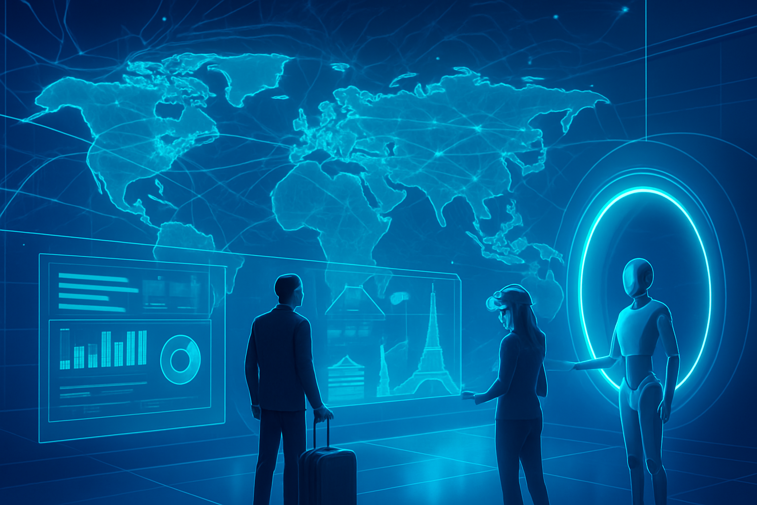
The Technological Vanguard: A Deep Dive into Travel's Digital Revolution
The technological landscape transforming tourism is rich and multifaceted, moving far beyond simple online booking platforms to encompass sophisticated systems that learn, adapt, and create entirely new modes of engagement. At the forefront is Artificial Intelligence (AI), which is making tourism smarter, more personalized, and highly efficient. AI-powered algorithms are optimizing transportation routes for sustainability, predicting busy travel periods for better resource management, and assisting businesses in reducing costs while building stronger customer relationships. Applications range from personalized recommendations and automated customer support chatbots to voice and facial recognition for expedited check-ins, and advanced data analytics that offer profound insights into customer behavior and market trends. This represents a significant leap from previous rule-based systems, offering dynamic, context-aware interactions and predictions.
Virtual Reality (VR) and Augmented Reality (AR) are revolutionizing how travelers engage with destinations, even before they physically arrive. AR overlays digital information onto the real world via devices like smartphones or smart glasses, enriching experiences with interactive visual, auditory, and sensory content. VR, conversely, immerses users entirely in computer-generated environments, allowing them to explore destinations virtually without physical travel. This immersive technology differs vastly from static images or videos, offering a true sense of presence and enabling virtual tours of hotels, historical sites, and attractions. The immersive technologies market is projected to reach US$100 billion by 2026, indicating its growing importance.
Blockchain technology offers significant potential for enhancing security, transparency, and efficiency. It enables secure and traceable payments, simplifies booking processes by connecting travelers directly with service providers, and creates secure digital identities to streamline check-ins. Blockchain can also transform loyalty programs and improve baggage management via sensor tracking. Complementing these are other smart technologies like the Internet of Things (IoT), enabling personalized in-room experiences, biometric recognition for expedited security, and sophisticated mobile applications for navigation and real-time assistance.
FITUR 2026 is poised to be a pivotal showcase for these advancements. The Travel Technology area will see an exceptional 50% expansion, hosting over 150 companies from more than 20 countries. A major development is its relocation to the newly created "Knowledge Hub" in Hall 12, establishing it as the fair's "nerve center" for innovation. This hub will foster dialogue and collaboration on emerging technologies like AI, automation, data analytics, and immersive experiences. FITURTechy 2026, celebrating its 20th edition under the slogan "From Robot to Ally," will delve into the responsible integration of technology, emphasizing an evolution from pure efficiency to innovation that serves people and the planet. This focus on ethical and purposeful technology marks a maturing of the industry's approach, moving beyond mere adoption to thoughtful implementation.
Competitive Landscape: Who Benefits from the Tech Tsunami?
The burgeoning dominance of technology in tourism creates a dynamic competitive landscape, poised to benefit a diverse array of players while posing significant challenges to those slow to adapt. Travel technology startups are uniquely positioned to thrive, offering nimble, specialized solutions in areas like AI-driven personalization, sustainable travel tech, and immersive experiences. Their agility allows them to quickly innovate and fill niche market demands that larger, more established entities might overlook.
Major players like Amadeus (AMS:MCE), Travelgate, and Juniper Travel Technology, all confirmed participants in FITUR 2026's expanded zone, stand to consolidate their market leadership. These established technology providers, already deeply embedded in the travel ecosystem, can leverage their existing infrastructure and client base to integrate and scale new AI and data-driven solutions. Their ability to offer comprehensive platforms covering everything from distribution to customer relationship management will be a significant advantage.
Online Travel Agencies (OTAs) and hospitality giants are also set to benefit immensely from these developments. Companies like Booking Holdings (NASDAQ: BKNG) and Expedia Group (NASDAQ: EXPE) can further refine their recommendation engines, personalize offers, and streamline user experiences through advanced AI. Hotel chains can implement smart room technologies, AI-powered concierge services, and biometric check-ins to enhance guest satisfaction and operational efficiency. The competitive implication is clear: companies that invest heavily in R&D and strategic partnerships within the tech sector will gain substantial market share, potentially disrupting those relying on traditional models. Those failing to embrace digital transformation risk becoming obsolete, as travelers increasingly expect seamless, intelligent, and personalized interactions.
Broader Implications: Reshaping the Global Travel Narrative
The technological revolution in tourism extends far beyond operational efficiencies, deeply embedding itself within broader AI trends and societal shifts. This movement aligns perfectly with the overarching drive towards "smart cities" and "smart destinations," where data-driven insights optimize everything from traffic flow to resource management. The focus on "smart tourism" initiatives, as highlighted by FITUR Know-How & Export 2026's emphasis on the Smart Destination Platform (PID), signifies a strategic move towards holistic, digitally-managed travel ecosystems that enhance visitor experience while promoting sustainability.
The impact on sustainability is particularly profound. AI-powered algorithms can optimize transportation routes to reduce carbon footprints, predict visitor flows to prevent over-tourism, and manage resources more efficiently. FITUR Next 2026's challenge on efficient and sustainable water management further underscores how technology is being leveraged to address critical environmental concerns, aligning with the United Nations Sustainable Development Goals.
However, this rapid technological advancement also brings potential concerns. Issues such as data privacy and cybersecurity become paramount as more personal information is collected and processed. The "From Robot to Ally" slogan of FITURTechy 2026 hints at the crucial need for responsible AI integration, ensuring that technology serves humanity rather than dehumanizing interactions or leading to job displacement without adequate reskilling initiatives. Compared to previous milestones like the advent of online booking, which primarily digitized existing processes, the current wave of AI, VR, and blockchain represents a more fundamental transformation, creating entirely new possibilities for interaction, personalization, and operational models.
The Horizon of Travel: Anticipating Future Developments
Looking ahead, the trajectory of technology in tourism promises even more groundbreaking innovations. In the near term, we can expect to see an accelerated deployment of hyper-personalized AI agents that act as virtual travel concierges, capable of understanding complex preferences, dynamically adjusting itineraries in real-time, and offering predictive assistance. The proliferation of metaverse travel experiences will likely grow, allowing individuals to explore destinations virtually before booking, or even to "travel" to inaccessible or historical locations from the comfort of their homes. Further integration of biometric identification for seamless, touchless journeys from airport check-in to hotel room access is also on the horizon.
Longer term, experts predict the rise of fully autonomous travel systems, where AI optimizes every aspect of a trip, from transportation to accommodation, with minimal human intervention. The widespread adoption of blockchain-based digital identities could fundamentally alter how we manage travel documents and loyalty programs, creating a more secure and interoperable global travel network. Challenges that need to be addressed include developing robust ethical frameworks for AI, ensuring equitable access to these technologies, and safeguarding against potential misuse of personal data. Experts predict a future where travel becomes an increasingly invisible, yet deeply personalized, experience, driven by intelligent systems that anticipate our needs before we even articulate them.
A New Epoch for Exploration: Wrapping Up the Digital Journey
In summary, the expansion of FITUR 2026's Travel Technology Zone is not merely an exhibition update; it is a powerful declaration that technology has become the undisputed "new king" of tourism. The key takeaways are clear: AI, VR/AR, blockchain, and IoT are no longer emerging concepts but foundational pillars transforming how we discover, book, experience, and manage travel. This development signifies a profound shift from a service-oriented industry to a technology-driven one, where innovation dictates the pace of progress.
This moment marks a significant chapter in the history of tourism, moving beyond the digital revolution of the early 2000s into an era of intelligent and immersive travel. The emphasis on responsible integration, as seen in FITURTechy's "From Robot to Ally" theme, highlights a maturing industry that seeks to leverage technology not just for profit, but for people and the planet.
In the coming weeks and months, watch for announcements from major travel brands regarding their AI and immersive technology investments, further partnerships between tech firms and tourism entities, and the continued evolution of regulatory frameworks addressing data privacy and ethical AI in travel. The journey ahead promises to be as exciting and transformative as the destinations themselves.
This content is intended for informational purposes only and represents analysis of current AI developments.
TokenRing AI delivers enterprise-grade solutions for multi-agent AI workflow orchestration, AI-powered development tools, and seamless remote collaboration platforms.
For more information, visit https://www.tokenring.ai/.