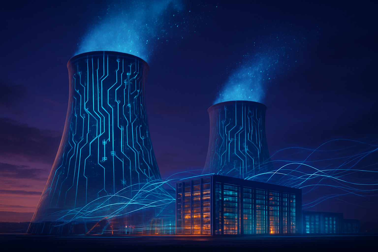
In a move that signals a paradigm shift in how the tech industry fuels its digital expansion, Microsoft (NASDAQ: MSFT) has secured a landmark agreement to restart a shuttered reactor at the infamous Three Mile Island nuclear facility. As of January 2026, the deal between the tech giant and Constellation Energy (NASDAQ: CEG) represents the most aggressive step yet by a "hyperscaler" to solve the "energy trilemma": the need for massive, reliable, and carbon-free power to sustain the ongoing generative AI revolution.
The project, officially rebranded as the Crane Clean Energy Center, aims to bring 835 megawatts (MW) of carbon-free electricity back to the grid—enough to power roughly 800,000 homes. However, this power won’t be heating houses; it is destined for the energy-hungry data center clusters that underpin Microsoft’s Azure cloud and its multi-billion-dollar investments in OpenAI. This resurrection of a mothballed nuclear plant is the clearest sign yet that the 2026 data center boom has outpaced the capabilities of wind and solar, forcing the world’s most powerful companies to embrace the atom to keep their AI models running 24/7.
The Resurrection of Unit 1: Technical Ambition and the 2027 Timeline
The Crane Clean Energy Center focuses exclusively on Three Mile Island Unit 1, a reactor that operated safely for decades before being closed for economic reasons in 2019. This is distinct from Unit 2, which has remained dormant since its partial meltdown in 1979. As of late January 2026, Constellation Energy reports that the restart project is running ahead of its original 2028 schedule, with a new target for grid synchronization in 2027. This acceleration is driven by a massive infusion of capital and a "war room" approach to regulatory hurdles, supported by a $1 billion federal loan granted in late 2025 to fast-track domestic AI energy security.
Technically, the restart involves a comprehensive overhaul of the facility’s primary and secondary systems. Engineers are currently focused on the restoration of cooling systems, control room modernization, and the replacement of large-scale components like the main power transformers. Unlike traditional grid additions, this project is a "brownfield" redevelopment, leveraging existing infrastructure that already has a footprint for high-voltage transmission. This gives Microsoft a significant advantage over competitors trying to build new plants from scratch, as the permitting process for an existing site—while rigorous—is substantially faster than for a "greenfield" nuclear project.
The energy industry has reacted with a mix of awe and pragmatism. While some environmental groups remain cautious about the long-term waste implications, the consensus among energy researchers is that Microsoft is providing a blueprint for "firm" carbon-free power. Unlike intermittent sources such as solar or wind, which require massive battery storage to support data centers through the night, nuclear provides a steady "baseload" of electricity. This 100% "capacity factor" is critical for training the next generation of Large Language Models (LLMs) that require months of uninterrupted, high-intensity compute cycles.
The Nuclear Arms Race: How Big Tech is Dividing the Grid
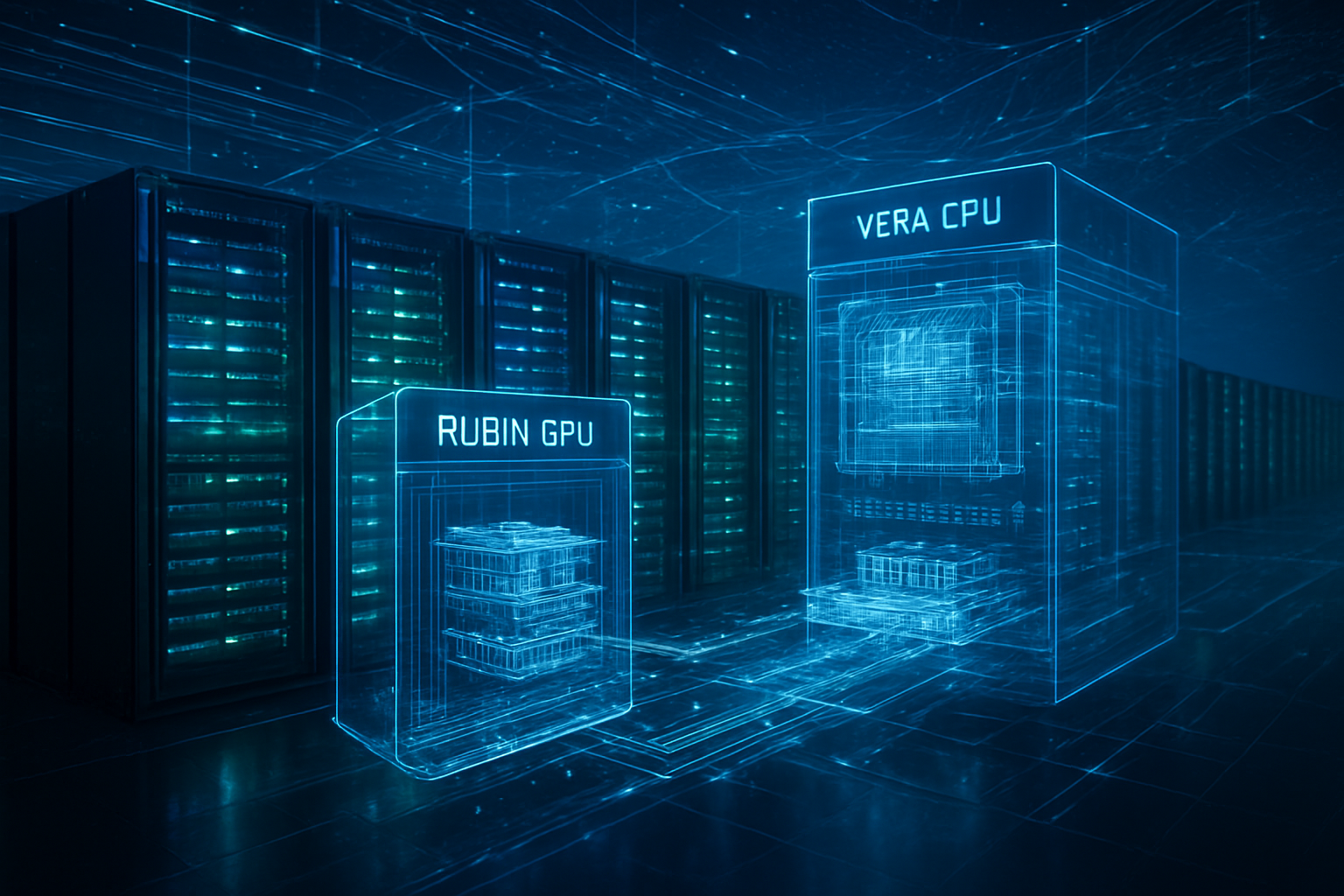
Microsoft’s deal has ignited a "nuclear arms race" among Big Tech firms, fundamentally altering the competitive landscape of the cloud industry. Amazon (NASDAQ: AMZN) recently countered by expanding its agreement with Talen Energy to secure nearly 2 gigawatts (GW) of power from the Susquehanna Steam Electric Station. Meanwhile, Alphabet (NASDAQ: GOOGL) has taken a different path, focusing on the future of Small Modular Reactors (SMRs) through a partnership with Kairos Power to deploy a fleet of 500 MW by the early 2030s.
The strategic advantage of these deals is twofold: price stability and capacity reservation. By signing a 20-year fixed-price Power Purchase Agreement (PPA), Microsoft is insulating itself from the volatility of the broader energy market. In the 2026 landscape, where electricity prices have spiked due to the massive demand from AI and the electrification of transport, owning a dedicated "clean electron" source is a major competitive moat. Smaller AI startups and mid-tier cloud providers are finding themselves increasingly priced out of the market, as tech giants scoop up the remaining available baseload capacity.
This trend is also shifting the geographical focus of the tech industry. We are seeing a "rust belt to tech belt" transformation, as regions with existing nuclear infrastructure—like Pennsylvania, Illinois, and Iowa—become the new hotspots for data center construction. Companies like Meta Platforms (NASDAQ: META) have also entered the fray, recently announcing plans to procure up to 6.6 GW of nuclear energy by 2035 through partnerships with Vistra (NYSE: VST) and advanced reactor firms like Oklo (NYSE: OKLO). The result is a market where "clean energy" is no longer just a corporate social responsibility (CSR) goal, but a core requirement for operational survival.
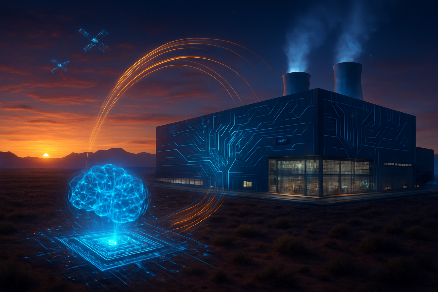
Beyond the Cooling Towers: AI’s Impact on Global Energy Policy
The intersection of AI and nuclear energy is more than a corporate trend; it is a pivotal moment in the global energy transition. For years, the tech industry led the charge into renewables, but the 2026 AI infrastructure surge—with capital expenditures expected to exceed $600 billion this year alone—has exposed the limitations of current grid technologies. AI’s demand for electricity is growing at a rate that traditional utilities struggle to meet, leading to a new era of "behind-the-meter" solutions where tech companies effectively become their own utility providers.
This shift has profound implications for climate goals. While the reliance on nuclear power helps Microsoft and its peers stay on track for "carbon negative" targets, it also raises questions about grid equity. If tech giants monopolize the cleanest and most reliable energy sources, local communities may be left with the more volatile or carbon-heavy portions of the grid. However, proponents argue that Big Tech’s massive investments are essentially subsidizing the "Nuclear Renaissance," paying for the innovation and safety upgrades that will eventually benefit all energy consumers.
The move also underscores a national security narrative. In early 2026, the U.S. government has increasingly viewed AI dominance as inextricably linked to energy dominance. By facilitating the restart of Three Mile Island, federal regulators are acknowledging that the "AI race" against global competitors cannot be won on an aging and overstressed power grid. This has led to the Nuclear Regulatory Commission (NRC) streamlining licensing for restarts and SMRs, a policy shift that would have been unthinkable just five years ago.
The Horizon: From Restarts to Fusion and SMRs
Looking ahead, the Three Mile Island restart is widely viewed as a bridge to more advanced energy technologies. While gigawatt-scale reactors provide the bulk of the power needed today, the near-term future belongs to Small Modular Reactors (SMRs). These factory-built units promise to be safer and more flexible, allowing tech companies to place power sources directly adjacent to data center campuses. Experts predict that the first commercial SMRs will begin coming online by 2029, with Microsoft and Google already scouting locations for these "micro-grids."
Beyond SMRs, the industry is keeping a close eye on nuclear fusion. Microsoft’s existing deal with Helion Energy, which aims to provide fusion power as early as 2028, remains a high-stakes bet. While technical challenges persist, the sheer amount of capital being poured into the sector by AI-wealthy firms is accelerating R&D at an unprecedented pace. The challenge remains the supply chain: the industry must now scale up the production of specialized fuels and high-tech components to meet the demand for dozens of new reactors simultaneously.
Predictions for the next 24 months suggest a wave of "restart" announcements for other decommissioned plants across the U.S. and Europe. Companies like NextEra Energy are reportedly evaluating the Duane Arnold Energy Center in Iowa for a similar revival. As AI models grow in complexity—with "GPT-6" class models rumored to require power levels equivalent to small cities—the race to secure every available megawatt of carbon-free energy will only intensify.
A New Era for Intelligence and Energy
The resurrection of Three Mile Island Unit 1 is a watershed moment in the history of technology. It marks the end of the era where software could be scaled independently of physical infrastructure. In 2026, the "cloud" is more grounded in reality than ever, tethered to the massive turbines and cooling towers of the nuclear age. Microsoft’s decision to link its AI future to a once-shuttered reactor is a bold acknowledgement that the path to artificial general intelligence (AGI) is paved with clean, reliable energy.
The key takeaway for the industry is that the energy bottleneck is the new "silicon shortage." Just as GPU availability defined the winners of 2023 and 2024, energy availability is defining the winners of 2026. As the Crane Clean Energy Center moves toward its 2027 restart, the tech world will be watching closely. Its success—or failure—will determine whether nuclear energy becomes the permanent foundation of the AI era or a costly detour in the search for a sustainable digital future.
In the coming months, expect more "hyperscaler" deals with specialized energy providers and a continued push for regulatory reform. The 2026 data center boom has made one thing certain: the future of AI will not just be written in code, but forged in the heart of the atom.
This content is intended for informational purposes only and represents analysis of current AI developments.
TokenRing AI delivers enterprise-grade solutions for multi-agent AI workflow orchestration, AI-powered development tools, and seamless remote collaboration platforms.
For more information, visit https://www.tokenring.ai/.