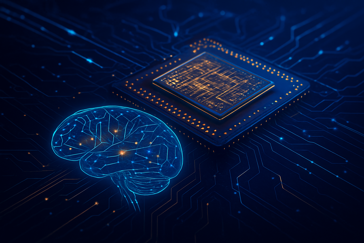
Tag: AI

  • USPTO’s AI Renaissance: Director Squires Ushers in a New Era for Intellectual Property

    USPTO’s AI Renaissance: Director Squires Ushers in a New Era for Intellectual Property

    Washington D.C., October 31, 2025 – The U.S. Patent and Trademark Office (USPTO) is undergoing a significant transformation under the leadership of its new Director, John Squires, who assumed office in September 2025. Squires has unequivocally placed Artificial Intelligence (AI) at the zenith of the agency's priorities, signaling a profound recalibration of how AI-related inventions are treated within the intellectual property (IP) landscape. This strategic pivot, unfolding even amidst broader governmental challenges, is poised to reshape the future of AI innovation in the United States, offering clearer pathways for innovators while addressing the complex challenges posed by rapidly advancing technology.

    Director Squires' immediate emphasis on AI marks a decisive shift towards fostering, rather than hindering, AI innovation through patent protection. This move is largely driven by a recognition of AI's critical role in global competitiveness, the burgeoning volume of AI-related patent applications, and an urgent need to modernize the patent system. The USPTO's renewed focus aims to provide greater certainty and encouragement for inventors and companies investing heavily in AI research and development, ensuring that America remains at the forefront of this transformative technological wave.

    A Paradigm Shift in AI Patentability and Examination

    The core of Director Squires' AI initiative lies in a significant reinterpretation of subject matter eligibility for AI inventions, particularly under 35 U.S.C. § 101, which has historically been a major hurdle for AI patent applicants. Moving away from previous restrictive interpretations that often categorized AI innovations as unpatentable abstract ideas, the USPTO is now adopting a more patentee-friendly approach. This is exemplified by the unusual step of convening an Appeals Review Panel (ARP) to overturn prior Patent Trial and Appeal Board (PTAB) decisions that had rejected AI patent applications on abstract idea grounds.

    This shift redirects the focus of patent examination towards traditional patentability requirements such as novelty (35 U.S.C. § 102), non-obviousness (35 U.S.C. § 103), and adequate written description and enablement (35 U.S.C. § 112). The goal is to prevent the overly restrictive application of Section 101 from stifling legitimate AI innovations. Consequently, initial reactions from the AI research community and industry experts have been largely positive, with many anticipating an increase in AI/Machine Learning (ML)-related patent application filings and grants, as the relaxed standards provide a more predictable and accessible path to patentability.

    To further streamline the process and improve efficiency, the USPTO has launched an Artificial Intelligence Pilot Program for pre-examination searches. This innovative program allows applicants to receive AI-generated search reports before a human examiner reviews the application, aiming to provide earlier insights and potentially reduce examination times. While embracing AI's role in the patent process, the USPTO firmly maintains the human inventorship requirement, stipulating that any AI-assisted invention still necessitates a "significant contribution by a human inventor" to be patent eligible, thus upholding established IP principles. These efforts align with the USPTO's broader 2025 Artificial Intelligence Strategy, published in January 2025, which outlines a comprehensive vision for advancing inclusive AI innovation, building best-in-class AI capabilities, promoting responsible AI use, developing workforce expertise, and fostering collaboration on shared AI priorities.

    Unleashing Innovation: Implications for AI Companies and Tech Giants

    The USPTO's invigorated stance on AI patentability under Director Squires is set to profoundly reshape the competitive dynamics within the artificial intelligence sector. By easing the stringent "abstract idea" rejections under 35 U.S.C. § 101, especially highlighted by the Ex parte Desjardins decision in September 2025, the office is effectively lowering barriers for securing intellectual property protection for novel AI algorithms, models, and applications. This policy shift is a boon for a wide spectrum of players, from agile AI startups to established tech behemoths.

    AI companies and burgeoning startups, often built upon groundbreaking but previously hard-to-patent AI methodologies, stand to gain significantly. Stronger IP portfolios will not only enhance their valuation and attractiveness to investors but also provide a crucial competitive edge in a crowded market. For major tech giants such as Alphabet (NASDAQ: GOOGL) (parent company of Google), Microsoft (NASDAQ: MSFT), and IBM (NYSE: IBM), which possess vast AI research and development capabilities and extensive existing patent portfolios, the new guidelines offer an accelerated path to fortify their dominance. The Ex parte Desjardins case itself, involving a Google AI-related patent application, underscores how this shift directly benefits these large players, enabling them to further entrench their positions in foundational AI technologies and complex AI systems.

    The competitive landscape is expected to intensify, potentially leading to an increase in AI patent filings and, consequently, more robust "IP wars." Companies will likely reorient their R&D strategies to emphasize "technical improvements" and practical applications, ensuring their innovations align with the new patentability criteria. This could lead to an acceleration of innovation cycles, as enhanced patent protection incentivizes greater investment in R&D and the rapid introduction of new AI-driven products and services. Furthermore, stronger AI patents can foster dynamic licensing markets, allowing innovators to commercialize their IP through strategic partnerships and licensing agreements, thereby shaping the broader AI technology ecosystem and potentially disrupting existing product offerings as proprietary AI features become key differentiators. For all entities, a sophisticated IP strategy—encompassing aggressive filing, meticulous claim drafting, and diligent inventorship documentation—becomes paramount for securing and maintaining market positioning and strategic advantages.

    A Broader Horizon: AI in the Global IP Landscape

    The USPTO's proactive stance on AI patentability under Director John Squires is not merely an internal adjustment but a significant move within the broader global AI landscape. Director Squires has explicitly warned against "categorically excluding AI innovations from patent protection," recognizing that such a policy would jeopardize America's leadership in this critical emerging technology. This perspective aligns with a growing international consensus that intellectual property frameworks must adapt to foster, rather than impede, AI development. The landmark Ex parte Desjardins decision on September 30, 2025, which deemed a machine learning-based invention patent-eligible by emphasizing its "technical improvements," serves as a clear beacon for this new direction.

    This shift prioritizes the traditional pillars of patentability—novelty, non-obviousness, and adequate disclosure—over the often-contentious "abstract idea" rejections under 35 U.S.C. § 101 that have historically plagued software and AI inventions. By focusing on whether an AI innovation provides a "technical solution to a technical problem" and demonstrates "technical improvements," the USPTO is establishing clearer, more predictable guidelines for inventors. This approach mirrors evolving global discussions, particularly within organizations like the World Intellectual Property Organization (WIPO), which are actively grappling with how to best integrate AI into existing IP paradigms while maintaining the foundational principle of human inventorship, as reinforced by the USPTO's February 2024 guidance and the Federal Circuit's 2022 Thaler v. Vidal ruling.

    However, this more permissive environment also introduces potential concerns. One significant apprehension is the rise of "bionic patent trolls"—non-practicing entities (NPEs) that might leverage AI to generate numerous thinly patentable inventions, automate infringement detection, and mass-produce demand letters. With over 50% of AI-related patent lawsuits already initiated by NPEs, there's a risk of stifling genuine innovation, particularly for startups, by diverting resources into defensive litigation. Furthermore, ethical considerations surrounding AI, such as bias, transparency, and accountability, remain paramount. The "black box" problem, where the decision-making processes of complex AI systems are opaque, presents challenges for patent examination and enforcement. The potential for oversaturation of the patent system and the concentration of ownership among a few powerful entities using advanced generative AI to build "patent walls" also warrant careful monitoring. This current policy shift represents a direct and significant departure from the restrictive interpretations that followed the 2014 Alice Corp. v. CLS Bank Int'l Supreme Court decision, positioning the USPTO at the forefront of modernizing IP law to meet the unique challenges and opportunities presented by advanced AI.

    The Road Ahead: Navigating AI's Evolving Patent Frontier

    The USPTO's invigorated focus on AI patent policy under Director John Squires sets the stage for a dynamic period of evolution in intellectual property. In the near term, the office is committed to refining its guidance for examiners and the public. This includes the February 2024 clarification that only natural persons can be named as inventors, emphasizing a "significant human contribution" even when AI tools are utilized. Further enhancing subject matter eligibility, an August 2025 memo to examiners and the July 2024 guidance are expected to bolster patent eligibility for AI/Machine Learning (ML) technologies by clarifying that AI inventions incapable of practical human mental performance are not abstract ideas. These adjustments are already triggering a surge in AI/ML patent filings and grants, promising faster and more cost-effective protection. Internally, the USPTO is heavily investing in AI-driven tools for examination and workforce expertise, while also issuing ethical guidance for legal practitioners using AI, a first among federal agencies.

    Looking further ahead, the long-term trajectory involves deeper integration of AI into the patent system and potential legislative shifts. The fundamental question of AI inventorship will continue to evolve; while currently restricted to humans, advancements in generative AI might necessitate policy adjustments or even legislative changes as AI's creative capabilities grow. Addressing AI-generated prior art is another critical area, as the proliferation of AI-created content could impact patent validity. The USPTO will likely issue more refined examination guidelines, particularly demanding more stringent standards for enablement and written description for AI applications, requiring detailed descriptions of inputs, outputs, correlations, and test results. International harmonization of AI IP policies, through collaborations with global partners, will also be crucial as AI becomes a universal technological foundation.

    The potential applications and use cases for AI-related patents are vast and ever-expanding. Beyond predictive and generative AI in areas like financial forecasting, medical diagnostics, and content creation, patents are emerging in highly specialized domains. These include AI-driven heart monitoring systems, autonomous vehicle navigation algorithms, cybersecurity threat detection, cloud computing optimization, realistic gaming AI, and smart manufacturing. Notably, AI is also being patented for its role within the patent process itself—assisting with prior art searches, predicting application outcomes, drafting patent claims, and aiding in litigation analysis.

    Despite the promising outlook, significant challenges persist. The definition of "significant human contribution" for AI-generated inventions remains a complex legal and philosophical hurdle. Distinguishing patent-eligible practical applications from unpatentable "abstract ideas" for AI algorithms continues to be a nuanced task. The "black box" problem, referring to the opacity of complex AI systems, makes it difficult to meet the detailed disclosure requirements for patent applications. The rapid evolution of AI technology itself poses a challenge, as innovations can quickly become outdated, and the definition of a "person having ordinary skill in the art" (PHOSITA) in the AI context becomes increasingly fluid. Experts predict a continued focus on human contribution, increased scrutiny on enablement and written description, and the growing role of AI tools for patent professionals, all while the patent landscape becomes more diverse with AI innovation diffusing into smaller businesses and new patent categories emerging.

    The Dawn of a Patent-Friendly AI Era: A Comprehensive Wrap-Up

    Director John Squires' emphatic prioritization of Artificial Intelligence at the U.S. Patent and Trademark Office marks a pivotal moment in the history of intellectual property. His actions, from convening an Appeals Review Panel to overturn restrictive AI patent rejections to launching AI-powered pilot programs, signal a clear intent to foster, rather than inhibit, AI innovation through robust patent protection. This strategic pivot, unfolding rapidly since his appointment in September 2025, is a direct response to the escalating importance of AI in global competitiveness, the explosion of AI-related patent filings, and the imperative to modernize the patent system for the 21st century.

    The significance of this development cannot be overstated. By shifting the focus from overly broad "abstract idea" rejections to traditional patentability requirements like novelty and non-obviousness, the USPTO is providing much-needed clarity and predictability for AI innovators. This change stands in stark contrast to the more restrictive interpretations of Section 101 that characterized the post-Alice Corp. era, positioning the U.S. as a more attractive jurisdiction for securing AI-related intellectual property. While promising to accelerate innovation, this new landscape also necessitates careful navigation of potential pitfalls, such as the rise of "bionic patent trolls" and the ethical challenges surrounding AI bias and transparency.

    In the coming weeks and months, the tech world will be watching closely for further refinements in USPTO guidance, particularly concerning the nuanced definition of "significant human contribution" in AI-assisted inventions and the treatment of AI-generated prior art. Companies, from established tech giants like Alphabet (NASDAQ: GOOGL) and Microsoft (NASDAQ: MSFT) to nimble AI startups, must adopt proactive and sophisticated IP strategies, emphasizing detailed disclosures and leveraging the USPTO's evolving resources. This new era under Director Squires is not just about more patents; it's about shaping an intellectual property framework that can truly keep pace with, and propel forward, the unprecedented advancements in artificial intelligence, ensuring that innovation continues to thrive responsibly.


    This content is intended for informational purposes only and represents analysis of current AI developments.

    TokenRing AI delivers enterprise-grade solutions for multi-agent AI workflow orchestration, AI-powered development tools, and seamless remote collaboration platforms.
    For more information, visit https://www.tokenring.ai/.

  • Wikipedia Founder Jimmy Wales Warns of AI’s ‘Factual Blind Spot,’ Challenges to Verifiable Truth

    Wikipedia Founder Jimmy Wales Warns of AI’s ‘Factual Blind Spot,’ Challenges to Verifiable Truth

    New York, NY – October 31, 2025 – Wikipedia co-founder Jimmy Wales has issued a stark warning regarding the inherent "factual blind spot" of artificial intelligence, particularly large language models (LLMs), asserting that their current capabilities pose a significant threat to verifiable truth and could accelerate the proliferation of misinformation. His recent statements, echoing long-held concerns, underscore a fundamental tension between the fluency of AI-generated content and its often-dubious accuracy, drawing a clear line between the AI's approach and Wikipedia's rigorous, human-centric model of knowledge creation.

    Wales' criticisms highlight a growing apprehension within the information integrity community: while LLMs can produce seemingly authoritative and coherent text, they frequently fabricate details, cite non-existent sources, and present plausible but factually incorrect information. This propensity, which Wales colorfully terms "AI slop," represents a profound challenge to the digital information ecosystem, demanding renewed scrutiny of how AI is integrated into platforms designed for public consumption of knowledge.

    The Technical Chasm: Fluency vs. Factuality in Large Language Models

    At the core of Wales' concern is the architectural design and operational mechanics of large language models. Unlike traditional databases or curated encyclopedias, LLMs are trained to predict the next most probable word in a sequence based on vast datasets, rather than to retrieve and verify discrete facts. This predictive nature, while enabling impressive linguistic fluidity, does not inherently guarantee factual accuracy. Wales points to instances where LLMs consistently provide "plausible but wrong" answers, even about relatively obscure but verifiable individuals, demonstrating their inability to "dig deeper" into precise factual information.

    A notable example of this technical shortcoming recently surfaced within the German Wikipedia community. Editors uncovered research papers containing fabricated references, with authors later admitting to using tools like ChatGPT to generate citations. This incident perfectly illustrates the "factual blind spot": the AI prioritizes generating a syntactically correct and contextually appropriate citation over ensuring its actual existence or accuracy. This approach fundamentally differs from Wikipedia's methodology, which mandates that all information be verifiable against reliable, published sources, with human editors meticulously checking and cross-referencing every claim. Furthermore, in August 2025, Wikipedia's own community of editors decisively rejected Wales' proposal to integrate AI tools like ChatGPT into their article review process after an experiment revealed the AI's failure to meet Wikipedia's core policies on neutrality, verifiability, and reliable sourcing. This rejection underscores the deep skepticism within expert communities about the current technical readiness of LLMs for high-stakes information environments.

    Competitive Implications and Industry Scrutiny for AI Giants

    Jimmy Wales' pronouncements place significant pressure on the major AI developers and tech giants investing heavily in large language models. Companies like Google (NASDAQ: GOOGL), Microsoft (NASDAQ: MSFT), and OpenAI, which are at the forefront of LLM development and deployment, now face intensified scrutiny regarding the factual reliability of their products. The "factual blind spot" directly impacts the credibility and trustworthiness of AI-powered search, content generation, and knowledge retrieval systems being integrated into mainstream applications.

    Elon Musk's ambitious "Grokipedia" project, an AI-powered encyclopedia, has been singled out by Wales as particularly susceptible to these issues. At the CNBC Technology Executive Council Summit in New York in October 2025, Wales predicted that such a venture, heavily reliant on LLMs, would suffer from "massive errors." This perspective highlights a crucial competitive battleground: the race to build not just powerful, but trustworthy AI. Companies that can effectively mitigate the factual inaccuracies and "hallucinations" of LLMs will gain a significant strategic advantage, potentially disrupting existing products and services that prioritize speed and volume over accuracy. Conversely, those that fail to address these concerns risk eroding public trust and facing regulatory backlash, impacting their market positioning and long-term viability in the rapidly evolving AI landscape.

    Broader Implications: The Integrity of Information in the Digital Age

    The "factual blind spot" of large language models extends far beyond technical discussions, posing profound challenges to the broader landscape of information integrity and the fight against misinformation. Wales argues that while generative AI is a concern, social media algorithms that steer users towards "conspiracy videos" and extremist viewpoints might have an even greater impact on misinformation. This perspective broadens the discussion, suggesting that the problem isn't solely about AI fabricating facts, but also about how information, true or false, is amplified and consumed.

    The rise of "AI slop"—low-quality, machine-generated articles—threatens to dilute the overall quality of online information, making it increasingly difficult for individuals to discern reliable sources from fabricated content. This situation underscores the critical importance of media literacy, particularly for older internet users who may be less accustomed to the nuances of AI-generated content. Wikipedia, with its transparent editorial practices, global volunteer community, and unwavering commitment to neutrality, verifiability, and reliable sourcing, stands as a critical bulwark against this tide. Its model, honed over two decades, offers a tangible alternative to the unchecked proliferation of AI-generated content, demonstrating that human oversight and community-driven verification remain indispensable in maintaining the integrity of shared knowledge.

    The Road Ahead: Towards Verifiable and Responsible AI

    Addressing the "factual blind spot" of large language models represents one of the most significant challenges for AI development in the coming years. Experts predict a dual approach will be necessary: technical advancements coupled with robust ethical frameworks and human oversight. Near-term developments are likely to focus on improving fact-checking mechanisms within LLMs, potentially through integration with knowledge graphs or enhanced retrieval-augmented generation (RAG) techniques that ground AI responses in verified data. Research into "explainable AI" (XAI) will also be crucial, allowing users and developers to understand why an AI produced a particular answer, thus making factual errors easier to identify and rectify.

    Long-term, the industry may see the emergence of hybrid AI systems that seamlessly blend the generative power of LLMs with the rigorous verification capabilities of human experts or specialized, fact-checking AI modules. Challenges include developing robust methods to prevent "hallucinations" and biases embedded in training data, as well as creating scalable solutions for continuous factual verification. What experts predict is a future where AI acts more as a sophisticated assistant to human knowledge workers, rather than an autonomous creator of truth. This shift would prioritize AI's utility in summarizing, synthesizing, and drafting, while reserving final judgment and factual validation for human intelligence, aligning more closely with the principles championed by Jimmy Wales.

    A Critical Juncture for AI and Information Integrity

    Jimmy Wales' recent and ongoing warnings about AI's "factual blind spot" mark a critical juncture in the evolution of artificial intelligence and its societal impact. His concerns serve as a potent reminder that technological prowess, while impressive, must be tempered with an unwavering commitment to truth and accuracy. The proliferation of large language models, while offering unprecedented capabilities for content generation, simultaneously introduces unprecedented challenges to the integrity of information.

    The key takeaway is clear: the pursuit of ever more sophisticated AI must go hand-in-hand with the development of equally sophisticated mechanisms for verification and accountability. The contrast between AI's "plausible but wrong" output and Wikipedia's meticulously sourced and community-verified knowledge highlights a fundamental divergence in philosophy. As AI continues its rapid advancement, the coming weeks and months will be crucial in observing how AI companies respond to these criticisms, whether they can successfully engineer more factually robust models, and how society adapts to a world where discerning truth from "AI slop" becomes an increasingly vital skill. The future of verifiable information hinges on these developments.


    This content is intended for informational purposes only and represents analysis of current AI developments.

    TokenRing AI delivers enterprise-grade solutions for multi-agent AI workflow orchestration, AI-powered development tools, and seamless remote collaboration platforms.
    For more information, visit https://www.tokenring.ai/.

  • LeapXpert’s AI Unleashes a New Era of Order and Accountability in Business Messaging

    LeapXpert’s AI Unleashes a New Era of Order and Accountability in Business Messaging

    San Francisco, CA – October 31, 2025 – In a significant stride towards harmonizing the often-conflicting demands of innovation and compliance, LeapXpert, a leading provider of enterprise-grade messaging solutions, has introduced a groundbreaking AI-powered suite designed to instill unprecedented levels of order, oversight, and accountability in business communications. Launched in March 2024 with its Maxen™ Generative AI application, and further bolstered by its Messaging Security Package in November 2024, LeapXpert's latest offerings are reshaping how global enterprises manage client interactions across the fragmented landscape of modern messaging platforms.

    The introduction of these advanced AI capabilities marks a pivotal moment for industries grappling with regulatory pressures while striving for enhanced client engagement and operational efficiency. By leveraging artificial intelligence, LeapXpert enables organizations to embrace the agility and ubiquity of consumer messaging apps like WhatsApp, iMessage, and WeChat for business purposes, all while maintaining rigorous adherence to compliance standards. This strategic move addresses the long-standing challenge of "dark data" – unmonitored and unarchived communications – transforming a potential liability into a structured, auditable asset for enterprises worldwide.

    Technical Prowess: AI-Driven Precision for Enterprise Communications

    At the heart of LeapXpert's new solution lies Maxen™, a patented Generative AI (GenAI) application that generates "Communication Intelligence" by integrating data from diverse communication sources. Maxen™ provides relationship managers with live insights and recommendations based on recent communications, suggesting impactful message topics and content. This not only standardizes communication quality but also significantly boosts productivity by assisting in the creation of meeting agendas, follow-ups, and work plans. Crucially, Maxen™ incorporates robust fact and compliance checking for every message, ensuring integrity and adherence to regulatory standards in real-time.

    Complementing Maxen™ is the broader LeapXpert Communications Platform, built on the Federated Messaging Orchestration Platform (FMOP), which acts as a central hub for managing business communications across various channels. The platform assigns employees a "Single Professional Identity™," consolidating client communications (voice, SMS, WhatsApp, iMessage, WeChat, Telegram, LINE, Signal) under one business number accessible across corporate and personal devices. This centralized approach simplifies interactions and streamlines monitoring. Furthermore, the Messaging Security Package, launched nearly a year ago, introduced an AI-driven Impersonation Detection system that analyzes linguistic and behavioral patterns to flag potential impersonation attempts in real-time. This package also includes antivirus/anti-malware scanning and Content Disarm and Reconstruction (CDR) to proactively neutralize malicious content, offering a multi-layered defense far exceeding traditional, reactive security measures.

    What sets LeapXpert's approach apart from previous methods is its proactive, integrated compliance. Instead of merely archiving communications after the fact, the AI actively participates in the communication process—offering guidance, checking facts, and detecting threats before they can cause harm. Traditional solutions often relied on blanket restrictions or cumbersome, separate applications that hindered user experience and adoption. LeapXpert's solution, however, embeds governance directly into the popular messaging apps employees and clients already use, bridging the gap between user convenience and corporate control. This seamless integration with leading archiving systems (e.g., MirrorWeb, Veritas, Behavox) ensures granular data ingestion and meticulous recordkeeping, providing tamper-proof audit trails vital for regulatory compliance.

    Initial reactions from the AI research community and industry experts have been largely positive, highlighting the solution's innovative use of GenAI for proactive compliance. Analysts commend LeapXpert for tackling a persistent challenge in financial services and other regulated industries where the rapid adoption of consumer messaging has created significant compliance headaches. The ability to maintain a single professional identity while enabling secure, monitored communication across diverse platforms is seen as a significant leap forward.

    Competitive Implications and Market Dynamics

    LeapXpert's new AI solution positions the company as a formidable player in the enterprise communication and compliance technology space. While LeapXpert itself is a private entity, its advancements have significant implications for a range of companies, from established tech giants to nimble startups. Companies in highly regulated sectors, such as financial services, healthcare, and legal, stand to benefit immensely from a solution that de-risks modern communication channels.

    The competitive landscape sees major cloud communication platforms and enterprise software providers, including those offering unified communications as a service (UCaaS), facing pressure to integrate similar robust compliance and AI-driven oversight capabilities. While companies like Microsoft (NASDAQ: MSFT) with Teams, Salesforce (NYSE: CRM) with Slack, or Zoom Video Communications (NASDAQ: ZM) offer extensive communication tools, LeapXpert's specialized focus on federating consumer messaging apps for enterprise compliance offers a distinct advantage in a niche that these larger players have historically struggled to fully address. The potential disruption to existing compliance and archiving services that lack real-time AI capabilities is substantial, as LeapXpert's proactive approach could render reactive solutions less effective.

    LeapXpert's market positioning is strengthened by its ability to offer both innovation and compliance in a single, integrated platform. This strategic advantage allows enterprises to adopt customer-centric communication strategies without compromising security or regulatory adherence. By transforming "dark data" into auditable records, LeapXpert not only mitigates risk but also unlocks new avenues for data-driven insights from client interactions, potentially influencing product development and service delivery strategies for its enterprise clients. The company’s continued focus on integrating cutting-edge AI, as demonstrated by the recent launches, ensures it remains at the forefront of this evolving market.

    Wider Significance in the AI Landscape

    LeapXpert's AI solution is more than just a product update; it represents a significant development within the broader AI landscape, particularly in the domain of responsible AI and AI for governance. It exemplifies a growing trend where AI is not merely used for efficiency or creative generation but is actively deployed to enforce rules, ensure integrity, and maintain accountability in complex human interactions. This fits squarely into the current emphasis on ethical AI, demonstrating how AI can be a tool for good governance, rather than solely a source of potential risk.

    The impact extends to redefining how organizations perceive and manage communication risks. Historically, the adoption of new, informal communication channels has been met with either outright bans or inefficient, manual oversight. LeapXpert's AI flips this paradigm, enabling innovation by embedding compliance. This has profound implications for industries struggling with regulatory mandates like MiFID II, Dodd-Frank, and GDPR, as it offers a practical pathway to leverage modern communication tools without incurring severe penalties.

    Potential concerns, however, always accompany powerful AI solutions. Questions around data privacy, the potential for AI biases in communication analysis, and the continuous need for human oversight to validate AI-driven decisions remain pertinent. While LeapXpert emphasizes robust data controls and tamper-proof storage, the sheer volume of data processed by such systems necessitates ongoing vigilance. This development can be compared to previous AI milestones that automated complex tasks; however, its unique contribution lies in automating compliance and oversight in real-time, moving beyond mere data capture to active, intelligent intervention. It underscores the maturation of AI from a purely analytical tool to an active participant in maintaining organizational integrity.

    Exploring Future Developments

    Looking ahead, the trajectory of solutions like LeapXpert's suggests several exciting near-term and long-term developments. In the near future, we can expect to see deeper integration of contextual AI, allowing for more nuanced understanding of conversations and a reduction in false positives for compliance flags. The AI's ability to learn and adapt to specific organizational policies and industry-specific jargon will likely improve, making the compliance checks even more precise and less intrusive. Enhanced sentiment analysis and predictive analytics could also emerge, allowing enterprises to not only ensure compliance but also anticipate client needs or potential escalations before they occur.

    Potential applications and use cases on the horizon include AI-driven training modules that use communication intelligence to coach employees on best practices for compliant messaging, or even AI assistants that can draft compliant responses based on predefined templates and real-time conversation context. The integration with other enterprise systems, such as CRM and ERP, will undoubtedly become more seamless, creating a truly unified data fabric for all client interactions.

    However, challenges remain. The evolving nature of communication platforms, the constant emergence of new messaging apps, and the ever-changing regulatory landscape will require continuous adaptation and innovation from LeapXpert. Ensuring the explainability and transparency of AI decisions, particularly in compliance-critical scenarios, will be paramount to building trust and avoiding legal challenges. Experts predict that the next frontier will involve AI not just monitoring but actively shaping compliant communication strategies, offering proactive advice and even intervening in real-time to prevent breaches, moving towards a truly intelligent compliance co-pilot.

    A Comprehensive Wrap-Up

    LeapXpert's recent AI solution for business messaging, spearheaded by Maxen™ and its Federated Messaging Orchestration Platform, represents a monumental leap forward in enterprise communication. Its core achievement lies in successfully bridging the chasm between the demand for innovative, client-centric communication and the imperative for stringent regulatory compliance. By offering granular oversight, proactive accountability, and systematic order across diverse messaging channels, LeapXpert has provided a robust framework for businesses to thrive in a highly regulated digital world.

    This development is significant in AI history as it showcases the maturation of artificial intelligence from a tool for automation and analysis to a sophisticated agent of governance and integrity. It underscores a crucial shift: AI is not just about doing things faster or smarter, but also about doing them right and responsibly. The ability to harness the power of consumer messaging apps for business, without sacrificing security or compliance, will undoubtedly set a new benchmark for enterprise communication platforms.

    In the coming weeks and months, the industry will be watching closely for adoption rates, further enhancements to the AI's capabilities, and how competitors respond to this innovative approach. As the digital communication landscape continues to evolve, solutions like LeapXpert's will be crucial in defining the future of secure, compliant, and efficient business interactions, solidifying AI's role as an indispensable partner in corporate governance.


    This content is intended for informational purposes only and represents analysis of current AI developments.

    TokenRing AI delivers enterprise-grade solutions for multi-agent AI workflow orchestration, AI-powered development tools, and seamless remote collaboration platforms.
    For more information, visit https://www.tokenring.ai/.

  • AI Ignites a Semiconductor Revolution: Reshaping Design, Manufacturing, and the Future of Technology

    AI Ignites a Semiconductor Revolution: Reshaping Design, Manufacturing, and the Future of Technology

    Artificial Intelligence (AI) is orchestrating a profound transformation within the semiconductor industry, fundamentally altering how microchips are conceived, designed, and manufactured. This isn't merely an incremental upgrade; it's a paradigm shift that is enabling the creation of exponentially more efficient and complex chip architectures while simultaneously optimizing manufacturing processes for unprecedented yields and performance. The immediate significance lies in AI's capacity to automate highly intricate tasks, analyze colossal datasets, and pinpoint optimizations far beyond human cognitive abilities, thereby accelerating innovation cycles, reducing costs, and elevating product quality across the board.

    The Technical Core: AI's Precision Engineering of Silicon

    AI is deeply embedded in electronic design automation (EDA) tools, automating and optimizing stages of chip design that were historically labor-intensive and time-consuming. Generative AI (GenAI) stands at the forefront, revolutionizing chip design by automating the creation of optimized layouts and generating new design content. GenAI tools analyze extensive EDA datasets to produce novel designs that meet stringent performance, power, and area (PPA) objectives. For instance, customized Large Language Models (LLMs) are streamlining EDA tasks such as code generation, query responses, and documentation assistance, including report generation and bug triage. Companies like Synopsys (NASDAQ: SNPS) are integrating GenAI with services like Azure's OpenAI to accelerate chip design and time-to-market.

    Deep Learning (DL) models are critical for various optimization and verification tasks. Trained on vast datasets, they expedite logic synthesis, simplify the transition from architectural descriptions to gate-level structures, and reduce errors. In verification, AI-driven tools automate test case generation, detect design flaws, and predict failure points before manufacturing, catching bugs significantly faster than manual methods. Reinforcement Learning (RL) further enhances design by training agents to make autonomous decisions, exploring millions of potential design alternatives to optimize PPA. NVIDIA (NASDAQ: NVDA), for example, utilizes its PrefixRL tool to create "substantially better" circuit designs, evident in its Hopper GPU architecture, which incorporates nearly 13,000 instances of AI-designed circuits. Google has also famously employed reinforcement learning to optimize the chip layout of its Tensor Processing Units (TPUs).

    In manufacturing, AI is transforming operations through enhanced efficiency, improved yield rates, and reduced costs. Deep learning and machine learning (ML) are vital for process control, defect detection, and yield optimization. AI-powered automated optical inspection (AOI) systems identify microscopic defects on wafers faster and more accurately than human inspectors, continuously improving their detection capabilities. Predictive maintenance, another AI application, analyzes sensor data from fabrication equipment to forecast potential failures, enabling proactive servicing and reducing costly unplanned downtime by 10-20% while cutting maintenance planning time by up to 50% and material spend by 10%. Generative AI also plays a role in creating digital twins—virtual replicas of physical assets—which provide real-time insights for decision-making, improving efficiency, productivity, and quality control. This differs profoundly from previous approaches that relied heavily on human expertise, manual iteration, and limited data analysis, leading to slower design cycles, higher defect rates, and less optimized performance. Initial reactions from the AI research community and industry experts hail this as a "transformative phase" and the dawn of an "AI Supercycle," where AI not only consumes powerful chips but actively participates in their creation.

    Corporate Chessboard: Beneficiaries, Battles, and Breakthroughs

    The integration of AI into semiconductor design and manufacturing is profoundly reshaping the competitive landscape, creating immense opportunities and challenges for tech giants, AI companies, and startups alike. This transformation is fueling an "AI arms race," where advanced AI-driven capabilities are a critical differentiator.

    Major tech giants are increasingly designing their own custom AI chips. Google (NASDAQ: GOOGL), with its TPUs, and Amazon (NASDAQ: AMZN), with its Trainium and Inferentia chips, exemplify this vertical integration. This strategy allows them to optimize chip performance for specific workloads, reduce reliance on third-party suppliers, and achieve strategic advantages by controlling the entire hardware-software stack. Microsoft (NASDAQ: MSFT) and Meta (NASDAQ: META) are also making significant investments in custom silicon. This shift, however, demands massive R&D investments, and companies failing to adapt to specialized AI hardware risk falling behind.

    Several public companies across the semiconductor ecosystem are significant beneficiaries. In AI chip design and acceleration, NVIDIA (NASDAQ: NVDA) remains the dominant force with its GPUs and CUDA platform, while Advanced Micro Devices (AMD) (NASDAQ: AMD) is rapidly expanding its MI series accelerators as a strong competitor. Broadcom (NASDAQ: AVGO) and Marvell Technology (NASDAQ: MRVL) contribute critical IP and interconnect technologies. In EDA tools, Synopsys (NASDAQ: SNPS) leads with its DSO.ai autonomous AI application, and Cadence Design Systems (NASDAQ: CDNS) is a primary beneficiary, deeply integrating AI into its software. Semiconductor manufacturers like Taiwan Semiconductor Manufacturing Company (TSMC) (NYSE: TSM) and Samsung Electronics (KRX: 005930) are leveraging AI for process optimization, defect detection, and predictive maintenance to meet surging demand. Intel (NASDAQ: INTC) is aggressively re-entering the foundry business and developing its own AI accelerators. Equipment suppliers like ASML Holding (AMS: ASML) benefit universally, providing essential advanced lithography tools.

    For startups, AI-driven EDA tools and cloud platforms are democratizing access to world-class design environments, lowering barriers to entry. This enables smaller teams to compete by automating complex design tasks, potentially achieving significant productivity boosts. Startups focusing on novel AI hardware architectures or AI-driven chip design tools represent potential disruptors. However, they face challenges related to the high cost of advanced chip development and a projected shortage of skilled workers. The competitive landscape is marked by an intensified "AI arms race," a trend towards vertical integration, and a talent war for skilled engineers. Companies that can optimize the entire technology stack, from silicon to software, gain significant strategic advantages, challenging even NVIDIA's dominance as competitors and cloud giants develop custom solutions.

    A New Epoch: Wider Significance and Lingering Concerns

    The symbiotic relationship between AI and semiconductors is central to a defining "AI Supercycle," fundamentally re-architecting how microchips are conceived, designed, and manufactured. AI's insatiable demand for computational power pushes the limits of chip design, while breakthroughs in semiconductor technology unlock more sophisticated AI applications, creating a self-improving loop. This development aligns with broader AI trends, marking AI's evolution from a specialized application to a foundational industrial tool. This synergy fuels the demand for specialized AI hardware, including GPUs, ASICs, NPUs, and neuromorphic chips, essential for cost-effectively implementing AI at scale and enabling capabilities once considered science fiction, such as those found in generative AI.

    Economically, the impact is substantial, with the semiconductor industry projected to see an annual increase of $85-$95 billion in earnings before interest by 2025 due to AI integration. The global market for AI chips is forecast to exceed $150 billion in 2025 and potentially reach $400 billion by 2027. Societally, AI in semiconductors enables transformative applications such as Edge AI, making AI accessible in underserved regions, powering real-time health monitoring in wearables, and enhancing public safety through advanced analytics.

    Despite the advancements, critical concerns persist. Ethical implications arise from potential biases in AI algorithms leading to discriminatory outcomes in AI-designed chips. The increasing complexity of AI-designed chips can obscure the rationale behind their choices, impeding human comprehension and oversight. Data privacy and security are paramount, necessitating robust protection against misuse, especially as these systems handle vast amounts of personal information. The resource-intensive nature of chip production and AI training also raises environmental sustainability concerns. Job displacement is another significant worry, as AI and automation streamline repetitive tasks, requiring a proactive approach to reskilling and retraining the workforce. Geopolitical risks are magnified by the global semiconductor supply chain's concentration, with over 90% of advanced chip manufacturing located in Taiwan and South Korea. This creates chokepoints, intensifying scrutiny and competition, especially amidst escalating tensions between major global powers. Disruptions to critical manufacturing hubs could trigger catastrophic global economic consequences.

    This current "AI Supercycle" differs from previous AI milestones. Historically, semiconductors merely enabled AI; now, AI is an active co-creator of the very hardware that fuels its own advancement. This marks a transition from theoretical AI concepts to practical, scalable, and pervasive intelligence, fundamentally redefining the foundation of future AI.

    The Horizon: Future Trajectories and Uncharted Territories

    The future of AI in semiconductors promises a continuous evolution toward unprecedented levels of efficiency, performance, and innovation. In the near term (1-3 years), expect enhanced design and verification workflows through AI-powered assistants, further acceleration of design cycles, and pervasive predictive analytics in fabrication, optimizing lithography and identifying bottlenecks in real-time. Advanced AI-driven Automated Optical Inspection (AOI) will achieve even greater precision in defect detection, while generative AI will continue to refine defect categorization and predictive maintenance.

    Longer term (beyond 3-5 years), the vision is one of autonomous chip design, where AI systems conceptualize, design, verify, and optimize entire chip architectures with minimal human intervention. The emergence of "AI architects" is envisioned, capable of autonomously generating novel chip architectures from high-level specifications. AI will also accelerate material discovery, predicting behavior at the atomic level, which is crucial for revolutionary semiconductors and emerging computing paradigms like neuromorphic and quantum computing. Manufacturing plants are expected to become self-optimizing, continuously refining processes for improved yield and efficiency without constant human oversight, leading to full-chip automation across the entire lifecycle.

    Potential applications on the horizon include highly customized chip designs tailored for specific applications (e.g., autonomous vehicles, data centers), rapid prototyping, and sophisticated IP search assistants. In manufacturing, AI will further refine predictive maintenance, achieving even greater accuracy in forecasting equipment failures, and elevate defect detection and yield optimization through advanced image recognition and machine vision. AI will also play a crucial role in optimizing supply chains by analyzing market trends and managing inventory.

    However, significant challenges remain. High initial investment and operational costs for advanced AI systems can be a barrier. The increasing complexity of chip design at advanced nodes (7nm and below) continues to push limits, and ensuring high yield rates remains paramount. Data scarcity and quality are critical, as AI models demand vast amounts of high-quality proprietary data, raising concerns about sharing and intellectual property. Validating AI models to ensure deterministic and reliable results, especially given the potential for "hallucinations" in generative AI, is an ongoing challenge, as is the need for explainability in AI decisions. The shortage of skilled professionals capable of developing and managing these advanced AI tasks is a pressing concern. Furthermore, sustainability issues related to the energy and water consumption of chip production and AI training demand energy-efficient designs and sustainable manufacturing practices.

    Experts widely predict that AI will boost semiconductor design productivity by at least 20%, with some forecasting a 10-fold increase by 2030. The "AI Supercycle" will lead to a shift from raw performance to application-specific efficiency, driving customized chips. Breakthroughs in material science, alongside advanced packaging and AI-driven design, will define the next decade. AI will increasingly act as a co-designer, augmenting EDA tools and enabling real-time optimization. The global AI chip market is expected to surge, with agentic AI integrating into up to 90% of advanced chips by 2027, enabling smaller teams and accelerating learning for junior engineers. Ultimately, AI will facilitate new computing paradigms such as neuromorphic and quantum computing.

    Conclusion: A New Dawn for Silicon Intelligence

    The integration of Artificial Intelligence into semiconductor design and manufacturing represents a monumental shift, ushering in an era where AI is not merely a consumer of computing power but an active co-creator of the very hardware that fuels its own advancement. The key takeaways underscore AI's transformative role in automating complex design tasks, optimizing manufacturing processes for unprecedented yields, and accelerating time-to-market for cutting-edge chips. This development marks a pivotal moment in AI history, moving beyond theoretical concepts to practical, scalable, and pervasive intelligence, fundamentally redefining the foundation of future AI.

    The long-term impact is poised to be profound, leading to an increasingly autonomous and intelligent future for semiconductor development, driving advancements in material discovery, and enabling revolutionary computing paradigms. While challenges related to cost, data quality, workforce skills, and geopolitical complexities persist, the continuous evolution of AI is unlocking unprecedented levels of efficiency, innovation, and ultimately, empowering the next generation of intelligent hardware that underpins our AI-driven world.

    In the coming weeks and months, watch for continued advancements in sub-2nm chip production, innovations in High-Bandwidth Memory (HBM4) and advanced packaging, and the rollout of more sophisticated "agentic AI" in EDA tools. Keep an eye on strategic partnerships and "AI Megafactory" announcements, like those from Samsung and Nvidia, signaling large-scale investments in AI-driven intelligent manufacturing. Industry conferences such as AISC 2025, ASMC 2025, and DAC will offer critical insights into the latest breakthroughs and future directions. Finally, increased emphasis on developing verifiable and accurate AI models will be crucial to mitigate risks and ensure the reliability of AI-designed solutions.


    This content is intended for informational purposes only and represents analysis of current AI developments.

    TokenRing AI delivers enterprise-grade solutions for multi-agent AI workflow orchestration, AI-powered development tools, and seamless remote collaboration platforms.
    For more information, visit https://www.tokenring.ai/.

  • The Silicon Frontier: Navigating the Quantum Leap in Semiconductor Manufacturing

    The Silicon Frontier: Navigating the Quantum Leap in Semiconductor Manufacturing

    The semiconductor industry is currently undergoing an unprecedented transformation, pushing the boundaries of physics and engineering to meet the insatiable global demand for faster, more powerful, and energy-efficient computing. As of late 2025, the landscape is defined by a relentless pursuit of smaller process nodes, revolutionary transistor architectures, and sophisticated manufacturing equipment, all converging to power the next generation of artificial intelligence, 5G/6G communication, and high-performance computing. This era marks a pivotal moment, characterized by the widespread adoption of Gate-All-Around (GAA) transistors, the deployment of cutting-edge High-Numerical Aperture (High-NA) Extreme Ultraviolet (EUV) lithography, and the innovative integration of Backside Power Delivery (BPD) and advanced packaging techniques.

    This rapid evolution is not merely incremental; it represents a fundamental shift in how chips are designed and fabricated. With major foundries aggressively targeting 2nm and sub-2nm nodes, the industry is witnessing a "More than Moore" paradigm, where innovation extends beyond traditional transistor scaling to encompass novel materials and advanced integration methods. The implications are profound, impacting everything from the smartphones in our pockets to the vast data centers powering AI, setting the stage for a new era of technological capability.

    Engineering Marvels: The Core of Semiconductor Advancement

    The heart of this revolution lies in several key technical advancements that are redefining the fabrication process. At the forefront is the aggressive transition to 2nm and sub-2nm process nodes. Companies like Samsung (KRX: 005930) are on track to mass produce their 2nm mobile chips (SF2) in 2025, with further plans for 1.4nm by 2027. Intel (NASDAQ: INTC) aims for process performance leadership by early 2025 with its Intel 18A node, building on its 20A node which introduced groundbreaking technologies. TSMC (NYSE: TSM) is also targeting 2025 for its 2nm (N2) process, which will be its first to utilize Gate-All-Around (GAA) nanosheet transistors. These nodes promise significant improvements in transistor density, speed, and power efficiency, crucial for demanding applications.

    Central to these advanced nodes is the adoption of Gate-All-Around (GAA) transistors, which are now replacing the long-standing FinFET architecture. GAA nanosheets offer superior electrostatic control over the transistor channel, leading to reduced leakage currents, faster switching speeds, and better power management. This shift is critical for overcoming the physical limitations of FinFETs at smaller geometries. The GAA transistor market is experiencing substantial growth, projected to reach over $10 billion by 2032, driven by demand for energy-efficient semiconductors in AI and 5G.

    Equally transformative is the deployment of High-NA EUV lithography. This next-generation lithography technology, primarily from ASML (AMS: ASML), is essential for patterning features at resolutions below 8nm, which is beyond the capability of current EUV machines. Intel was an early adopter, receiving ASML's TWINSCAN EXE:5000 modules in late 2023 for R&D, with the more advanced EXE:5200 model expected in Q2 2025. Samsung and TSMC are also slated to install their first High-NA EUV systems for R&D in late 2024 to early 2025, aiming for commercial implementation by 2027. While these tools are incredibly expensive (up to $380 million each) and present new manufacturing challenges due to their smaller imaging field, they are indispensable for sub-2nm scaling.

    Another game-changing innovation is Backside Power Delivery (BPD), exemplified by Intel's PowerVia technology. BPD relocates the power delivery network from the frontside to the backside of the silicon wafer. This significantly reduces IR drop (voltage loss) by up to 30%, lowers electrical noise, and frees up valuable routing space on the frontside for signal lines, leading to substantial gains in power efficiency, performance, and design flexibility. Intel is pioneering BPD with its 20A and 18A nodes, while TSMC plans to introduce its Super Power Rail technology for HPC at its A16 node by 2026, and Samsung aims to apply BPD to its SF2Z process by 2027.

    Finally, advanced packaging continues its rapid evolution as a crucial "More than Moore" scaling strategy. As traditional transistor scaling becomes more challenging, advanced packaging techniques like multi-directional expansion of flip-chip, fan-out, and 3D stacked platforms are gaining prominence. TSMC's CoWoS (chip-on-wafer-on-substrate) 2.5D advanced packaging capacity is projected to double from 35,000 wafers per month (wpm) in 2024 to 70,000 wpm in 2025, driven by the surging demand for AI-enabled devices. Innovations like Intel's EMIB and Foveros variants, along with growing interest in chiplet integration and 3D stacking, are key to integrating diverse functionalities and overcoming the limitations of monolithic designs.

    Reshaping the Competitive Landscape: Industry Implications

    These profound technological advancements are sending ripples throughout the semiconductor industry, creating both immense opportunities and significant competitive pressures for established giants and agile startups alike. Companies at the forefront of these innovations stand to gain substantial strategic advantages.

    TSMC (NYSE: TSM), as the world's largest dedicated independent semiconductor foundry, is a primary beneficiary. Its aggressive roadmap for 2nm and its leading position in advanced packaging with CoWoS are critical for supplying high-performance chips to major AI players like NVIDIA (NASDAQ: NVDA) and AMD (NASDAQ: AMD). The increasing demand for AI accelerators directly translates into higher demand for TSMC's advanced nodes and packaging services, solidifying its market dominance in leading-edge production.

    Intel (NASDAQ: INTC) is undergoing a significant resurgence, aiming to reclaim process leadership with its aggressive adoption of Intel 20A and 18A nodes, featuring PowerVia (BPD) and RibbonFET (GAA). Its early commitment to High-NA EUV lithography positions it to be a key player in the sub-2nm era. If Intel successfully executes its roadmap, it could challenge TSMC's foundry dominance and strengthen its position in the CPU and GPU markets against rivals like AMD.

    Samsung (KRX: 005930), with its foundry business, is also fiercely competing in the 2nm race and is a key player in GAA transistor technology. Its plans for 1.4nm by 2027 demonstrate a long-term commitment to leading-edge manufacturing. Samsung's integrated approach, spanning memory, foundry, and mobile, allows it to leverage these advancements across its diverse product portfolio.

    ASML (AMS: ASML), as the sole provider of advanced EUV and High-NA EUV lithography systems, holds a unique and indispensable position. Its technology is the bottleneck for sub-3nm and sub-2nm chip production, making it a critical enabler for the entire industry. The high cost and complexity of these machines further solidify ASML's strategic importance and market power.

    The competitive landscape for AI chip designers like NVIDIA and AMD is also directly impacted. These companies rely heavily on the most advanced manufacturing processes to deliver the performance and efficiency required for their GPUs and accelerators. Access to leading-edge nodes from TSMC, Intel, or Samsung, along with advanced packaging, is crucial for maintaining their competitive edge in the rapidly expanding AI market. Startups focusing on niche AI hardware or specialized accelerators will also need to leverage these advanced manufacturing capabilities, either by partnering with foundries or developing innovative chiplet designs.

    A Broader Horizon: Wider Significance and Societal Impact

    The relentless march of semiconductor innovation from late 2024 to late 2025 carries profound wider significance, reshaping not just the tech industry but also society at large. These advancements are the bedrock for the next wave of technological progress, fitting seamlessly into the broader trends of ubiquitous AI, pervasive connectivity, and increasingly complex digital ecosystems.

    The most immediate impact is on the Artificial Intelligence (AI) revolution. More powerful, energy-efficient chips are essential for training larger, more sophisticated AI models and deploying them at the edge. The advancements in GAA, BPD, and advanced packaging directly contribute to the performance gains needed for generative AI, autonomous systems, and advanced machine learning applications. Without these manufacturing breakthroughs, the pace of AI development would inevitably slow.

    Beyond AI, these innovations are critical for the deployment of 5G/6G networks, enabling faster data transfer, lower latency, and supporting a massive increase in connected devices. High-Performance Computing (HPC) for scientific research, data analytics, and cloud infrastructure also relies heavily on these leading-edge semiconductors to tackle increasingly complex problems.

    However, this rapid advancement also brings potential concerns. The immense cost of developing and deploying these technologies, particularly High-NA EUV machines (up to $380 million each) and new fabrication plants (tens of billions of dollars), raises questions about market concentration and the financial barriers to entry for new players. This could lead to a more consolidated industry, with only a few companies capable of competing at the leading edge. Furthermore, the global semiconductor supply chain remains a critical geopolitical concern, with nations like the U.S. actively investing (e.g., through the CHIPS and Science Act) to onshore production and reduce reliance on single regions.

    Environmental impacts also warrant attention. While new processes aim for greater energy efficiency in the final chips, the manufacturing process itself is incredibly energy- and resource-intensive. The industry is increasingly focused on sustainability and green manufacturing practices, from material sourcing to waste reduction, recognizing the need to balance technological progress with environmental responsibility.

    Compared to previous AI milestones, such as the rise of deep learning or the development of large language models, these semiconductor advancements represent the foundational "picks and shovels" that enable those breakthroughs to scale and become practical. They are not direct AI breakthroughs themselves, but rather the essential infrastructure that makes advanced AI possible and pervasive.

    Glimpses into Tomorrow: Future Developments

    Looking ahead, the semiconductor landscape promises even more groundbreaking developments, extending the current trajectory of innovation well into the future. The near-term will see the continued maturation and widespread adoption of the technologies currently being deployed.

    Further node shrinkage remains a key objective, with TSMC planning for 1.4nm (A14) and 1nm (A10) nodes for 2027-2030, and Samsung aiming for its own 1.4nm node by 2027. This pursuit of ultimate miniaturization will likely involve further refinements of GAA architecture and potentially entirely new transistor concepts. High-NA EUV lithography will become more prevalent, with ASML aiming to ship at least five systems in 2025, and adoption by more foundries becoming critical for maintaining competitiveness at the leading edge.

    A significant area of focus will be the integration of new materials. As silicon approaches its physical limits, a "materials race" is underway. Wide-Bandgap Semiconductors like Gallium Nitride (GaN) and Silicon Carbide (SiC) will continue their ascent for high-power, high-frequency applications. More excitingly, Two-Dimensional (2D) materials such as Graphene and Transition Metal Dichalcogenides (TMDs) like Molybdenum Disulfide (MoS₂) are moving from labs to production lines. Breakthroughs in growing epitaxial semiconductor graphene monolayers on silicon carbide wafers, for instance, could unlock ultra-fast data transmission and novel transistor designs with superior energy efficiency. Ruthenium is also being explored as a lower-resistance metal for interconnects.

    AI and automation will become even more deeply embedded in the manufacturing process itself. AI-driven systems are expected to move beyond defect prediction and process optimization to fully autonomous fabs, where AI manages complex production flows, optimizes equipment maintenance, and accelerates design cycles through sophisticated simulations and digital twins. Experts predict that AI will not only drive demand for more powerful chips but will also be instrumental in designing and manufacturing them.

    Challenges remain, particularly in managing the increasing complexity and cost of these advanced technologies. The need for highly specialized talent, robust global supply chains, and significant capital investment will continue to shape the industry. However, experts predict a future where chips are not just smaller and faster, but also more specialized, heterogeneously integrated, and designed with unprecedented levels of intelligence embedded at every layer, from materials to architecture.

    The Dawn of a New Silicon Age: A Comprehensive Wrap-Up

    The period from late 2024 to late 2025 stands as a landmark in semiconductor manufacturing history, characterized by a confluence of revolutionary advancements. The aggressive push to 2nm and sub-2nm nodes, the widespread adoption of Gate-All-Around (GAA) transistors, the critical deployment of High-NA EUV lithography, and the innovative integration of Backside Power Delivery (BPD) and advanced packaging are not merely incremental improvements; they represent a fundamental paradigm shift. These technologies are collectively enabling a new generation of computing power, essential for the explosive growth of AI, 5G/6G, and high-performance computing.

    The significance of these developments cannot be overstated. They are the foundational engineering feats that empower the software and AI innovations we see daily. Without these advancements from companies like TSMC, Intel, Samsung, and ASML, the ambition of a truly intelligent and connected world would remain largely out of reach. This era underscores the "More than Moore" strategy, where innovation extends beyond simply shrinking transistors to encompass novel architectures, materials, and integration methods.

    Looking ahead, the industry will continue its relentless pursuit of even smaller nodes (1.4nm, 1nm), explore exotic new materials like 2D semiconductors, and increasingly leverage AI and automation to design and manage the manufacturing process itself. The challenges of cost, complexity, and geopolitical dynamics will persist, but the drive for greater computational power and efficiency will continue to fuel unprecedented levels of innovation.

    In the coming weeks and months, industry watchers should keenly observe the ramp-up of 2nm production from major foundries, the initial results from High-NA EUV tools in R&D, and further announcements regarding advanced packaging capacity. These indicators will provide crucial insights into the pace and direction of the next silicon age, shaping the technological landscape for decades to come.


    This content is intended for informational purposes only and represents analysis of current AI developments.

    TokenRing AI delivers enterprise-grade solutions for multi-agent AI workflow orchestration, AI-powered development tools, and seamless remote collaboration platforms.
    For more information, visit https://www.tokenring.ai/.

  • Reshaping the Silicon Backbone: Navigating Challenges and Forging Resilience in the Global Semiconductor Supply Chain

    Reshaping the Silicon Backbone: Navigating Challenges and Forging Resilience in the Global Semiconductor Supply Chain

    October 31, 2025 – The global semiconductor supply chain stands at a critical juncture, navigating a complex landscape of geopolitical pressures, unprecedented AI-driven demand, and inherent manufacturing complexities. This confluence of factors is catalyzing a profound transformation, pushing the industry away from its traditional "just-in-time" model towards a more resilient, diversified, and strategically independent future. While fraught with challenges, this pivot presents significant opportunities for innovation and stability, fundamentally reshaping the technological and geopolitical landscape.

    For years, the semiconductor industry thrived on hyper-efficiency and global specialization, concentrating advanced manufacturing in a few key regions. However, recent disruptions—from the COVID-19 pandemic to escalating trade wars—have exposed the fragility of this model. As of late 2025, the imperative to build resilience is no longer a strategic aspiration but an immediate, mission-critical endeavor, with governments and industry leaders pouring billions into re-engineering the very backbone of the digital economy.

    The Technical Crucible: Crafting Resilience in an Era of Advanced Nodes

    The journey towards supply chain resilience is deeply intertwined with the technical intricacies of advanced semiconductor manufacturing. The production of cutting-edge chips, such as those at the 3nm, 2nm, and even 1.6nm nodes, is a marvel of modern engineering, yet also a source of immense vulnerability.

    These advanced nodes, critical for powering the burgeoning AI supercycle, rely heavily on Extreme Ultraviolet (EUV) lithography, a technology almost exclusively supplied by ASML Holding (AMS: ASML). The process itself is staggering in its complexity, involving over a thousand steps and requiring specialized materials and equipment from a limited number of global suppliers. Taiwan Semiconductor Manufacturing Company (NYSE: TSM) (TSMC) and Samsung Electronics (KRX: 005930) (Samsung) currently dominate advanced chip production, creating a geographical concentration that poses significant geopolitical and natural disaster risks. For instance, TSMC alone accounts for 92% of the world's most advanced semiconductors. The cost of fabricating a single 3nm wafer can range from $18,000 to $20,000, with 2nm wafers reaching an estimated $30,000 and 1.6nm wafers potentially soaring to $45,000. These escalating costs reflect the extraordinary investment in R&D and specialized equipment required for each generational leap.

    The current resilience strategies mark a stark departure from the past. The traditional "just-in-time" (JIT) model, which prioritized minimal inventory and cost-efficiency, proved brittle when faced with unforeseen disruptions. Now, the industry is embracing "regionalization" and "friend-shoring." Regionalization involves distributing manufacturing operations across multiple hubs, shortening supply chains, and reducing logistical risks. "Friend-shoring," on the other hand, entails relocating or establishing production in politically aligned nations to mitigate geopolitical risks and secure strategic independence. This shift is heavily influenced by government initiatives like the U.S. CHIPS and Science Act and the European Chips Act, which offer substantial incentives to localize manufacturing. Initial reactions from industry experts highlight a consensus: while these strategies increase operational costs, they are deemed essential for national security and long-term technological stability. The AI research community, in particular, views a secure hardware supply as paramount, emphasizing that the future of AI is intrinsically linked to the ability to produce sophisticated chips at scale.

    Corporate Ripples: Impact on Tech Giants, AI Innovators, and Startups

    The push for semiconductor supply chain resilience is fundamentally reshaping the competitive landscape for companies across the technology spectrum, from multinational giants to nimble AI startups.

    Tech giants like NVIDIA Corporation (NASDAQ: NVDA), Google (NASDAQ: GOOGL), Amazon.com Inc. (NASDAQ: AMZN), Microsoft Corporation (NASDAQ: MSFT), and Apple Inc. (NASDAQ: AAPL) are at the forefront of this transformation. While their immense purchasing power offers some insulation, they are not immune to the targeted shortages of advanced AI chips and specialized packaging technologies like CoWoS. NVIDIA, for instance, has reportedly secured over 70% of TSMC's CoWoS-L capacity for 2025, yet supply remains insufficient, leading to product delays and limiting sales of its new AI chips. These companies are increasingly pursuing vertical integration, designing their own custom AI accelerators, and investing in manufacturing capabilities to gain greater control over their supply chains. Intel Corporation (NASDAQ: INTC) is a prime example, positioning itself as both a foundry and a chip designer, directly competing with TSMC and Samsung in advanced node manufacturing, bolstered by significant government incentives for its new fabs in the U.S. and Europe. Their ability to guarantee supply will be a key differentiator in the intensely competitive AI cloud market.

    AI companies, particularly those developing advanced models and hardware, face a double-edged sword. The acute scarcity and high cost of specialized chips, such as advanced GPUs and High-Bandwidth Memory (HBM), pose significant challenges, potentially leading to higher operational costs and delayed product development. HBM memory prices are expected to increase by 5-10% in 2025 due to demand and constrained capacity. However, companies that can secure stable and diverse supplies of these critical components gain a paramount strategic advantage, influencing innovation cycles and market positioning. The rise of regional manufacturing hubs could also foster localized innovation ecosystems, potentially providing smaller AI firms with closer access to foundries and design services.

    Startups, particularly those developing AI hardware or embedded AI solutions, face mixed implications. While a more stable supply chain theoretically reduces the risk of chip shortages derailing innovations, rising chip prices due to higher manufacturing costs in diversified regions could inflate their operational expenses. They often possess less bargaining power than tech giants in securing chip allocations during shortages. However, government initiatives, such as India's "Chips-to-Startup" program, are fostering localized design and manufacturing, creating opportunities for startups to thrive within these emerging ecosystems. "Resilience-as-a-Service" consulting for supply chain shocks and supply chain finance for SME chip suppliers are also emerging opportunities that could benefit startups by providing continuity planning and dual-sourcing maps. Overall, market positioning is increasingly defined by access to advanced chip technology and the ability to rapidly innovate in AI-driven applications, making supply chain resilience a paramount strategic asset.

    Beyond the Fab: Wider Significance in a Connected World

    The drive for semiconductor supply chain resilience extends far beyond corporate balance sheets, touching upon national security, economic stability, and the very trajectory of AI development.

    This re-evaluation of the silicon backbone fits squarely into the broader AI landscape and trends. The "AI supercycle" is not merely a software phenomenon; it is fundamentally hardware-dependent. The insatiable demand for high-performance chips, projected to drive over $150 billion in AI-centric chip sales by 2025, underscores the criticality of a robust supply chain. Furthermore, AI is increasingly being leveraged within the semiconductor industry itself, optimizing fab efficiency through predictive maintenance, real-time process control, and advanced defect detection, creating a powerful feedback loop where AI advancements demand more sophisticated chips, and AI, in turn, helps produce them more efficiently.

    The economic impacts are profound. While the shift towards regionalization and diversification promises long-term stability, it also introduces increased production costs compared to the previous globally optimized model. Localizing production often entails higher capital expenditures and logistical complexities, potentially leading to higher prices for electronic products worldwide. However, the long-term economic benefit is a more diversified and stable industry, less susceptible to single points of failure. From a national security perspective, semiconductors are now recognized as foundational to modern defense systems, critical infrastructure, and secure communications. The concentration of advanced manufacturing in regions like Taiwan has been identified as a significant vulnerability, making secure chip supply a national security imperative. The ongoing US-China technological rivalry is a primary driver, with both nations striving for "tech sovereignty" and AI supremacy.

    Potential concerns include the aforementioned increased costs, which could be passed on to consumers, and the risk of market fragmentation due to duplicated efforts and reduced economies of scale. The chronic global talent shortage in the semiconductor industry is also exacerbated by the push for domestic production, creating a critical bottleneck. Compared to previous AI milestones, which were largely software-driven, the current focus on semiconductor supply chain resilience marks a distinct phase. It emphasizes building the physical infrastructure—the advanced fabs and manufacturing capabilities—that will underpin the future wave of AI innovation, moving beyond theoretical models to tangible, embedded intelligence. This reindustrialization is not just about producing more chips, but about establishing a resilient and secure foundation for the future trajectory of AI development.

    The Road Ahead: Future Developments and Expert Predictions

    The journey towards a fully resilient semiconductor supply chain is a long-term endeavor, but several near-term and long-term developments are already taking shape, with experts offering clear predictions for the future.

    In the near term (2025-2028), the focus will remain on the continued regionalization and diversification of manufacturing. The U.S. is projected to see a 203% increase in fab capacity by 2032, a significant boost to its share of global production. Multi-sourcing strategies will become standard practice, and the industry will solidify its shift from "just-in-time" to "just-in-case" models, building redundancy and strategic stockpiles. A critical development will be the widespread adoption of AI in logistics and supply chain management, utilizing advanced analytics for real-time monitoring, demand forecasting, inventory optimization, and predictive maintenance in manufacturing. This will enable companies to anticipate disruptions and respond with greater agility.

    Looking further ahead (beyond 2028), AI is expected to become even more deeply integrated into chip design and fabrication processes, optimizing every stage from ideation to production. The long-term vision also includes a strong emphasis on sustainable supply chains, with efforts to design chips for re-use, operate zero-waste manufacturing plants, and integrate environmental considerations like water availability and energy efficiency into fab design. The development of a more geographically diverse talent pool will also be crucial.

    Despite these advancements, significant challenges remain. Geopolitical tensions, trade wars, and export controls are expected to continue disrupting the global ecosystem. The persistent talent shortage remains a critical bottleneck, as does the high cost of diversification. Natural resource risks, exacerbated by climate change, also pose a mounting threat to the supply of essential materials like copper and quartz. Experts predict a sustained focus on resilience, with the market gradually normalizing but experiencing "rolling periods of constraint environments" for specific advanced nodes. The "AI supercycle" will continue to drive above-average growth, fueled by demand for edge computing, data centers, and IoT. Companies are advised to "spend smart," leveraging public incentives and tying capital deployment to demand signals. Crucially, generative AI is expected to play an increasing role in addressing the AI skills gap within procurement and supply chain functions, automating tasks and providing critical data insights.

    The Dawn of a New Silicon Era: A Comprehensive Wrap-up

    The challenges and opportunities in building resilience in the global semiconductor supply chain represent a defining moment for the technology industry and global geopolitics. As of October 2025, the key takeaway is a definitive shift away from a purely cost-driven, hyper-globalized model towards one that prioritizes strategic independence, security, and diversification.

    This transformation is of paramount significance in the context of AI. A stable and secure supply of advanced semiconductors is now recognized as the foundational enabler for the next wave of AI innovation, from cloud-based generative AI to autonomous systems. Without a resilient silicon backbone, the full potential of AI cannot be realized. This reindustrialization is not just about manufacturing; it's about establishing the physical infrastructure that will underpin the future trajectory of AI development, making it a national security and economic imperative for leading nations.

    The long-term impact will likely be a more robust and balanced global economy, less susceptible to geopolitical shocks and natural disasters, albeit potentially with higher production costs. We are witnessing a geographic redistribution of advanced manufacturing, with new facilities emerging in the U.S., Europe, and Japan, signaling a gradual retreat from hyper-globalization in critical sectors. This will foster a broader innovation landscape, not just in chip manufacturing but also in related fields like advanced materials science and manufacturing automation.

    In the coming weeks and months, watch closely for the progress of new fab constructions and their operational timelines, particularly those receiving substantial government subsidies. Keep a keen eye on evolving geopolitical developments, new export controls, and their ripple effects on global trade flows. The interplay between surging AI chip demand and the industry's capacity to meet it will be a critical indicator, as will the effectiveness of major policy initiatives like the CHIPS Acts. Finally, observe advancements in AI's role within chip design and manufacturing, as well as the industry's efforts to address the persistent talent shortage. The semiconductor supply chain is not merely adapting; it is being fundamentally rebuilt for a new era of technology and global dynamics.


    This content is intended for informational purposes only and represents analysis of current AI developments.

    TokenRing AI delivers enterprise-grade solutions for multi-agent AI workflow orchestration, AI-powered development tools, and seamless remote collaboration platforms. For more information, visit https://www.tokenring.ai/.

  • The Silicon Supercycle: How Big Tech and Nvidia are Redefining Semiconductor Innovation

    The Silicon Supercycle: How Big Tech and Nvidia are Redefining Semiconductor Innovation

    The relentless pursuit of artificial intelligence (AI) and high-performance computing (HPC) by Big Tech giants has ignited an unprecedented demand for advanced semiconductors, ushering in what many are calling the "AI Supercycle." At the forefront of this revolution stands Nvidia (NASDAQ: NVDA), whose specialized Graphics Processing Units (GPUs) have become the indispensable backbone for training and deploying the most sophisticated AI models. This insatiable appetite for computational power is not only straining global manufacturing capacities but is also dramatically accelerating innovation in chip design, packaging, and fabrication, fundamentally reshaping the entire semiconductor industry.

    As of late 2025, the impact of these tech titans is palpable across the global economy. Companies like Amazon (NASDAQ: AMZN), Microsoft (NASDAQ: MSFT), Google (NASDAQ: GOOGL), Apple (NASDAQ: AAPL), and Meta (NASDAQ: META) are collectively pouring hundreds of billions into AI and cloud infrastructure, translating directly into soaring orders for cutting-edge chips. Nvidia, with its dominant market share in AI GPUs, finds itself at the epicenter of this surge, with its architectural advancements and strategic partnerships dictating the pace of innovation and setting new benchmarks for what's possible in the age of intelligent machines.

    The Engineering Frontier: Pushing the Limits of Silicon

    The technical underpinnings of this AI-driven semiconductor boom are multifaceted, extending from novel chip architectures to revolutionary manufacturing processes. Big Tech's demand for specialized AI workloads has spurred a significant trend towards in-house custom silicon, a direct challenge to traditional chip design paradigms.

    Google (NASDAQ: GOOGL), for instance, has unveiled its custom Arm-based CPU, Axion, for data centers, claiming substantial energy efficiency gains over conventional CPUs, alongside its established Tensor Processing Units (TPUs). Similarly, Amazon Web Services (AWS) (NASDAQ: AMZN) continues to advance its Graviton processors and specialized AI/Machine Learning chips like Trainium and Inferentia. Microsoft (NASDAQ: MSFT) has also entered the fray with its custom AI chips (Azure Maia 100) and cloud processors (Azure Cobalt 100) to optimize its Azure cloud infrastructure. Even OpenAI, a leading AI research lab, is reportedly developing its own custom AI chips to reduce dependency on external suppliers and gain greater control over its hardware stack. This shift highlights a desire for vertical integration, allowing these companies to tailor hardware precisely to their unique software and AI model requirements, thereby maximizing performance and efficiency.

    Nvidia, however, remains the undisputed leader in general-purpose AI acceleration. Its continuous architectural advancements, such as the Blackwell architecture, which underpins the new GB10 Grace Blackwell Superchip, integrate Arm (NASDAQ: ARM) CPUs and are meticulously engineered for unprecedented performance in AI workloads. Looking ahead, the anticipated Vera Rubin chip family, expected in late 2026, promises to feature Nvidia's first custom CPU design, Vera, alongside a new Rubin GPU, projecting double the speed and significantly higher AI inference capabilities. This aggressive roadmap, marked by a shift to a yearly release cycle for new chip families, rather than the traditional biennial cycle, underscores the accelerated pace of innovation directly driven by the demands of AI. Initial reactions from the AI research community and industry experts indicate a mixture of awe and apprehension; awe at the sheer computational power being unleashed, and apprehension regarding the escalating costs and power consumption associated with these advanced systems.

    Beyond raw processing power, the intense demand for AI chips is driving breakthroughs in manufacturing. Advanced packaging technologies like Chip-on-Wafer-on-Substrate (CoWoS) are experiencing explosive growth, with TSMC (NYSE: TSM) reportedly doubling its CoWoS capacity in 2025 to meet AI/HPC demand. This is crucial as the industry approaches the physical limits of Moore's Law, making advanced packaging the "next stage for chip innovation." Furthermore, AI's computational intensity fuels the demand for smaller process nodes such as 3nm and 2nm, enabling quicker, smaller, and more energy-efficient processors. TSMC (NYSE: TSM) is reportedly raising wafer prices for 2nm nodes, signaling their critical importance for next-generation AI chips. The very process of chip design and manufacturing is also being revolutionized by AI, with AI-powered Electronic Design Automation (EDA) tools drastically cutting design timelines and optimizing layouts. Finally, the insatiable hunger of large language models (LLMs) for data has led to skyrocketing demand for High-Bandwidth Memory (HBM), with HBM3E and HBM4 adoption accelerating and production capacity fully booked, further emphasizing the specialized hardware requirements of modern AI.

    Reshaping the Competitive Landscape

    The profound influence of Big Tech and Nvidia on semiconductor demand and innovation is dramatically reshaping the competitive landscape, creating clear beneficiaries, intensifying rivalries, and posing potential disruptions across the tech industry.

    Companies like TSMC (NYSE: TSM) and Samsung Electronics (KRX: 005930), leading foundries specializing in advanced process nodes and packaging, stand to benefit immensely. Their expertise in manufacturing the cutting-edge chips required for AI workloads positions them as indispensable partners. Similarly, providers of specialized components, such as SK Hynix (KRX: 000660) and Micron Technology (NASDAQ: MU) for High-Bandwidth Memory (HBM), are experiencing unprecedented demand and growth. AI software and platform companies that can effectively leverage Nvidia's powerful hardware or develop highly optimized solutions for custom silicon also stand to gain a significant competitive edge.

    The competitive implications for major AI labs and tech companies are profound. While Nvidia's dominance in AI GPUs provides a strategic advantage, it also creates a single point of dependency. This explains the push by Google (NASDAQ: GOOGL), Amazon (NASDAQ: AMZN), and Microsoft (NASDAQ: MSFT) to develop their own custom AI silicon, aiming to reduce costs, optimize performance for their specific cloud services, and diversify their supply chains. This strategy could potentially disrupt Nvidia's long-term market share if custom chips prove sufficiently performant and cost-effective for internal workloads. For startups, access to advanced AI hardware remains a critical bottleneck. While cloud providers offer access to powerful GPUs, the cost can be prohibitive, potentially widening the gap between well-funded incumbents and nascent innovators.

    Market positioning and strategic advantages are increasingly defined by access to and expertise in AI hardware. Companies that can design, procure, or manufacture highly efficient and powerful AI accelerators will dictate the pace of AI development. Nvidia's proactive approach, including its shift to a yearly release cycle and deepening partnerships with major players like SK Group (KRX: 034730) to build "AI factories," solidifies its market leadership. These "AI factories," like the one SK Group (KRX: 034730) is constructing with over 50,000 Nvidia GPUs for semiconductor R&D, demonstrate a strategic vision to integrate hardware and AI development at an unprecedented scale. This concentration of computational power and expertise could lead to further consolidation in the AI industry, favoring those with the resources to invest heavily in advanced silicon.

    A New Era of AI and Its Global Implications

    This silicon supercycle, fueled by Big Tech and Nvidia, is not merely a technical phenomenon; it represents a fundamental shift in the broader AI landscape, carrying significant implications for technology, society, and geopolitics.

    The current trend fits squarely into the broader narrative of an accelerating AI race, where hardware innovation is becoming as critical as algorithmic breakthroughs. The tight integration of hardware and software, often termed hardware-software co-design, is now paramount for achieving optimal performance in AI workloads. This holistic approach ensures that every aspect of the system, from the transistor level to the application layer, is optimized for AI, leading to efficiencies and capabilities previously unimaginable. This era is characterized by a positive feedback loop: AI's demands drive chip innovation, while advanced chips enable more powerful AI, leading to a rapid acceleration of new architectures and specialized hardware, pushing the boundaries of what AI can achieve.

    However, this rapid advancement also brings potential concerns. The immense power consumption of AI data centers is a growing environmental issue, making energy efficiency a critical design consideration for future chips. There are also concerns about the concentration of power and resources within a few dominant tech companies and chip manufacturers, potentially leading to reduced competition and accessibility for smaller players. Geopolitical factors also play a significant role, with nations increasingly viewing semiconductor manufacturing capabilities as a matter of national security and economic sovereignty. Initiatives like the U.S. CHIPS and Science Act aim to boost domestic manufacturing capacity, with the U.S. projected to triple its domestic chip manufacturing capacity by 2032, highlighting the strategic importance of this industry. Comparisons to previous AI milestones, such as the rise of deep learning, reveal that while algorithmic breakthroughs were once the primary drivers, the current phase is uniquely defined by the symbiotic relationship between advanced AI models and the specialized hardware required to run them.

    The Horizon: What's Next for Silicon and AI

    Looking ahead, the trajectory set by Big Tech and Nvidia points towards an exciting yet challenging future for semiconductors and AI. Expected near-term developments include further advancements in advanced packaging, with technologies like 3D stacking becoming more prevalent to overcome the physical limitations of 2D scaling. The push for even smaller process nodes (e.g., 1.4nm and beyond) will continue, albeit with increasing technical and economic hurdles.

    On the horizon, potential applications and use cases are vast. Beyond current generative AI models, advanced silicon will enable more sophisticated forms of Artificial General Intelligence (AGI), pervasive edge AI in everyday devices, and entirely new computing paradigms. Neuromorphic chips, inspired by the human brain's energy efficiency, represent a significant long-term development, offering the promise of dramatically lower power consumption for AI workloads. AI is also expected to play an even greater role in accelerating scientific discovery, drug development, and complex simulations, powered by increasingly potent hardware.

    However, significant challenges need to be addressed. The escalating costs of designing and manufacturing advanced chips could create a barrier to entry, potentially limiting innovation to a few well-resourced entities. Overcoming the physical limits of Moore's Law will require fundamental breakthroughs in materials science and quantum computing. The immense power consumption of AI data centers necessitates a focus on sustainable computing solutions, including renewable energy sources and more efficient cooling technologies. Experts predict that the next decade will see a diversification of AI hardware, with a greater emphasis on specialized accelerators tailored for specific AI tasks, moving beyond the general-purpose GPU paradigm. The race for quantum computing supremacy, though still nascent, will also intensify as a potential long-term solution for intractable computational problems.

    The Unfolding Narrative of AI's Hardware Revolution

    The current era, spearheaded by the colossal investments of Big Tech and the relentless innovation of Nvidia (NASDAQ: NVDA), marks a pivotal moment in the history of artificial intelligence. The key takeaway is clear: hardware is no longer merely an enabler for software; it is an active, co-equal partner in the advancement of AI. The "AI Supercycle" underscores the critical interdependence between cutting-edge AI models and the specialized, powerful, and increasingly complex semiconductors required to bring them to life.

    This development's significance in AI history cannot be overstated. It represents a shift from purely algorithmic breakthroughs to a hardware-software synergy that is pushing the boundaries of what AI can achieve. The drive for custom silicon, advanced packaging, and novel architectures signifies a maturing industry where optimization at every layer is paramount. The long-term impact will likely see a proliferation of AI into every facet of society, from autonomous systems to personalized medicine, all underpinned by an increasingly sophisticated and diverse array of silicon.

    In the coming weeks and months, industry watchers should keenly observe several key indicators. The financial reports of major semiconductor manufacturers and Big Tech companies will provide insights into sustained investment and demand. Announcements regarding new chip architectures, particularly from Nvidia (NASDAQ: NVDA) and the custom silicon efforts of Google (NASDAQ: GOOGL), Amazon (NASDAQ: AMZN), and Microsoft (NASDAQ: MSFT), will signal the next wave of innovation. Furthermore, the progress in advanced packaging technologies and the development of more energy-efficient AI hardware will be crucial metrics for the industry's sustainable growth. The silicon supercycle is not just a temporary surge; it is a fundamental reorientation of the technology landscape, with profound implications for how we design, build, and interact with artificial intelligence for decades to come.


    This content is intended for informational purposes only and represents analysis of current AI developments.

    TokenRing AI delivers enterprise-grade solutions for multi-agent AI workflow orchestration, AI-powered development tools, and seamless remote collaboration platforms.
    For more information, visit https://www.tokenring.ai/.

  • The Silicon Supercycle: Global Investments Fueling an AI-Driven Semiconductor Revolution

    The Silicon Supercycle: Global Investments Fueling an AI-Driven Semiconductor Revolution

    The global semiconductor sector is currently experiencing an unprecedented investment boom, a phenomenon largely driven by the insatiable demand for Artificial Intelligence (AI) and a strategic worldwide push for supply chain resilience. As of October 2025, the industry is witnessing a "Silicon Supercycle," characterized by surging capital expenditures, aggressive manufacturing capacity expansion, and a wave of strategic mergers and acquisitions. This intense activity is not merely a cyclical upturn; it represents a fundamental reorientation of the industry, positioning semiconductors as the foundational engine of modern economic expansion and technological advancement. With market projections nearing $700 billion in 2025 and an anticipated ascent to $1 trillion by 2030, these trends signify a pivotal moment for the tech landscape, laying the groundwork for the next era of AI and advanced computing.

    Recent investment activities, from the strategic options trading in industry giants like Taiwan Semiconductor (NYSE: TSM) to targeted acquisitions aimed at bolstering critical technologies, underscore a profound confidence in the sector's future. Governments worldwide are actively incentivizing domestic production, while tech behemoths and innovative startups alike are pouring resources into developing the next generation of AI-optimized chips and advanced manufacturing processes. This collective effort is not only accelerating technological innovation but also reshaping geopolitical dynamics and setting the stage for an AI-powered future.

    Unpacking the Investment Surge: Advanced Nodes, Strategic Acquisitions, and Market Dynamics

    The current investment landscape in semiconductors is defined by a laser focus on AI and advanced manufacturing capabilities. Global capital expenditures are projected to be around $185 billion in 2025, leading to a 7% expansion in global manufacturing capacity. This substantial allocation of resources is primarily directed towards leading-edge process technologies, with companies like Taiwan Semiconductor Manufacturing Company (TSMC) planning significant CapEx, largely focused on advanced process technologies. The semiconductor manufacturing equipment market is also thriving, expected to hit a record $125.5 billion in sales in 2025, driven by the demand for advanced nodes such as 2nm Gate-All-Around (GAA) production and AI capacity expansions.

    Specific investment activities highlight this trend. Options trading in Taiwan Semiconductor (NYSE: TSM) has shown remarkable activity, reflecting a mix of bullish and cautious sentiment. On October 29, 2025, TSM saw a total options trading volume of 132.16K contracts, with a slight lean towards call options. While some financial giants have made notable bullish moves, overall options flow sentiment on certain days has been bearish, suggesting a nuanced view despite the company's strong fundamentals and critical role in AI chip manufacturing. Projected price targets for TSM have ranged widely, indicating high investor interest and volatility.

    Beyond trading, strategic acquisitions are a significant feature of this cycle. For instance, Onsemi (NASDAQ: ON) acquired United Silicon Carbide (a Qorvo subsidiary) in January 2025 for $115 million, a move aimed at boosting its silicon carbide power semiconductor portfolio for AI data centers and electric vehicles. NXP Semiconductors (NASDAQ: NXPI) also made strategic moves, acquiring Kinara.ai for $307 million in February 2025 to expand its deeptech AI processor capabilities and completing the acquisition of Aviva Links in October 2025 for automotive networking. Qualcomm (NASDAQ: QCOM) announced an agreement to acquire Alphawave for approximately $2.4 billion in June 2025, bolstering its expansion into the data center segment. These deals, alongside AMD's (NASDAQ: AMD) strategic acquisitions to challenge Nvidia (NASDAQ: NVDA) in the AI and data center ecosystem, underscore a shift towards specialized technology and enhanced supply chain control, particularly in the AI and high-performance computing (HPC) segments.

    These current investment patterns differ significantly from previous cycles. The AI-centric nature of this boom is unprecedented, shifting focus from traditional segments like smartphones and PCs. Government incentives, such as the U.S. CHIPS Act and similar initiatives in Europe and Asia, are heavily bolstering investments, marking a global imperative to localize manufacturing and strengthen semiconductor supply chains, diverging from past priorities of pure cost-efficiency. Initial reactions from the financial community and industry experts are generally optimistic, with strong growth projections for 2025 and beyond, driven primarily by AI. However, concerns about geopolitical risks, talent shortages, and potential oversupply in non-AI segments persist.

    Corporate Chessboard: Beneficiaries, Competition, and Strategic Maneuvers

    The escalating global investment in semiconductors, particularly driven by AI and supply chain resilience, is dramatically reshaping the competitive landscape for AI companies, tech giants, and startups alike. At the forefront of benefiting are companies deeply entrenched in AI chip design and advanced manufacturing. NVIDIA (NASDAQ: NVDA) remains the undisputed leader in AI GPUs and accelerators, with unparalleled demand for its products and its CUDA platform serving as a de facto standard. AMD (NASDAQ: AMD) is rapidly expanding its MI series accelerators, positioning itself as a strong competitor in the high-growth AI server market.

    As the leading foundry for advanced chips, TSMC (NYSE: TSM) is experiencing overwhelming demand for its cutting-edge process nodes and CoWoS packaging technology, crucial for enabling next-generation AI. Intel (NASDAQ: INTC) is aggressively pushing its foundry services and AI chip portfolio, including Gaudi accelerators, to regain market share and establish itself as a comprehensive provider in the AI era. Memory manufacturers like Micron Technology (NASDAQ: MU) and Samsung Electronics (KRX: 005930) are heavily investing in High-Bandwidth Memory (HBM) production, a critical component for memory-intensive AI workloads. Semiconductor equipment manufacturers such as ASML (AMS: ASML) and Tokyo Electron (TYO: 8035) are also indispensable beneficiaries, given their role in providing the advanced tools necessary for chip production.

    The competitive implications for major AI labs and tech companies are profound. There's an intense race for advanced chips and manufacturing capacity, pushing a shift from traditional CPU-centric computing to heterogeneous architectures optimized for AI. Tech giants like Google (NASDAQ: GOOGL), Meta (NASDAQ: META), Microsoft (NASDAQ: MSFT), and Amazon (NASDAQ: AMZN) are increasingly investing in designing their own custom AI chips to optimize performance for specific workloads and reduce reliance on third-party solutions. This in-house chip development strategy provides a significant competitive edge.

    This environment is also disrupting existing products and services. Traditional general-purpose hardware is proving inadequate for many AI workloads, necessitating a shift towards specialized AI-optimized silicon. This means products or services relying solely on older, less specialized hardware may become less competitive. Conversely, these advancements are enabling entirely new generations of AI models and applications, from advanced robotics to autonomous systems, redefining industries and human-computer interaction. The intense demand for AI chips could also lead to new "silicon squeezes," potentially disrupting manufacturing across various sectors.

    Companies are pursuing several strategic advantages. Technological leadership, achieved through heavy R&D investment in next-generation process nodes and advanced packaging, is paramount. Supply chain resilience and localization, often supported by government incentives, are crucial for mitigating geopolitical risks. Strategic advantages are increasingly gained by companies that can optimize the entire technology stack, from chip design to software, leveraging AI not just as a consumer but also as a tool for chip design and manufacturing. Custom silicon development, strategic partnerships, and a focus on high-growth segments like AI accelerators and HBM are all key components of market positioning in this rapidly evolving landscape.

    A New Era: Wider Significance and Geopolitical Fault Lines

    The current investment trends in the semiconductor sector transcend mere economic activity; they represent a fundamental pivot in the broader AI landscape and global tech industry. This "AI Supercycle" signifies a deeper, more symbiotic relationship between AI and hardware, where AI is not just a software application but a co-architect of its own infrastructure. AI-powered Electronic Design Automation (EDA) tools are now accelerating chip design, creating a "virtuous self-improving loop" that pushes innovation beyond traditional Moore's Law scaling, emphasizing advanced packaging and heterogeneous integration for performance gains. This dynamic makes the current era distinct from previous tech booms driven by consumer electronics or mobile computing, as the current frontier of generative AI is critically bottlenecked by sophisticated, high-performance chips.

    The broader societal impact is significant, with projections of creating and supporting hundreds of thousands of jobs globally. AI-driven semiconductor advancements are spurring transformations in healthcare, finance, manufacturing, and autonomous systems. Economically, the robust growth fuels aggressive R&D and drives increased industrial production, with companies exposed to AI seeing strong compound annual growth rates.

    However, the most profound wider significance lies in the geopolitical arena. The current landscape is characterized by "techno-nationalism" and a "silicon schism," primarily between the United States and China, as nations strive for "tech sovereignty"—control over the design, manufacturing, and supply of advanced chips. The U.S. has implemented stringent export controls on advanced computing and AI chips and manufacturing equipment to China, reshaping supply chains and forcing AI chipmakers to create "China-compliant" products. This has led to a global scramble for enhanced manufacturing capacity and resilient supply chains, diverging from previous cycles that prioritized cost-efficiency over geographical diversification. Government initiatives like the U.S. CHIPS Act and the EU Chips Act aim to bolster domestic production capabilities and regional partnerships, exemplified by TSMC's (NYSE: TSM) global expansion into the U.S. and Japan to diversify its manufacturing footprint and mitigate risks. Taiwan's critical role in advanced chip manufacturing makes it a strategic focal point, acting as a "silicon shield" and deterring aggression due to the catastrophic global economic impact a disruption would cause.

    Despite the optimistic outlook, significant concerns loom. Supply chain vulnerabilities persist, especially with geographic concentration in East Asia and reliance on critical raw materials from China. Economic risks include potential oversupply in traditional markets and concerns about "excess compute capacity" impacting AI-related returns. Technologically, the alarming energy consumption of AI data centers, projected to consume a substantial portion of global electricity by 2030-2035, raises significant environmental concerns. Geopolitical risks, including trade policies, export controls, and potential conflicts, continue to introduce complexities and fragmentation. The global talent shortage remains a critical challenge, potentially hindering technological advancement and capacity expansion.

    The Horizon: Future Developments and Expert Predictions

    Looking ahead, the semiconductor sector, fueled by current investment trends, is poised for continuous, transformative evolution. In the near term (2025-2030), the push for process node shrinkage will continue, with TSMC (NYSE: TSM) planning volume production of its 2nm process in late 2025, and innovations like Gate-All-Around (GAA) transistors extending miniaturization capabilities. Advanced packaging and integration, including 2.5D/3D integration and chiplets, will become more prevalent, boosting performance. Memory innovation will see High-Bandwidth Memory (HBM) revenue double in 2025, becoming a key growth engine for the memory sector. The wider adoption of Silicon Carbide (SiC) and Gallium Nitride (GaN) is expected across industries, especially for power conversion, and Extreme Ultraviolet (EUV) lithography will continue to see improvements. Crucially, AI and machine learning will be increasingly integrated into the manufacturing process for predictive maintenance and yield enhancement.

    Beyond 2030, long-term developments include the progression of quantum computing, with semiconductors at its heart, and advancements in neuromorphic computing, mimicking the human brain for AI. Continued evolution of AI will lead to more sophisticated autonomous systems and potentially brain-computer interfaces. Exploration of Beyond EUV (BEUV) lithography and breakthroughs in novel materials will be critical for maintaining the pace of innovation.

    These developments will unlock a vast array of applications. AI enablers like GPUs and advanced storage will drive growth in data centers and smartphones, with AI becoming ubiquitous in PCs and edge devices. The automotive sector, particularly electric vehicles (EVs) and autonomous driving (AD), will be a primary growth driver, relying on semiconductors for power management, ADAS, and in-vehicle computing. The Internet of Things (IoT) will continue its proliferation, demanding smart and secure connections. Healthcare will see advancements in high-reliability medical electronics, and renewable energy infrastructure will heavily depend on semiconductors for power management. The global rollout of 5G and nascent 6G research will require sophisticated components for ultra-fast communication.

    However, significant challenges must be addressed. Geopolitical tensions, export controls, and supply chain vulnerabilities remain paramount, necessitating diversified sourcing and regional manufacturing efforts. The intensifying global talent shortage, projected to exceed 1 million workers by 2030, could hinder advancement. Technological barriers, including the rising cost of fabs and the physical limits of Moore's Law, require constant innovation. The immense power consumption of AI data centers and the environmental impact of manufacturing demand sustainable solutions. Balancing supply and demand to avoid oversupply in some segments will also be crucial.

    Experts predict the total semiconductor market will surpass $1 trillion by 2030, primarily driven by AI, EVs, and consumer electronics. A continued "materials race" will be as critical as lithography advancements. AI will play a transformative role in enhancing R&D efficiency and optimizing production. Geopolitical factors will continue to reshape supply chains, making semiconductors a national priority and driving a more geographically balanced network of fabs. India is expected to approve new fabs, while China aims to innovate beyond EUV limitations.

    The Dawn of a New Silicon Age: A Comprehensive Wrap-up

    The global semiconductor sector, as of October 2025, stands at the precipice of a new era, fundamentally reshaped by the "AI Supercycle" and an urgent global mandate for supply chain resilience. The staggering investment, projected to push the market past $1 trillion by 2030, is a clear testament to its foundational role in all modern technological progress. Key takeaways include AI's dominant role as the primary catalyst, driving unprecedented capital expenditure into advanced nodes and packaging, and the powerful influence of geopolitical factors leading to significant regionalization of supply chains. The ongoing M&A activity underscores a strategic consolidation aimed at bolstering AI capabilities, while persistent challenges like talent shortages and environmental concerns demand innovative solutions.

    The significance of these developments in the broader tech industry cannot be overstated. The massive capital injection directly underpins advancements across cloud computing, autonomous systems, IoT, and industrial electronics. The shift towards resilient, regionalized supply chains, though complex, promises a more diversified and stable global tech ecosystem, while intensified competition fuels innovation across the entire technology stack. This is not merely an incremental step but a transformative leap that will redefine how technology is developed, produced, and consumed.

    The long-term impact on AI and technology will be profound. The focus on high-performance computing, advanced memory, and specialized AI accelerators will accelerate the development of more complex and powerful AI models, leading to ubiquitous AI integrated into virtually all applications and devices. Investments in cutting-edge process technologies and novel computing paradigms are paving the way for next-generation architectures specifically designed for AI, promising significant improvements in energy efficiency and performance. This will translate into smarter, faster, and more integrated technologies across every facet of human endeavor.

    In the coming weeks and months, several critical areas warrant close attention. The implementation and potential revisions of geopolitical policies, such as the U.S. CHIPS Act, will continue to influence investment flows and manufacturing locations. Watch for progress in 2nm technology from TSMC (NYSE: TSM), Samsung (KRX: 005930), and Intel (NASDAQ: INTC), as 2025 is a pivotal year for this advancement. New AI chip launches and performance benchmarks from major players will indicate the pace of innovation, while ongoing M&A activity will signal further consolidation in the sector. Observing demand trends in non-AI segments will provide a holistic view of industry health, and any indications of a broader investment shift from AI hardware to software will be a crucial trend to monitor. Finally, how the industry addresses persistent supply chain complexities and the intensifying talent shortage will be key indicators of its resilience and future trajectory.


    This content is intended for informational purposes only and represents analysis of current AI developments.

    TokenRing AI delivers enterprise-grade solutions for multi-agent AI workflow orchestration, AI-powered development tools, and seamless remote collaboration platforms.
    For more information, visit https://www.tokenring.ai/.

  • Powering the Cosmos: How Advanced Semiconductors Are Propelling Next-Generation Satellites

    Powering the Cosmos: How Advanced Semiconductors Are Propelling Next-Generation Satellites

    In the vast expanse of space, where extreme conditions challenge even the most robust technology, semiconductors have emerged as the unsung heroes, silently powering the revolution in satellite capabilities. These tiny, yet mighty, components are the bedrock upon which next-generation communication, imaging, and scientific research satellites are built, enabling unprecedented levels of performance, efficiency, and autonomy. As the global space economy expands, fueled by the demand for ubiquitous connectivity and critical Earth observation, the role of advanced semiconductors is becoming ever more critical, transforming our ability to explore, monitor, and connect from orbit.

    The immediate significance of these advancements is profound. We are witnessing the dawn of enhanced global connectivity, with constellations like SpaceX's (NASDAQ: TSLA) Starlink and OneWeb (a subsidiary of Eutelsat Communications S.A. (EPA: ETL)) leveraging these chips to deliver high-speed internet to remote corners of the globe, bridging the digital divide. Earth observation and climate monitoring are becoming more precise and continuous, providing vital data for understanding climate change and predicting natural disasters. Furthermore, radiation-hardened and energy-efficient semiconductors are extending the lifespan and autonomy of spacecraft, allowing for more ambitious and long-duration missions with less human intervention. This miniaturization also leads to more cost-effective space missions, democratizing access to space for a wider array of scientific and commercial endeavors.

    The Microscopic Engines of Orbital Innovation

    The technical prowess behind these next-generation satellites lies in a new breed of semiconductor materials and sophisticated hardening techniques that far surpass the limitations of traditional silicon. Leading the charge are wide-bandgap (WBG) semiconductors like Gallium Nitride (GaN) and Silicon Carbide (SiC), alongside advanced Silicon Germanium (SiGe) alloys.

    GaN, with its wide bandgap of approximately 3.4 eV, offers superior performance in high-frequency and high-power applications. Its high breakdown voltage, exceptional electron mobility, and thermal conductivity make it ideal for RF amplifiers, radar systems, and high-speed communication modules operating in the GHz range. This translates to faster switching speeds, higher power density, and reduced thermal management requirements compared to silicon. SiC, another WBG material with a bandgap of about 3.3 eV, excels in power electronics due to its higher critical electrical field and three times greater thermal conductivity than silicon. SiC devices can operate at temperatures well over 400°C, crucial for power regulation in solar arrays and battery charging in extreme space environments. Both GaN and SiC also boast inherent radiation tolerance, a critical advantage in the harsh cosmic radiation belts.

    Silicon Germanium (SiGe) alloys offer a different set of benefits, particularly in radiation tolerance and high-frequency performance. SiGe heterojunction bipolar transistors (HBTs) can withstand Total Ionizing Dose (TID) levels exceeding 1 Mrad(Si), making them highly resistant to radiation-induced failures. They also operate stably across a broad temperature range, from cryogenic conditions to over 200°C, and achieve cutoff frequencies above 300 GHz, essential for advanced space communication systems. These properties enable increased processing power and efficiency, with SiGe offering four times faster carrier mobility than silicon.

    Radiation hardening, a multifaceted approach, is paramount for ensuring the longevity and reliability of these components. Techniques range from "rad-hard by design" (inherently resilient circuit architectures, error-correcting memory) and "rad-hard by processing" (using insulating substrates like Silicon-on-Insulator (SOI) and specialized materials) to "rad-hard by packaging" (physical shielding with heavy metals). These methods collectively mitigate the effects of cosmic rays, solar flares, and trapped radiation, which can otherwise cause data corruption or catastrophic system failures. Unlike previous silicon-centric approaches that required extensive external shielding, these advanced materials offer intrinsic radiation resistance, leading to lighter, more compact, and more efficient systems.

    The AI research community and industry experts have reacted with significant enthusiasm, recognizing these semiconductor advancements as foundational for enabling sophisticated AI capabilities in space. The superior performance, efficiency, and radiation hardness are critical for deploying complex AI models directly on spacecraft, allowing for real-time decision-making, onboard data processing, and autonomous operations that reduce latency and dependence on Earth-based systems. Experts foresee a "beyond silicon" era where these next-gen semiconductors power more intelligent AI models and high-performance computing (HPC), even exploring in-space manufacturing of semiconductors to produce purer, higher-quality materials.

    Reshaping the Tech Landscape: Benefits, Battles, and Breakthroughs

    The proliferation of advanced semiconductors in space technology is creating ripples across the entire tech industry, offering immense opportunities for semiconductor manufacturers, tech giants, and innovative startups, while also intensifying competitive dynamics.

    Semiconductor manufacturers are at the forefront of this boom. Companies like Advanced Micro Devices (NASDAQ: AMD), Texas Instruments (NASDAQ: TXN), Infineon Technologies AG (ETR: IFX), Microchip Technology (NASDAQ: MCHP), STMicroelectronics N.V. (NYSE: STM), and Teledyne Technologies (NYSE: TDY) are heavily invested in developing radiation-hardened and radiation-tolerant chips, FPGAs, and SoCs tailored for space applications. AMD, for instance, is pushing its Versal Adaptive SoCs, which integrate AI capabilities for on-board inferencing in a radiation-tolerant form factor. AI chip developers like BrainChip Holdings Ltd (ASX: BRN), with its neuromorphic Akida IP, are designing energy-efficient AI solutions specifically for in-orbit processing.

    Tech giants with significant aerospace and defense divisions, such as Lockheed Martin (NYSE: LMT), The Boeing Company (NYSE: BA), and Northrop Grumman Corporation (NYSE: NOC), are major beneficiaries, integrating these advanced semiconductors into their satellite systems and spacecraft. Furthermore, cloud computing leaders and satellite operators like SpaceX (NASDAQ: TSLA) are leveraging these chips for their rapidly expanding constellations, extending global internet coverage and data services. This creates new avenues for tech giants to expand their cloud infrastructure beyond terrestrial boundaries.

    Startups are also finding fertile ground in this specialized market. Companies like AImotive are adapting automotive AI chips for cost-effective Low Earth Orbit (LEO) satellites. More ambitiously, innovative ventures such as Besxar Space Industries and Space Forge are exploring and actively developing in-space manufacturing platforms for semiconductors, aiming to leverage microgravity to produce higher-quality wafers with fewer defects. This burgeoning ecosystem, fueled by increasing government and private investment, indicates a robust environment for new entrants.

    The competitive landscape is marked by significant R&D investment in radiation hardening, miniaturization, and power efficiency. Strategic partnerships between chipmakers, aerospace contractors, and government agencies are becoming crucial for accelerating innovation and market penetration. Vertical integration, where companies control key stages of production, is also a growing trend to ensure supply chain robustness. The specialized nature of space-grade components, with their distinct supply chains and rigorous testing, could also disrupt existing commercial semiconductor supply chains by diverting resources or creating new, space-specific manufacturing paradigms. Ultimately, companies that specialize in radiation-hardened solutions, demonstrate expertise in AI integration for autonomous space systems, and offer highly miniaturized, power-efficient packages will gain significant strategic advantages.

    Beyond Earth's Grasp: Broader Implications and Future Horizons

    The integration of advanced semiconductors and AI in space technology is not merely an incremental improvement; it represents a paradigm shift with profound wider significance, influencing the broader AI landscape, societal well-being, environmental concerns, and geopolitical dynamics.

    This technological convergence fits seamlessly into the broader AI landscape, acting as a crucial enabler for "AI at the Edge" in the most extreme environment imaginable. The demand for specialized hardware to support complex AI algorithms, including large language models and generative AI, is driving innovation in semiconductor design, creating a virtuous cycle where AI helps design better chips, which in turn enable more powerful AI. This extends beyond space, influencing heterogeneous computing, 3D chip stacking, and silicon photonics for faster, more energy-efficient data processing across various sectors.

    The societal impacts are largely positive, promising enhanced global connectivity, improved Earth observation for climate monitoring and disaster management, and advancements in navigation and autonomous systems for deep space exploration. For example, AI-powered systems on satellites can perform real-time cloud masking or identify natural disasters, significantly improving response times. However, there are notable concerns. The manufacturing of semiconductors is resource-intensive, consuming vast amounts of energy and water, and generating greenhouse gas emissions. More critically, the exponential growth in satellite launches, driven by these advancements, exacerbates the problem of space debris. The "Kessler Syndrome" – a cascade of collisions creating more debris – threatens active satellites and could render parts of orbit unusable, impacting essential services and leading to significant financial losses.

    Geopolitical implications are also significant. Advanced semiconductors and AI in space are at the nexus of international competition, particularly between global powers. Control over these technologies is central to national security and military strategies, leading to concerns about an arms race in space, increased military applications of AI-powered systems, and technological sovereignty. Nations are investing heavily in domestic semiconductor production and imposing export controls, disrupting global supply chains and fostering "techno-nationalism." The increasing autonomy of AI in space also raises profound ethical questions regarding data privacy, decision-making without human oversight, and accountability for AI-driven actions, straining existing international space law treaties.

    Comparing this era to previous milestones, the current advancements represent a significant leap from early space semiconductors, which focused primarily on material purity. Today's chips integrate powerful processing capabilities, radiation hardening, miniaturization, and energy efficiency, allowing for complex AI algorithms to run on-board – a stark contrast to the simpler classical computer vision algorithms of past missions. This echoes the Cold War space race in its competitive intensity but is characterized by a "digital cold war" focused on technological decoupling and strategic rivalry over critical supply chains, a shift from overt military and political competition. The current dramatic fall in launch costs, driven by reusable rockets, further democratizes access to space, leading to an explosion in satellite deployment unprecedented in scale.

    The Horizon of Innovation: What Comes Next

    The trajectory for semiconductors in space technology points towards continuous, rapid innovation, promising even more robust, efficient, and intelligent electronics to power future space exploration and commercialization.

    In the near term, we can expect relentless focus on refining radiation hardening techniques, making components inherently more resilient through advanced design, processing, and even software-based approaches. Miniaturization and power efficiency will remain paramount, with the development of more integrated System-on-a-Chip (SoC) solutions and Field-Programmable Gate Arrays (FPGAs) that pack greater computational power into smaller, lighter, and more energy-frugal packages. The adoption of new wide-bandgap materials like GaN and SiC will continue to expand beyond niche applications, becoming core to power architectures due to their superior efficiency and thermal resilience.

    Looking further ahead, the long-term vision includes widespread adoption of advanced packaging technologies like chiplets and 3D integrated circuits (3D ICs) to achieve unprecedented transistor density and performance, pushing past traditional Moore's Law scaling limits. The pursuit of smaller process nodes, such as 3nm and 2nm technologies, will continue to drive performance and energy efficiency. A truly revolutionary prospect is the in-space manufacturing of semiconductors, leveraging microgravity to produce higher-quality wafers with fewer defects, potentially transforming global chip supply chains and enabling novel architectures unachievable on Earth.

    These future developments will unlock a plethora of new applications. We will see even larger, more sophisticated satellite constellations providing ubiquitous connectivity, enhanced Earth observation, and advanced navigation. Deep space exploration and lunar missions will benefit from highly autonomous spacecraft equipped with AI-optimized chips for real-time decision-making and data processing at the "edge," reducing reliance on Earth-based communication. The realm of quantum computing and cryptography in space will also expand, promising breakthroughs in secure communication, ultra-fast problem-solving, and precise quantum navigation. Experts predict the global space semiconductor market, estimated at USD 3.90 billion in 2024, will reach approximately USD 6.65 billion by 2034, with North America leading the growth.

    However, significant challenges remain. The extreme conditions of radiation, temperature fluctuations, and vacuum in space demand components that are incredibly robust, making manufacturing complex and expensive. The specialized nature of space-grade chips often leads to a technological lag compared to commercial counterparts. Moreover, managing power efficiency and thermal dissipation in densely packed, resource-constrained spacecraft will always be a critical engineering hurdle. Geopolitical influences on supply chains, including trade restrictions and the push for technological sovereignty, will continue to shape the industry, potentially driving more onshoring of semiconductor design and manufacturing.

    A New Era of Space Exploration and Innovation

    The journey of semiconductors in space technology is a testament to human ingenuity, pushing the boundaries of what is possible in the most demanding environment. From enabling global internet access to powering autonomous rovers on distant planets, these tiny components are the invisible force behind a new era of space exploration and commercialization.

    The key takeaways are clear: advanced semiconductors, particularly wide-bandgap materials and radiation-hardened designs, are indispensable for next-generation satellite capabilities. They are democratizing access to space, revolutionizing Earth observation, and fundamentally enabling sophisticated AI to operate autonomously in orbit. This development is not just a technological feat but a significant milestone in AI history, marking a pivotal shift towards intelligent, self-sufficient space systems.

    In the coming weeks and months, watch for continued breakthroughs in material science, further integration of AI into onboard processing units, and potentially, early demonstrations of in-space semiconductor manufacturing. The ongoing competitive dynamics, particularly between major global powers, will also dictate the pace and direction of innovation, with a strong emphasis on supply chain resilience and technological sovereignty. As we look to the stars, it's the microscopic marvels within our spacecraft that are truly paving the way for our grandest cosmic ambitions.


    This content is intended for informational purposes only and represents analysis of current AI developments.

    TokenRing AI delivers enterprise-grade solutions for multi-agent AI workflow orchestration, AI-powered development tools, and seamless remote collaboration platforms.
    For more information, visit https://www.tokenring.ai/.

  • The 2-Nanometer Frontier: A Global Race to Reshape AI and Computing

    The 2-Nanometer Frontier: A Global Race to Reshape AI and Computing

    The semiconductor industry is currently embroiled in an intense global race to develop and mass-produce advanced 2-nanometer (nm) chips, pushing the very boundaries of miniaturization and performance. This pursuit represents a pivotal moment for technology, promising unprecedented advancements that will redefine computing capabilities across nearly every sector. These next-generation chips are poised to deliver revolutionary improvements in processing speed and energy efficiency, allowing for significantly more powerful and compact devices.

    The immediate significance of 2nm chips is profound. Prototypes, such as IBM's groundbreaking 2nm chip, project an astonishing 45% higher performance or 75% lower energy consumption compared to current 7nm chips. Similarly, Taiwan Semiconductor Manufacturing Company (TSMC) (NYSE: TSM) aims for a 10-15% performance boost and a 25-30% reduction in power consumption over its 3nm predecessors. This leap in efficiency and power directly translates to longer battery life for mobile devices, faster processing for AI workloads, and a reduced carbon footprint for data centers. Moreover, the smaller 2nm process allows for an exponential increase in transistor density, with designs like IBM's capable of fitting up to 50 billion transistors on a chip the size of a fingernail, ensuring the continued march of Moore's Law. This miniaturization is crucial for accelerating advancements in artificial intelligence (AI), high-performance computing (HPC), autonomous vehicles, 5G/6G communication, and the Internet of Things (IoT).

    The Technical Leap: Gate-All-Around and Beyond

    The transition to 2nm technology is fundamentally driven by a significant architectural shift in transistor design. For years, the industry relied on FinFET (Fin Field-Effect Transistor) architecture, but at 2nm and beyond, FinFETs face physical limitations in controlling current leakage and maintaining performance. The key technological advancement enabling 2nm is the widespread adoption of Gate-All-Around (GAA) transistor architecture, often implemented as nanosheet or nanowire FETs. This innovative design allows the gate to completely surround the channel, providing superior electrostatic control, which significantly reduces leakage current and enhances performance at smaller scales.

    Leading the charge in this technical evolution are industry giants like TSMC, Samsung (KRX: 005930), and Intel (NASDAQ: INTC). TSMC's N2 process, set for mass production in the second half of 2025, is its first to fully embrace GAA. Samsung, a fierce competitor, was an early adopter of GAA for its 3nm chips and is "all-in" on the technology for its 2nm process, slated for production in 2025. Intel, with its aggressive 18A (1.8nm-class) process, incorporates its own version of GAAFETs, dubbed RibbonFET, alongside a novel power delivery system called PowerVia, which moves power lines to the backside of the wafer to free up space on the front for more signal routing. These innovations are critical for achieving the density and performance targets of the 2nm node.

    The technical specifications of these 2nm chips are staggering. Beyond raw performance and power efficiency gains, the increased transistor density allows for more complex and specialized logic circuits to be integrated directly onto the chip. This is particularly beneficial for AI accelerators, enabling more sophisticated neural network architectures and on-device AI processing. Initial reactions from the AI research community and industry experts have been overwhelmingly positive, marked by intense demand. TSMC has reported promising early yields for its N2 process, estimated between 60% and 70%, and its 2nm production capacity for 2026 is already fully booked, with Apple (NASDAQ: AAPL) reportedly reserving over half of the initial output for its future iPhones and Macs. This high demand underscores the industry's belief that 2nm chips are not just an incremental upgrade, but a foundational technology for the next wave of innovation, especially in AI. The economic and geopolitical importance of mastering this technology cannot be overstated, as nations invest heavily to secure domestic semiconductor production capabilities.

    Competitive Implications and Market Disruption

    The global race for 2-nanometer chips is creating a highly competitive landscape, with significant implications for AI companies, tech giants, and startups alike. The foundries that successfully achieve high-volume, high-yield 2nm production stand to gain immense strategic advantages, dictating the pace of innovation for their customers. TSMC, with its reported superior early yields and fully booked 2nm capacity for 2026, appears to be in a commanding position, solidifying its role as the primary enabler for many of the world's leading AI and tech companies. Companies like Apple, AMD (NASDAQ: AMD), NVIDIA (NASDAQ: NVDA), and Qualcomm (NASDAQ: QCOM) are deeply reliant on these advanced nodes for their next-generation products, making access to TSMC's 2nm capacity a critical competitive differentiator.

    Samsung is aggressively pursuing its 2nm roadmap, aiming to catch up and even surpass TSMC. Its "all-in" strategy on GAA technology and significant deals, such as the reported $16.5 billion agreement with Tesla (NASDAQ: TSLA) for 2nm chips, indicate its determination to secure a substantial share of the high-end foundry market. If Samsung can consistently improve its yield rates, it could offer a crucial alternative sourcing option for companies looking to diversify their supply chains or gain a competitive edge. Intel, with its ambitious 18A process, is not only aiming to reclaim its manufacturing leadership but also to become a major foundry for external customers. Its recent announcement of mass production for 18A chips in October 2025, claiming to be ahead of some competitors in this class, signals a serious intent to disrupt the foundry market. The success of Intel Foundry Services (IFS) in attracting major clients will be a key factor in its resurgence.

    The availability of 2nm chips will profoundly disrupt existing products and services. For AI, the enhanced performance and efficiency mean that more complex models can run faster, both in data centers and on edge devices. This could lead to a new generation of AI-powered applications that were previously computationally infeasible. Startups focusing on advanced AI hardware or highly optimized AI software stand to benefit immensely, as they can leverage these powerful new chips to bring their innovative solutions to market. However, companies reliant on older process nodes may find their products quickly becoming obsolete, facing pressure to adopt the latest technology or risk falling behind. The immense cost of 2nm chip development and production also means that only the largest and most well-funded companies can afford to design and utilize these cutting-edge components, potentially widening the gap between tech giants and smaller players, unless innovative ways to access these technologies emerge.

    Wider Significance in the AI Landscape

    The advent of 2-nanometer chips represents a monumental stride that will profoundly reshape the broader AI landscape and accelerate prevailing technological trends. At its core, this miniaturization and performance boost directly fuels the insatiable demand for computational power required by increasingly complex AI models, particularly in areas like large language models (LLMs), generative AI, and advanced machine learning. These chips will enable faster training of models, more efficient inference at scale, and the proliferation of on-device AI capabilities, moving intelligence closer to the data source and reducing latency. This fits perfectly into the trend of pervasive AI, where AI is integrated into every aspect of computing, from cloud servers to personal devices.

    The impacts of 2nm chips are far-reaching. In AI, they will unlock new levels of performance for real-time processing in autonomous systems, enhance the capabilities of AI-driven scientific discovery, and make advanced AI more accessible and energy-efficient for a wider array of applications. For instance, the ability to run sophisticated AI algorithms directly on a smartphone or in an autonomous vehicle without constant cloud connectivity opens up new paradigms for privacy, security, and responsiveness. Potential concerns, however, include the escalating cost of developing and manufacturing these cutting-edge chips, which could further centralize power among a few dominant foundries and chip designers. There are also environmental considerations regarding the energy consumption of fabrication plants and the lifecycle of these increasingly complex devices.

    Comparing this milestone to previous AI breakthroughs, the 2nm chip race is analogous to the foundational leaps in transistor technology that enabled the personal computer revolution or the rise of the internet. Just as those advancements provided the hardware bedrock for subsequent software innovations, 2nm chips will serve as the crucial infrastructure for the next generation of AI. They promise to move AI beyond its current capabilities, allowing for more human-like reasoning, more robust decision-making in real-world scenarios, and the development of truly intelligent agents. This is not merely an incremental improvement but a foundational shift that will underpin the next decade of AI progress, facilitating advancements in areas from personalized medicine to climate modeling.

    The Road Ahead: Future Developments and Challenges

    The immediate future will see the ramp-up of 2nm mass production from TSMC, Samsung, and Intel throughout 2025 and into 2026. Experts predict a fierce battle for market share, with each foundry striving to optimize yields and secure long-term contracts with key customers. Near-term developments will focus on integrating these chips into flagship products: Apple's next-generation iPhones and Macs, new high-performance computing platforms from AMD and NVIDIA, and advanced mobile processors from Qualcomm and MediaTek. The initial applications will primarily target high-end consumer electronics, data center AI accelerators, and specialized components for autonomous driving and advanced networking.

    Looking further ahead, the pursuit of even smaller nodes, such as 1.4nm (often referred to as A14) and potentially 1nm, is already underway. Challenges that need to be addressed include the increasing complexity and cost of manufacturing, which demands ever more sophisticated Extreme Ultraviolet (EUV) lithography machines and advanced materials science. The physical limits of silicon-based transistors are also becoming apparent, prompting research into alternative materials and novel computing paradigms like quantum computing or neuromorphic chips. Experts predict that while silicon will remain dominant for the foreseeable future, hybrid approaches and new architectures will become increasingly important to continue the trajectory of performance improvements. The integration of specialized AI accelerators directly onto the chip, designed for specific AI workloads, will also become more prevalent.

    What experts predict will happen next is a continued specialization of chip design. Instead of a one-size-fits-all approach, we will see highly customized chips optimized for specific AI tasks, leveraging the increased transistor density of 2nm and beyond. This will lead to more efficient and powerful AI systems tailored for everything from edge inference in IoT devices to massive cloud-based training of foundation models. The geopolitical implications will also intensify, as nations recognize the strategic importance of domestic chip manufacturing capabilities, leading to further investments and potential trade policy shifts. The coming years will be defined by how successfully the industry navigates these technical, economic, and geopolitical challenges to fully harness the potential of 2nm technology.

    A New Era of Computing: Wrap-Up

    The global race to produce 2-nanometer chips marks a monumental inflection point in the history of technology, heralding a new era of unprecedented computing power and efficiency. The key takeaways from this intense competition are the critical shift to Gate-All-Around (GAA) transistor architecture, the staggering performance and power efficiency gains promised by these chips, and the fierce competition among TSMC, Samsung, and Intel to lead this technological frontier. These advancements are not merely incremental; they are foundational, providing the essential hardware bedrock for the next generation of artificial intelligence, high-performance computing, and ubiquitous smart devices.

    This development's significance in AI history cannot be overstated. Just as earlier chip advancements enabled the rise of deep learning, 2nm chips will unlock new paradigms for AI, allowing for more complex models, faster training, and pervasive on-device intelligence. They will accelerate the development of truly autonomous systems, more sophisticated generative AI, and AI-driven solutions across science, medicine, and industry. The long-term impact will be a world where AI is more deeply integrated, more powerful, and more energy-efficient, driving innovation across every sector.

    In the coming weeks and months, industry observers should watch for updates on yield rates from the major foundries, announcements of new design wins for 2nm processes, and the first wave of consumer and enterprise products incorporating these cutting-edge chips. The strategic positioning of Intel Foundry Services, the continued expansion plans of TSMC and Samsung, and the emergence of new players like Rapidus will also be crucial indicators of the future trajectory of the semiconductor industry. The 2nm frontier is not just about smaller chips; it's about building the fundamental infrastructure for a smarter, more connected, and more capable future powered by advanced AI.


    This content is intended for informational purposes only and represents analysis of current AI developments.

    TokenRing AI delivers enterprise-grade solutions for multi-agent AI workflow orchestration, AI-powered development tools, and seamless remote collaboration platforms.
    For more information, visit https://www.tokenring.ai/.