The global military landscape is undergoing a profound and rapid transformation, driven by an unprecedented surge in technological advancements. From artificial intelligence (AI) and cyber warfare to advanced robotics and immersive realities, the tools and tactics of conflict are evolving at an astonishing pace. This necessitates an urgent and comprehensive overhaul of traditional military training, with a critical focus on equipping personnel with essential tech skills for future warfare and operations. The immediate significance of this shift is undeniable: to maintain strategic advantage, enhance decision-making, and ensure national security in an era where software and human-machine interfaces are as crucial as physical combat prowess.
The call for modernized military training is not merely an upgrade but a fundamental requirement for survival and success. The evolving nature of warfare, characterized by complex, multi-domain operations and hybrid threats, demands a workforce fluent in "techcraft"—the skills, techniques, and knowledge to effectively integrate, use, understand, and maintain modern technological equipment and systems. As of 11/19/2025, militaries worldwide are racing to adapt, recognizing that failure to embrace this technological imperative risks irrelevance on the future battlefield.
The Tech-Infused Battlefield: A New Era of Training
Military training is witnessing a seismic shift, moving away from static, resource-intensive methods towards highly immersive, adaptive, and data-driven approaches. This modernization is powered by cutting-edge advancements in AI, Virtual Reality (VR), Augmented Reality (AR), data science, and specialized cyber warfare training systems, designed to prepare personnel for an increasingly unpredictable and technologically saturated combat environment.
AI is at the forefront, enabling simulations that are more dynamic and personalized than ever before. AI-driven adaptive training creates intelligent, virtual adversaries that learn and adjust their behavior based on a soldier's actions, ensuring each session is unique and challenging. Generative AI rapidly creates new and complex scenarios, including detailed 3D terrain maps, allowing planners to quickly integrate elements like cyber, space, and information warfare. Unlike previous simulations with predictable adversaries, AI introduces a new level of realism and responsiveness. Initial reactions from the AI research community are a mix of optimism for its transformative potential and caution regarding ethical deployment, particularly concerning algorithmic opacity and potential biases.
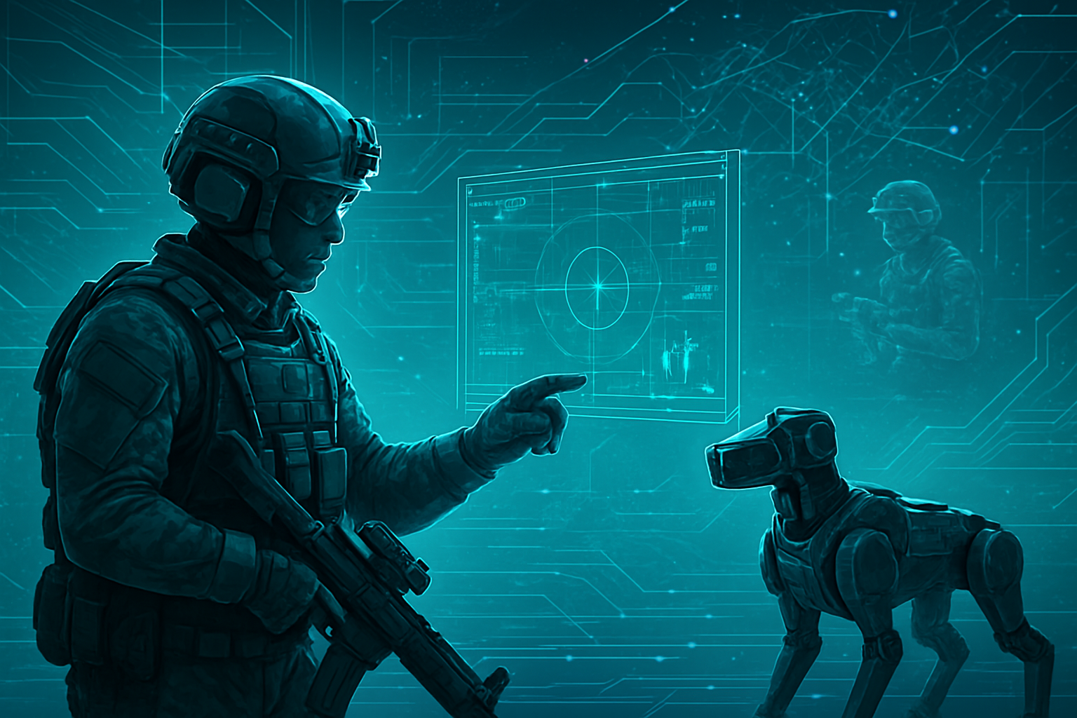
Immersive technologies like VR and AR provide unparalleled realism. VR transports soldiers into highly detailed digital terrains replicating urban battlegrounds or specific enemy installations for combat simulations, pilot training, and even medical scenarios. AR overlays digital information, such as enemy positions or navigation routes, directly onto a soldier's real-world view during live exercises, enhancing situational awareness. The integration of haptic feedback further enhances immersion, allowing for realistic physical sensations. These technologies significantly reduce the cost, logistical constraints, and risks associated with traditional field exercises, enabling more frequent, repeatable, and on-demand practice, leading to higher skill retention rates.
Data science is crucial for transforming raw data into actionable intelligence, improving military decision-making and logistics. Techniques like machine learning and predictive modeling process vast amounts of data from diverse sources—satellite imagery, sensor data, communication intercepts—to rapidly identify patterns, anomalies, and threats. This provides comprehensive situational awareness and helps optimize resource allocation and mission planning. Historically, military intelligence relied on slower, less integrated information processing. Data science now allows for real-time, data-driven decisions previously unimaginable, with the U.S. Army actively developing a specialized data science discipline to overcome "industrial age information management practices."
Finally, advanced cyber warfare training is paramount given the sophistication of digital threats. Cyber ranges, simulated risk-free environments mirroring real-world networks, allow personnel to practice offensive and defensive cyber operations, hone incident response, and test new technologies. These systems simulate a range of attacks, from espionage to AI/Machine Learning attacks. Specialized curricula cover cyberspace operations, protocol analysis, and intel integration, often culminating in immersive capstone events. This dedicated infrastructure and specialized training address the unique challenges of the digital battlefield, a domain largely absent from traditional military training.
Corporate Frontlines: How Tech Giants and Startups Are Adapting
The modernization of military training, with its increasing demand for essential tech skills, is creating a dynamic ecosystem that significantly impacts AI companies, tech giants, and startups alike. This push addresses the growing need for tech-savvy professionals, with veterans often possessing highly transferable skills like leadership, problem-solving, and experience with advanced systems.
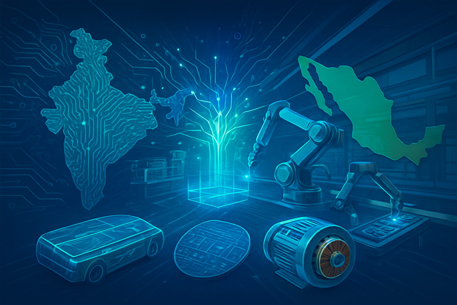
Several companies are poised to benefit immensely. In AI for defense, Palantir Technologies (NYSE: PLTR) is a significant player with its Gotham and Apollo software for intelligence integration and mission planning. Lockheed Martin (NYSE: LMT) integrates AI into platforms like the F-35 and develops AI tools through its Astris AI division. Anduril Industries (Private) focuses on autonomous battlefield systems with its Lattice AI platform. BigBear.ai (NYSE: BBAI) specializes in predictive military intelligence. Other key players include Northrop Grumman (NYSE: NOC), Raytheon Technologies (NYSE: RTX), and Shield AI.
For VR/AR/Simulation, InVeris (Firearms Training Systems – fats®) is a global leader, providing small-arms simulation and live-fire range solutions. Operator XR offers integrated, secure, and immersive VR systems for military training. Intellisense Systems develops VR/AR solutions for situational awareness, while BAE Systems (LSE: BAE) and VRAI collaborate on harnessing VR and AI for next-generation training. In data analytics, companies like DataWalk and GraphAware (Hume) provide specialized software for military intelligence. Tech giants such as Accenture (NYSE: ACN), IBM (NYSE: IBM), Microsoft (NASDAQ: MSFT), and Amazon Web Services (AWS) (NASDAQ: AMZN) also offer big data analytics solutions relevant to defense. The cybersecurity sector sees major players like Airbus (EURONEXT: AIR), Cisco (NASDAQ: CSCO), CrowdStrike (NASDAQ: CRWD), General Dynamics (NYSE: GD), and Palo Alto Networks (NASDAQ: PANW) implementing advanced security measures.
The competitive landscape is intensifying. While military tech training expands the talent pool, competition for skilled veterans, especially those with security clearances, is fierce. The defense sector is no longer a niche but a focal point for innovation, attracting significant venture capital. This pushes major AI labs and tech companies to align R&D with defense needs, focusing on robust AI solutions for mission-critical workflows. The development of "dual-use technologies"—innovations with both military and civilian applications—is becoming more prevalent, creating significant commercial spin-offs. This shift also accelerates the obsolescence of legacy systems, forcing traditional defense contractors to modernize their offerings, often by partnering with agile tech innovators.
Companies are gaining strategic advantages by actively recruiting military veterans, leveraging AI-driven skills-based hiring platforms, and focusing on dual-use technologies. Strategic partnerships with defense agencies and academic institutions are crucial for accelerating AI solution development. Emphasizing AI at the top of the tech stack, building custom AI systems for mission-critical areas, and establishing thought leadership in AI ethics and national security are also key. The Department of Defense's push for rapid prototyping and open architectures favors companies that can adapt quickly and integrate seamlessly.
Geopolitical Ramifications: AI, Ethics, and the Future of Conflict
The integration of AI into military training and operations carries profound societal and geopolitical consequences, reshaping global power dynamics and the very nature of warfare. AI is redefining geopolitical influence, with control over data, technology, and innovation becoming paramount, fueling a global AI arms race among major powers like the United States and China. This uneven adoption of AI technologies could significantly alter the global security landscape, potentially exacerbating existing asymmetries between nations.
A growing concern is the "civilianization" of warfare, where AI-controlled weapon systems developed outside conventional military procurement could become widely accessible, raising substantial ethical questions and potentially inducing a warlike bias within populations. Civilian tech firms are increasingly pivotal in military operations, providing AI tools for data analytics, drone strikes, and surveillance, blurring the lines between civilian and military tech and raising questions about their ethical and legal responsibilities during conflicts.
The most prominent ethical dilemma revolves around Lethal Autonomous Weapons Systems (LAWS) that can independently assess threats and make life-and-death decisions. Concerns include accountability for malfunctions, potential war crimes, algorithmic bias leading to disproportionate targeting, and the erosion of human judgment. The delegation of critical decisions to machines raises profound questions about human oversight and accountability, risking a "responsibility gap" where no human can be held accountable for the actions of autonomous systems. There's also a risk of over-reliance on AI, leading to a deskilling of human operators, and the "black box" nature of some AI systems, which lacks transparency for trust and risk analysis.
These advancements are viewed as a "seismic shift" in modeling and simulation, building upon past virtual trainers but making them far more robust and realistic. The global race to dominate AI is likened to past arms races, but broader, encompassing scientific, economic, and ideological influence. The potential impact of AI-enabled weapons is compared to the "Oppenheimer moment" of the 20th century, suggesting a fundamental redefinition of warfare akin to the introduction of nuclear weapons. This highlights that AI's integration is not merely an incremental technological improvement but a transformative breakthrough.
The absence of a comprehensive global governance framework for military AI is a critical regulatory gap, heightening risks to international peace and security and accelerating arms proliferation. AI acts as a "force multiplier," enhancing human capabilities in surveillance, logistics, targeting, and decision support, potentially leading to military operations with fewer human soldiers in high-risk environments. The civilian tech sector, as the primary driver of AI innovation, is intrinsically linked to military advancements, creating a complex relationship where private companies become pivotal actors in military operations. This intertwining underscores the urgent need for robust ethical frameworks and governance mechanisms that consider the dual-use nature of AI and the responsibilities of all stakeholders.
The Horizon of War: What Comes Next in Military Tech Training
The future of military training is set to be even more sophisticated, deeply integrated, and adaptive, driven by continuous technological advancements and the evolving demands of warfare. The overarching theme will be the creation of personalized, hyper-realistic, and multi-domain training environments, powered by next-generation AI and immersive technologies.
In the near term (next 1-5 years), AI will personalize training programs, adapting to individual learning styles and performance. Generative AI will revolutionize scenario development, automating resource-intensive processes and enabling the rapid creation of complex, dynamic scenarios for multi-domain and cyber warfare. Enhanced immersive simulations using VR, AR, and Extended Reality (XR) will become more prevalent, offering highly realistic and interconnected training environments for combat, tactical maneuvers, and decision-making. Initial training for human-machine teaming (HMT) will focus on fundamental interaction skills, teaching personnel to leverage the complementary strengths of humans and AI/autonomous machines. Cybersecurity and data management skills will become essential as reliance on interconnected systems grows.
Looking further ahead (beyond 5 years), next-generation AI, potentially including quantum computing, will lead to unprecedented training depth and efficiency. AI will process extensive datasets from multiple exercises, supporting the entire training spectrum from design to validation and accelerating soldier certification. Biometric data integration will monitor physical and mental states during training, further personalizing programs. Hyper-realistic and multi-domain Synthetic Training Environments (STEs) will seamlessly blend physical and virtual realities, incorporating haptic feedback and advanced sensory inputs to create simulations indistinguishable from real combat. Cross-branch and remote learning will be standard. Advanced HMT integration will focus on optimizing human-machine teaming at a cognitive level, fostering intuitive interaction and robust mental models between humans and AI. Training in quantum information sciences will also become vital.
Potential applications on the horizon include fully immersive combat simulations for urban warfare and counterterrorism, medical and trauma training with realistic emergency scenarios, advanced pilot and vehicle operator training, AR-guided maintenance and repair, and collaborative mission planning and rehearsal in 3D environments. Immersive simulations will also play a role in recruitment and retention by providing potential recruits with firsthand experiences.
However, significant challenges remain. The unprecedented pace of technological change demands continuous adaptation of training methodologies. Skill retention, especially for technical specialties, is a constant battle. The military will also have to compete with private industry for premier AI, machine learning, and robotics talent. Developing new doctrinal frameworks for emerging technologies like AI and HMT is critical, as there is currently no unified operational framework. Ensuring realism and concurrency in simulations, addressing the high cost of advanced facilities, and navigating the profound ethical dilemmas of AI, particularly autonomous weapon systems, are ongoing hurdles. Experts predict that mastering human-machine teaming will provide a critical advantage in future warfare, with the next two decades being more revolutionary in technological change than the last two. There will be an increased emphasis on using AI for strategic decision-making, challenging human biases, and recognizing patterns that humans might miss, while maintaining "meaningful human control" over lethal decisions.
The Unfolding Revolution: A Concluding Assessment
The ongoing convergence of military training and advanced technology signals a profound and irreversible shift in global defense paradigms. This era is defined by a relentless technological imperative, demanding that nations continuously invest in and integrate cutting-edge capabilities to secure national interests and maintain military superiority. The key takeaway is clear: future military strength will be intrinsically linked to technological prowess, with AI, immersive realities, and data science forming the bedrock of preparedness.
This development marks a critical juncture in AI history, showcasing its transition from theoretical exploration to practical, high-consequence application within the defense sector. The rigorous demands of military AI are pushing the boundaries of autonomous systems, advanced data processing, and human-AI teaming, setting precedents for ethical frameworks and responsible deployment that will likely influence other high-stakes industries globally. The defense sector's role as a significant driver of AI innovation will continue to shape the broader AI landscape.
The long-term impact will resonate across geopolitical dynamics and the very nature of warfare. Battlefields will be characterized by hybrid strategies, featuring advanced autonomous systems, swarm intelligence, and data-driven operations, often targeting critical infrastructure. This necessitates not only technologically proficient military personnel but also leaders capable of strategic thinking in highly dynamic, technologically saturated environments. Crucially, this technological imperative must be balanced with profound ethical considerations. The ethical and legal implications of AI in defense, particularly concerning lethal weapon systems, will remain central to international discourse, demanding principles of "meaningful human control," transparency, and accountability. The risk of automation bias and the dehumanization of warfare are serious concerns that require ongoing scrutiny.
In the coming weeks and months, watch for the accelerating adoption of generative AI for mission planning and predictive modeling. Keep an eye on new policy statements, international agreements, and national legislation addressing the responsible development and deployment of military AI. Continued investments and innovations in VR, AR, and synthetic training environments will be significant, as will advancements in cyber warfare capabilities and the integration of quantum encryption. Finally, track the growing trend of defense leveraging commercial technological innovations, particularly in robotics and autonomous systems, as startups and dual-use technologies drive rapid iteration and deployment. Successfully navigating this era will require not only technological prowess but also a steadfast commitment to ethical principles and a deep understanding of the human element in an increasingly automated world.
This content is intended for informational purposes only and represents analysis of current AI developments.
TokenRing AI delivers enterprise-grade solutions for multi-agent AI workflow orchestration, AI-powered development tools, and seamless remote collaboration platforms.
For more information, visit https://www.tokenring.ai/.