Tag: AI

  • Industrial Evolution: Boston Dynamics’ Electric Atlas Reports for Duty at Hyundai’s Georgia Metaplant

    Industrial Evolution: Boston Dynamics’ Electric Atlas Reports for Duty at Hyundai’s Georgia Metaplant

    In a landmark moment for the commercialization of humanoid robotics, Boston Dynamics has officially moved its all-electric Atlas robot from the laboratory to the factory floor. As of January 2026, the company—wholly owned by the Hyundai Motor Company (KRX: 005380)—has begun the industrial deployment of its next-generation humanoid at the Hyundai Motor Group Metaplant America (HMGMA) in Savannah, Georgia. This shift marks the transition of Atlas from a viral research sensation to a functional industrial asset, specialized for heavy lifting and autonomous parts sequencing within one of the world's most advanced automotive manufacturing hubs.

    The deployment centers on the "Software-Defined Factory" (SDF) philosophy, where hardware and software are seamlessly integrated to allow for rapid iteration and real-time optimization. At the HMGMA, Atlas is no longer performing the backflips that made its hydraulic predecessor famous; instead, it is tackling the "dull, dirty, and dangerous" tasks of a live production environment. By automating the movement of heavy components and organizing parts for human assembly lines, Hyundai aims to set a new global standard for the "Metaplant" of the future, leveraging what experts are calling "Physical AI."

    Precision Power: The Technical Architecture of the Electric Atlas

    The all-electric Atlas represents a radical departure from the hydraulic architecture that defined the platform for over a decade. While the previous model was a marvel of power density, its reliance on high-pressure pumps and hoses made it noisy, prone to leaks, and difficult to maintain in a sterile factory environment. The new 2026 production model utilizes custom-designed electric direct-drive actuators with a staggering torque density of 220 Nm/kg. This allows the robot to maintain a sustained payload capacity of 66 lbs (30 kg) and a burst-lift capability of up to 110 lbs (50 kg), comfortably handling the heavy engine components and battery modules typical of electric vehicle (EV) production.

    Technical specifications for the electric Atlas include 56 degrees of freedom—nearly triple that of the hydraulic version—and many of its joints are capable of full 360-degree rotation. This "superhuman" range of motion allows the robot to navigate cramped warehouse aisles by spinning its torso or limbs rather than turning its entire base, minimizing its footprint and increasing efficiency. Its perception system has been upgraded to a 360-degree sensor suite utilizing LiDAR and high-resolution cameras, processed locally by an onboard NVIDIA Corporation (NASDAQ: NVDA) Jetson Thor platform. This provides the robot with total spatial awareness, allowing it to operate safely alongside human workers without the need for safety cages.

    Initial reactions from the robotics community have been overwhelmingly positive, with researchers noting that the move to electric actuators simplifies the control stack significantly. Unlike previous approaches that required complex fluid dynamics modeling, the electric Atlas uses high-fidelity force control and tactile-sensing hands. This allows it to perform "blind" manipulations—sensing the weight and friction of an object through its fingertips—much like a human worker, which is critical for tasks like threading bolts or securing delicate wiring harnesses.

    The Humanoid Arms Race: Competitive and Strategic Implications

    The deployment at the Georgia Metaplant places Hyundai at the forefront of a burgeoning "Humanoid Arms Race," directly challenging the progress of Tesla (NASDAQ: TSLA) and its Optimus program. While Tesla has emphasized high-volume production and vertical integration, Hyundai’s strategy leverages the decades of R&D expertise from Boston Dynamics combined with one of the largest manufacturing footprints in the world. By treating the Georgia facility as a "live laboratory," Hyundai is effectively bypassing the simulation-to-reality gap that has slowed other competitors.

    This development is also a major win for the broader AI ecosystem. The electric Atlas’s "brain" is the result of collaboration between Boston Dynamics and Alphabet Inc. (NASDAQ: GOOGL) via its DeepMind unit, focusing on Large Behavior Models (LBM). These models enable the robot to handle "unstructured" environments—meaning it can figure out what to do if a parts bin is slightly out of place or if a component is dropped. This level of autonomy disrupts the traditional industrial robotics market, which has historically relied on fixed-path programming. Startups focusing on specialized robotic components, such as high-torque motors and haptic sensors, are likely to see increased investment as the demand for humanoid-scale parts scales toward mass production.

    Strategically, the HMGMA deployment serves as a blueprint for the "Robot Metaplant Application Center" (RMAC). This facility acts as a validation hub where manufacturing data is fed into Atlas’s AI models to ensure 99.9% reliability. By proving the technology in their own plants first, Hyundai and Boston Dynamics are positioning themselves to sell not just robots, but entire autonomous labor solutions to other industries, from aerospace to logistics.

    Physical AI and the Broader Landscape of Automation

    The integration of Atlas into the Georgia Metaplant is a milestone in the rise of "Physical AI"—the application of advanced machine learning to the physical world. For years, AI breakthroughs were largely confined to the digital realm, such as Large Language Models and image generation. However, the deployment of Atlas signifies that AI has matured enough to manage the complexities of gravity, friction, and multi-object interaction in real time. This move mirrors the "GPT-3 moment" for robotics, where the technology moves from an impressive curiosity to an essential tool for global industry.

    However, the shift is not without its concerns. The prospect of 30,000 humanoid units per year, as projected by Hyundai for the end of the decade, raises significant questions regarding the future of the manufacturing workforce. While Hyundai maintains that Atlas is designed to augment human labor by taking over the most strenuous tasks, labor economists warn of potential displacement in traditional assembly roles. The broader significance lies in how society will adapt to a world where "general-purpose" robots can be retrained for new tasks overnight simply by downloading a new software update, much like a smartphone app.

    Compared to previous milestones, such as the first deployment of UNIMATE in the 1960s, the Atlas rollout is uniquely collaborative. The use of "Digital Twins" allows engineers in South Korea to simulate tasks in a virtual environment before "pushing" the code to robots in Georgia. This global, cloud-based approach to labor is a fundamental shift in how manufacturing is conceptualized, turning a physical factory into a programmable asset.

    The Road Ahead: From Parts Sequencing to Full Assembly

    In the near term, we can expect the fleet of Atlas robots at the HMGMA to expand from a handful of pilot units to a full-scale workforce. The immediate focus remains on parts sequencing and material handling, but the roadmap for 2027 and 2028 includes more complex assembly tasks. These will include the installation of interior trim and the routing of EV cooling systems—tasks that require the high dexterity and fine motor skills that Boston Dynamics is currently refining in the RMAC.

    Looking further ahead, the goal is for Atlas to reach a state of "unsupervised autonomy," where it can self-diagnose mechanical issues and navigate to autonomous battery-swapping stations without human intervention. The challenges remaining are significant, particularly in the realm of long-term durability and the energy density of batteries required for a full 8-hour shift of heavy lifting. However, experts predict that as the "Software-Defined Factory" matures, the hardware will become increasingly modular, allowing for "hot-swapping" of limbs or sensors in minutes rather than hours.

    A New Chapter in Robotics History

    The deployment of the all-electric Atlas at Hyundai’s Georgia Metaplant is more than just a corporate milestone; it is a signal that the era of the general-purpose humanoid has arrived. By moving beyond the hydraulic prototypes of the past and embracing a software-first, all-electric architecture, Boston Dynamics and Hyundai have successfully bridged the gap between a high-tech demo and an industrial workhorse.

    The coming months will be critical as the HMGMA scales its production of EVs and its integration of robotic labor. Observers should watch for the reliability metrics coming out of the Savannah facility and the potential for Boston Dynamics to announce third-party pilot programs with other industrial giants. While the backflips may be over, the real work for Atlas—and the future of the global manufacturing sector—has only just begun.


    This content is intended for informational purposes only and represents analysis of current AI developments.

    TokenRing AI delivers enterprise-grade solutions for multi-agent AI workflow orchestration, AI-powered development tools, and seamless remote collaboration platforms.
    For more information, visit https://www.tokenring.ai/.

  • The Open-Source Renaissance: RISC-V Dismantles ARM’s Hegemony in Data Centers and Connected Cars

    The Open-Source Renaissance: RISC-V Dismantles ARM’s Hegemony in Data Centers and Connected Cars

    As of January 21, 2026, the global semiconductor landscape has reached a historic inflection point. Long considered a niche experimental architecture for microcontrollers and academic research, RISC-V has officially transitioned into a high-performance powerhouse, aggressively seizing market share from Arm Holdings (NASDAQ: ARM) in the lucrative data center and automotive sectors. The shift is driven by a unique combination of royalty-free licensing, unprecedented customization capabilities, and a geopolitical push for "silicon sovereignty" that has united tech giants and startups alike.

    The arrival of 2026 has seen the "Great Migration" gather pace. No longer just a cost-saving measure, RISC-V is now the architecture of choice for specialized AI workloads and Software-Defined Vehicles (SDVs). With major silicon providers and hyperscalers seeking to escape the "ARM tax" and restrictive licensing agreements, the open-standard architecture is now integrated into over 25% of all new chip designs. This development represents the most significant challenge to proprietary instruction set architectures (ISAs) since the rise of x86, signaling a new era of decentralized hardware innovation.

    The Performance Parity Breakthrough

    The technical barrier that once kept RISC-V out of the server room has been shattered. The ratification of the RVA23 profile in late 2024 provided the industry with a mandatory baseline for 64-bit application processors, standardizing critical features such as hypervisor extensions for virtualization and advanced vector processing. In early 2026, benchmarks for the Ventana Veyron V2 and Tenstorrent’s Ascalon-D8 have shown that RISC-V "brawny" cores have finally reached performance parity with ARM’s Neoverse V2 and V3. These chips, manufactured on leading-edge 4nm and 3nm nodes, feature 15-wide out-of-order pipelines and clock speeds exceeding 3.8 GHz, proving that open-source designs can match the raw single-threaded performance of the world’s most advanced proprietary cores.

    Perhaps the most significant technical advantage of RISC-V in 2026 is its "Vector-Length Agnostic" (VLA) nature. Unlike the fixed-width SIMD instructions in ARM’s NEON or the complex implementation of SVE2, RISC-V Vector (RVV) 1.0 and 2.0 allow developers to write code that scales across any hardware width, from 128-bit mobile chips to 512-bit AI accelerators. This flexibility is augmented by the new Integrated Matrix Extension (IME), which allows processors to perform dense matrix-matrix multiplications—the core of Large Language Model (LLM) inference—directly within the CPU’s register file. This minimizes "context switch" overhead and provides a 30-40% improvement in performance-per-watt for AI workloads compared to general-purpose ARM designs.

    Industry experts and the research community have reacted with overwhelming support. The RACE (RISC-V AI Computability Ecosystem) initiative has successfully closed the "software gap," delivering zero-day support for major frameworks like PyTorch and JAX on RVA23-compliant silicon. Dr. David Patterson, a pioneer of RISC and Vice-Chair of RISC-V International, noted that the modularity of the architecture allows companies to strip away legacy "cruft," creating leaner, more efficient silicon that is purpose-built for the AI era rather than being retrofitted for it.

    The "Gang of Five" and the Qualcomm Gambit

    The corporate landscape was fundamentally reshaped in December 2025 when Qualcomm (NASDAQ: QCOM) announced the acquisition of Ventana Micro Systems. This move, described by analysts as a "declaration of independence," gives Qualcomm a sovereign high-performance CPU roadmap, allowing it to bypass the ongoing legal and financial frictions with Arm Holdings (NASDAQ: ARM). By integrating Ventana’s Veyron technology into its future server and automotive platforms, Qualcomm is no longer just a licensee; it is a primary architect of its own destiny, a move that has sent ripples through the valuations of proprietary IP providers.

    In the automotive sector, the "Gang of Five"—a joint venture known as Quintauris involving Bosch, Qualcomm, Infineon, Nordic, and NXP—reached a critical milestone this month with the release of the RT-Europa Platform. This standardized RISC-V real-time platform is designed to power the next generation of autonomous driving and cockpit systems. Meanwhile, Mobileye, an Intel (NASDAQ: INTC) company, is already shipping its EyeQ6 and EyeQ Ultra chips in volume. These Level 4 autonomous driving platforms utilize a cluster of 12 high-performance RISC-V cores, proving that the architecture can meet the most stringent ISO 26262 functional safety requirements for mass-market vehicles.

    Hyperscalers are also leading the charge. Alphabet Inc. (NASDAQ: GOOGL) and Meta (NASDAQ: META) have expanded their RISC-V deployments to manage internal AI infrastructure and video processing. A notable development in 2026 is the collaboration between SiFive and NVIDIA (NASDAQ: NVDA), which allows for the integration of NVLink Fusion into RISC-V compute platforms. This enables cloud providers to build custom AI servers where open-source RISC-V CPUs orchestrate clusters of NVIDIA GPUs with coherent, high-bandwidth connectivity, effectively commoditizing the CPU portion of the AI server stack.

    Sovereignty, Geopolitics, and the Open Standard

    The ascent of RISC-V is as much a geopolitical story as a technical one. In an era of increasing trade restrictions and "tech-nationalism," the royalty-free and open nature of RISC-V has made it a centerpiece of national strategy. For the European Union and major Asian economies, the architecture offers a way to build a domestic semiconductor industry that is immune to foreign licensing freezes or sudden shifts in the corporate strategy of a single UK- or US-based entity. This "silicon sovereignty" has led to massive public-private investments, particularly in the EuroHPC JU project, which aims to power Europe’s next generation of exascale supercomputers with RISC-V.

    Comparisons are frequently drawn to the rise of Linux in the 1990s. Just as Linux broke the stranglehold of proprietary operating systems in the server market, RISC-V is doing the same for the hardware layer. By removing the "gatekeeper" model of traditional ISA licensing, RISC-V enables a more democratic form of innovation where a startup in Bangalore can contribute to the same ecosystem as a tech giant in Silicon Valley. This collaboration has accelerated the pace of development, with the RISC-V community achieving in five years what took proprietary architectures decades to refine.

    However, this rapid growth has not been without concerns. Regulatory bodies in the United States and Europe are closely monitoring the security implications of open-source hardware. While the transparency of RISC-V allows for more rigorous auditing of hardware-level vulnerabilities, the ease with which customized extensions can be added has raised questions about fragmentation and "hidden" features. To combat this, RISC-V International has doubled down on its compliance and certification programs, ensuring that the "Open-Source Renaissance" does not lead to a fragmented "Balkanization" of the hardware world.

    The Road to 2nm and Beyond

    Looking toward the latter half of 2026 and 2027, the roadmap for RISC-V is increasingly ambitious. Tenstorrent has already teased its "Callandor" core, targeting a staggering 35 SPECint/GHz, which would position it as the world’s fastest CPU core regardless of architecture. We expect to see the first production vehicles utilizing the Quintauris RT-Europa platform hit the roads by mid-2027, marking the first time that the entire "brain" of a mass-market car is powered by an open-standard ISA.

    The next frontier for RISC-V is the 2nm manufacturing node. As the costs of designing chips on such advanced processes skyrocket, the ability to save millions in licensing fees becomes even more attractive to smaller players. Furthermore, the integration of RISC-V into the "Chiplet" ecosystem is expected to accelerate. We anticipate a surge in "heterogeneous" packages where a RISC-V management processor sits alongside specialized AI accelerators and high-speed I/O tiles, all connected via the Universal Chiplet Interconnect Express (UCIe) standard.

    A New Pillar of Modern Computing

    The growth of RISC-V in the automotive and data center sectors is no longer a "potential" threat to the status quo; it is an established reality. The architecture has proven it can handle the most demanding workloads on earth, from managing exabytes of data in the cloud to making split-second safety decisions in autonomous vehicles. In the history of artificial intelligence and computing, January 2026 will likely be remembered as the moment the industry collectively decided that the foundation of our digital future must be open, transparent, and royalty-free.

    The key takeaway for the coming months is the shift in focus from "can it work?" to "how fast can we deploy it?" As the RVA23 profile matures and more "plug-and-play" RISC-V IP becomes available, the cost of entry for custom silicon will continue to fall. Watch for Arm Holdings (NASDAQ: ARM) to pivot its business model even further toward high-end, vertically integrated system-on-chips (SoCs) to defend its remaining moats, and keep a close eye on the performance of the first batch of RISC-V-powered AI servers entering the public cloud. The hardware revolution is here, and it is open-source.


    This content is intended for informational purposes only and represents analysis of current AI developments.

    TokenRing AI delivers enterprise-grade solutions for multi-agent AI workflow orchestration, AI-powered development tools, and seamless remote collaboration platforms.
    For more information, visit https://www.tokenring.ai/.
  • The Silicon Supercycle: Semiconductor Industry Poised to Shatter $1 Trillion Milestone in 2026

    The Silicon Supercycle: Semiconductor Industry Poised to Shatter $1 Trillion Milestone in 2026

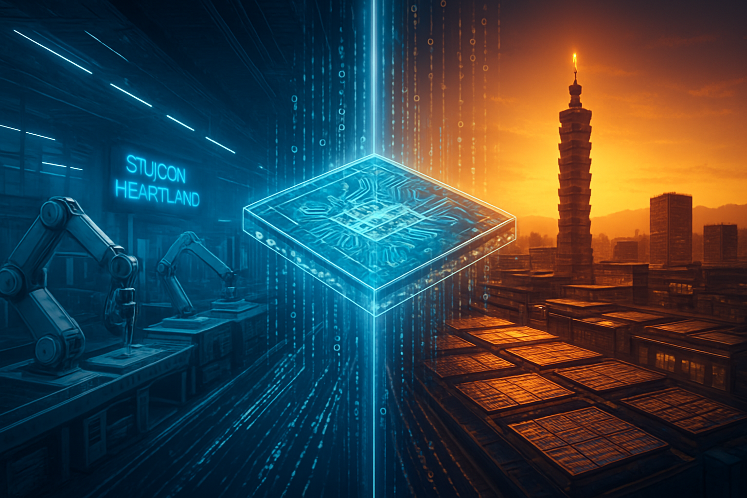
    As of January 21, 2026, the global semiconductor industry stands on the precipice of a historic achievement: the $1 trillion annual revenue milestone. Long predicted by analysts to occur at the end of the decade, this monumental valuation has been pulled forward by nearly four years due to a "Silicon Supercycle" fueled by the insatiable demand for generative AI infrastructure and the rapid evolution of High Bandwidth Memory (HBM).

    This acceleration marks a fundamental shift in the global economy, transitioning the semiconductor sector from a cyclical industry prone to "boom and bust" periods in PCs and smartphones into a structural growth engine for the artificial intelligence era. With the industry crossing the $975 billion mark at the close of 2025, current Q1 2026 data indicates that the trillion-dollar threshold will be breached by mid-year, driven by a new generation of AI accelerators and advanced memory architectures.

    The Technical Engine: HBM4 and the 2048-bit Breakthrough

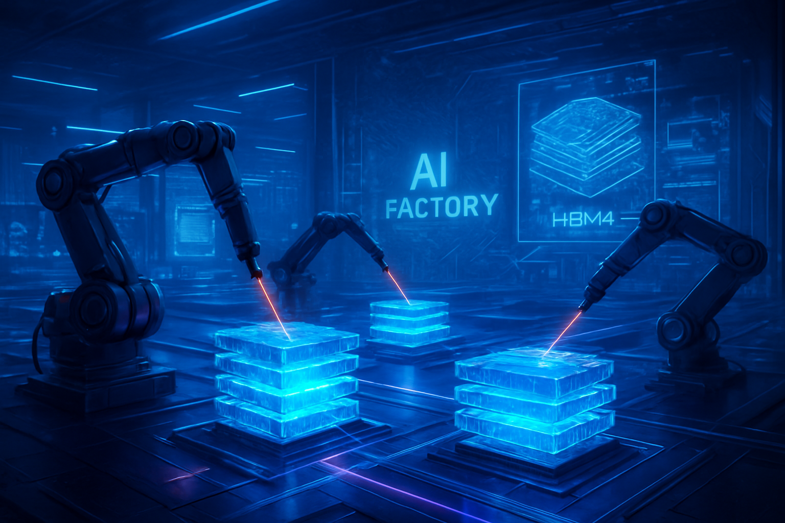
    The primary technical catalyst for this growth is the desperate need to overcome the "Memory Wall"—the bottleneck where data processing speeds outpace the ability of memory to feed that data to the processor. In 2026, the transition from HBM3e to HBM4 has become the industry's most significant technical leap. Unlike previous iterations, HBM4 doubles the interface width from a 1024-bit bus to a 2048-bit bus, providing bandwidth exceeding 2.0 TB/s per stack. This allows the latest AI models, which now routinely exceed several trillion parameters, to operate with significantly reduced latency.

    Furthermore, the manufacturing of these memory stacks has fundamentally changed. For the first time, the "base logic die" at the bottom of the HBM stack is being manufactured on advanced logic nodes, such as the 5nm process from TSMC (NYSE: TSM), rather than traditional DRAM nodes. This hybrid approach allows for much higher efficiency and closer integration with GPUs. To manage the extreme heat generated by these 16-hi and 20-hi stacks, the industry has widely adopted "Hybrid Bonding" (copper-to-copper), which replaces traditional microbumps and allows for thinner, more thermally efficient chips.

    Initial reactions from the AI research community have been overwhelmingly positive, as these hardware gains are directly translating to a 3x to 5x improvement in training efficiency for next-generation large multimodal models (LMMs). Industry experts note that without the 2026 deployment of HBM4, the scaling laws of AI would have likely plateaued due to energy constraints and data transfer limitations.

    The Market Hierarchy: Nvidia and the Memory Triad

    The drive toward $1 trillion has reshaped the corporate leaderboard. Nvidia (NASDAQ: NVDA) continues its reign as the world’s most valuable semiconductor company, having become the first chip designer to surpass $125 billion in annual revenue. Their dominance is currently anchored by the Blackwell Ultra and the newly launched Rubin architecture, which utilizes advanced HBM4 modules to maintain a nearly 90% share of the AI data center market.

    In the memory sector, a fierce "triad" has emerged between SK Hynix (KRX: 000660), Samsung Electronics (KRX: 005930), and Micron Technology (NASDAQ: MU). SK Hynix currently maintains a slim lead in HBM market share, but Samsung has gained significant ground in early 2026 by leveraging its "turnkey" model—offering memory, foundry, and advanced packaging under one roof. Micron has successfully carved out a high-margin niche by focusing on power-efficient HBM3e for edge-AI devices, which are now beginning to see mass adoption in the enterprise laptop and smartphone markets.

    This shift has left legacy players like Intel (NASDAQ: INTC) in a challenging position, as they race to pivot their manufacturing capabilities toward the advanced packaging services (like CoWoS-equivalent technologies) that AI giants demand. The competitive landscape is no longer just about who has the fastest processor, but who can secure the most capacity on TSMC’s 2nm and 3nm production lines.

    The Wider Significance: A Structural Shift in Global Compute

    The significance of the $1 trillion milestone extends far beyond corporate balance sheets. It represents a paradigm shift where the "compute intensity" of the global economy has reached a tipping point. In previous decades, the semiconductor market was driven by consumer discretionary spending on gadgets; today, it is driven by sovereign AI initiatives and massive capital expenditure from "Hyperscalers" like Microsoft, Google, and Meta.

    However, this rapid growth has raised significant concerns regarding power consumption and supply chain fragility. The concentration of advanced manufacturing in East Asia remains a geopolitical flashpoint, even as the U.S. and Europe bring more "fab" capacity online via the CHIPS Act. Furthermore, the sheer energy required to run the HBM-heavy data centers needed for the $1 trillion market is forcing a secondary boom in power semiconductors and "green" data center infrastructure.

    Comparatively, this milestone is being viewed as the "Internet Moment" for hardware. Just as the build-out of fiber optic cables in the late 1990s laid the groundwork for the digital economy, the current build-out of AI infrastructure is seen as the foundational layer for the next fifty years of autonomous systems, drug discovery, and climate modeling.

    Future Horizons: Beyond HBM4 and Silicon Photonics

    Looking ahead to the remainder of 2026 and into 2027, the industry is already preparing for the next frontier: Silicon Photonics. As traditional electrical interconnects reach their physical limits, the industry is moving toward optical interconnects—using light instead of electricity to move data between chips. This transition is expected to further reduce power consumption and allow for even larger clusters of GPUs to act as a single, massive "super-chip."

    In the near term, we expect to see "Custom HBM" become the norm, where AI companies like OpenAI or Amazon design their own logic layers for memory stacks, tailored specifically to their proprietary algorithms. The challenge remains the yield rates of these incredibly complex 3D-stacked components; as chips become taller and more integrated, a single defect can render a very expensive component useless.

    The Road to $1 Trillion and Beyond

    The semiconductor industry's journey to $1 trillion in 2026 is a testament to the accelerating pace of human innovation. What was once a 2030 goal was reached four years early, catalyzed by the sudden and profound emergence of generative AI. The key takeaways from this milestone are clear: memory is now as vital as compute, advanced packaging is the new battlefield, and the semiconductor industry is now the undisputed backbone of global geopolitics and economics.

    As we move through 2026, the industry's focus will likely shift from pure capacity expansion to efficiency and sustainability. The "Silicon Supercycle" shows no signs of slowing down, but its long-term success will depend on how well the industry can manage the environmental and geopolitical pressures that come with being a trillion-dollar titan. In the coming months, keep a close eye on the rollout of Nvidia’s Rubin chips and the first shipments of mass-produced HBM4; these will be the bellwethers for the industry's next chapter.


    This content is intended for informational purposes only and represents analysis of current AI developments.

    TokenRing AI delivers enterprise-grade solutions for multi-agent AI workflow orchestration, AI-powered development tools, and seamless remote collaboration platforms.
    For more information, visit https://www.tokenring.ai/.

  • The Speed of Light: Silicon Photonics and CPO Emerge as the Backbone of the ‘Million-GPU’ AI Power Grid

    The Speed of Light: Silicon Photonics and CPO Emerge as the Backbone of the ‘Million-GPU’ AI Power Grid

    As of January 2026, the artificial intelligence industry has reached a pivotal physical threshold. For years, the scaling of large language models was limited by compute density and memory capacity. Today, however, the primary bottleneck has shifted to the "Energy Wall"—the staggering amount of power required simply to move data between processors. To shatter this barrier, the semiconductor industry is undergoing its most significant architectural shift in a decade: the transition from copper-based electrical signaling to light-based interconnects. Silicon Photonics and Co-Packaged Optics (CPO) are no longer experimental concepts; they have become the critical infrastructure, or the "backbone," of the modern AI power grid.

    The significance of this transition cannot be overstated. As hyperscalers race toward building "million-GPU" clusters to train the next generation of Artificial General Intelligence (AGI), the traditional "I/O tax"—the energy consumed by data moving across a data center—has threatened to stall progress. By integrating optical engines directly onto the chip package, companies are now able to reduce data-transfer energy consumption by up to 70%, effectively redirecting megawatts of power back into actual computation. This month marks a major milestone in this journey, as the industry’s biggest players, including TSMC (NYSE: TSM), Broadcom (NASDAQ: AVGO), and Ayar Labs, unveil the production-ready hardware that will define the AI landscape for the next five years.

    Breaking the Copper Wall: Technical Foundations of 2026

    The technical heart of this revolution lies in the move from pluggable transceivers to Co-Packaged Optics. Leading the charge is Taiwan Semiconductor Manufacturing Company (TPE: 2330), whose Compact Universal Photonic Engine (COUPE) technology has entered its final production validation phase this January, with full-scale mass production slated for the second half of 2026. COUPE utilizes TSMC’s proprietary SoIC-X (System on Integrated Chips) 3D-stacking technology to place an Electronic Integrated Circuit (EIC) directly on top of a Photonic Integrated Circuit (PIC). This configuration eliminates the parasitic capacitance of traditional wiring, supporting staggering bandwidths of 1.6 Tbps in its first generation, with a roadmap toward 12.8 Tbps by 2028.

    Simultaneously, Broadcom (NASDAQ: AVGO) has begun shipping pilot units of its Gen 3 CPO platform, powered by the Tomahawk 6 (code-named "Davisson") switch silicon. This generation introduces 200 Gbps per lane optical connectivity, enabling the construction of 102.4 Tbps Ethernet switches. Unlike previous iterations, Broadcom’s Gen 3 removes the power-hungry Digital Signal Processor (DSP) from the optical module, utilizing a "direct drive" architecture that slashes latency to under 10 nanoseconds. This is critical for the "scale-up" fabrics required by NVIDIA (NASDAQ: NVDA) and AMD (NASDAQ: AMD), where thousands of GPUs must act as a single, massive processor without the lag inherent in traditional networking.

    Further diversifying the ecosystem is the partnership between Ayar Labs and Global Unichip Corp (TPE: 3443). The duo has successfully integrated Ayar Labs’ TeraPHY™ optical engines into GUC’s advanced ASIC design workflow. Using the Universal Chiplet Interconnect Express (UCIe) standard, they have achieved a "shoreline density" of 1.4 Tbps/mm², allowing more than 100 Tbps of aggregate bandwidth from a single processor package. This approach solves the mechanical and thermal challenges of CPO by using specialized "stiffener" designs and detachable fiber connectors, making light-based I/O accessible for custom AI accelerators beyond just the major GPU vendors.

    A New Competitive Frontier for Hyperscalers and Chipmakers

    The shift to silicon photonics creates a clear divide between those who can master light-based interconnects and those who cannot. For major AI labs and hyperscalers like Google (NASDAQ: GOOGL) and Meta (NASDAQ: META), this technology is the "buy" that allows them to scale their data centers from single buildings to entire "AI Factories." By reducing the "I/O tax" from 20 picojoules per bit (pJ/bit) to less than 5 pJ/bit, these companies can operate much larger clusters within the same power envelope, providing a massive strategic advantage in the race for AGI.

    NVIDIA and AMD are the most immediate beneficiaries. NVIDIA is already preparing its "Rubin Ultra" platform to integrate TSMC’s COUPE technology, ensuring its leadership in the "scale-up" domain where low-latency communication is king. Meanwhile, Broadcom’s dominance in the networking fabric allows it to act as the primary "toll booth" for the AI power grid. For startups, the Ayar Labs and GUC partnership is a game-changer; it provides a standardized, validated path to integrate optical I/O into bespoke AI silicon, potentially disrupting the dominance of off-the-shelf GPUs by allowing specialized chips to communicate at speeds previously reserved for top-tier hardware.

    However, this transition is not without risk. The move to CPO disrupts the traditional "pluggable" optics market, long dominated by specialized module makers. As optical engines move onto the chip package, the traditional supply chain is being compressed, forcing many optics companies to either partner with foundries or face obsolescence. The market positioning of TSMC as a "one-stop shop" for both logic and photonics packaging further consolidates power in the hands of the world's largest foundry, raising questions about future supply chain resilience.

    Lighting the Way to AGI: Wider Significance

    The rise of silicon photonics represents more than just a faster way to move data; it is a fundamental shift in the AI landscape. In the era of the "Copper Wall," physical distance was a dealbreaker—high-speed electrical signals could only travel about a meter before degrading. This limited AI clusters to single racks or small rows. Silicon photonics extends that reach to over 100 meters without significant signal loss. This enables the "million-GPU" vision where a "scale-up" domain can span an entire data hall, allowing models to be trained on datasets and at scales that were previously physically impossible.

    Comparatively, this milestone is as significant as the transition from HDD to SSD or the move to FinFET transistors. It addresses the sustainability crisis currently facing the tech industry. As data centers consume an ever-increasing percentage of global electricity, the 70% energy reduction offered by CPO is a critical "green" technology. Without it, the environmental and economic cost of training models like GPT-6 or its successors would likely have become prohibitive, potentially triggering an "AI winter" driven by resource constraints rather than lack of algorithmic progress.

    However, concerns remain regarding the reliability of laser sources. Unlike electronic components, lasers have a finite lifespan and are sensitive to the high heat generated by AI processors. The industry is currently split between "internal" lasers integrated into the package and "External Laser Sources" (ELS) that can be swapped out like a lightbulb. How the industry settles this debate in 2026 will determine the long-term maintainability of the world's most expensive compute clusters.

    The Horizon: From 1.6T to 12.8T and Beyond

    Looking ahead to the remainder of 2026 and into 2027, the focus will shift from "can we do it" to "can we scale it." Following the H2 2026 mass production of first-gen COUPE, experts predict an immediate push toward the 6.4 Tbps generation. This will likely involve even tighter integration with CoWoS (Chip-on-Wafer-on-Substrate) packaging, effectively blurring the line between the processor and the network. We expect to see the first "All-Optical" AI data center prototypes emerge by late 2026, where even the memory-to-processor links utilize silicon photonics.

    Near-term developments will also focus on the standardization of the "optical chiplet." With UCIe-S and UCIe-A standards gaining traction, we may see a marketplace where companies can mix and match logic chiplets from one vendor with optical chiplets from another. The ultimate goal is "Optical I/O for everything," extending from the high-end GPU down to consumer-grade AI PCs and edge devices, though those applications remain several years away. Challenges like fiber-attach automation and high-volume testing of photonic circuits must be addressed to bring costs down to the level of traditional copper.

    Summary and Final Thoughts

    The emergence of Silicon Photonics and Co-Packaged Optics as the backbone of the AI power grid marks the end of the "Copper Age" of computing. By leveraging the speed and efficiency of light, TSMC, Broadcom, Ayar Labs, and their partners have provided the industry with a way over the "Energy Wall." With TSMC’s COUPE entering mass production in H2 2026 and Broadcom’s Gen 3 CPO already in the hands of hyperscalers, the infrastructure for the next generation of AI is being laid today.

    In the history of AI, this will likely be remembered as the moment when physical hardware caught up to the ambitions of software. The transition to light-based interconnects ensures that the scaling laws which have driven AI progress so far can continue for at least another decade. In the coming weeks and months, all eyes will be on the first deployment data from Broadcom’s Tomahawk 6 pilots and the final yield reports from TSMC’s COUPE validation lines. The era of the "Million-GPU" cluster has officially begun, and it is powered by light.


    This content is intended for informational purposes only and represents analysis of current AI developments.

    TokenRing AI delivers enterprise-grade solutions for multi-agent AI workflow orchestration, AI-powered development tools, and seamless remote collaboration platforms.
    For more information, visit https://www.tokenring.ai/.
  • The RISC-V Revolution: How Open Architecture Conquered the AI Landscape in 2026

    The RISC-V Revolution: How Open Architecture Conquered the AI Landscape in 2026

    The long-heralded "third pillar" of computing has officially arrived. As of January 2026, the semiconductor industry is witnessing a seismic shift as RISC-V, the open-source instruction set architecture (ISA), transitions from a niche academic project to a dominant force in the global AI infrastructure. Driven by a desire for "technological sovereignty" and the need to bypass increasingly expensive proprietary licenses, the world's largest tech entities and geopolitical blocs are betting their silicon futures on open standards.

    The numbers tell a story of rapid, uncompromising adoption. NVIDIA (NASDAQ: NVDA) recently confirmed it has surpassed a cumulative milestone of shipping over one billion RISC-V cores across its product stack, while the European Union has doubled down on its commitment to independence with a fresh €270 million investment into the RISC-V ecosystem. This surge represents more than just a change in technical specifications; it marks a fundamental redistribution of power in the global tech economy, challenging the decades-long duopoly of x86 and ARM (NASDAQ: ARM).

    The Technical Ascent: From Microcontrollers to Exascale Engines

    The technical narrative of RISC-V in early 2026 is defined by its graduation from simple management tasks to high-performance AI orchestration. While NVIDIA has historically used RISC-V for its internal "Falcon" microcontrollers, the latest Rubin GPU architecture, unveiled this month, utilizes custom NV-RISCV cores to manage everything from secure boot and power regulation to complex NVLink-C2C (Chip-to-Chip) memory coherency. By integrating up to 40 RISC-V cores per chip, NVIDIA has essentially created a "shadow" processing layer that handles the administrative heavy lifting, freeing up its proprietary CUDA cores for pure AI computation.

    Perhaps the most significant technical breakthrough of the year is the integration of NVIDIA NVLink Fusion into SiFive’s high-performance compute platforms. For the first time, a non-proprietary RISC-V CPU can connect directly to NVIDIA’s state-of-the-art GPUs with 3.6 TB/s of bandwidth. This level of hardware interoperability was previously reserved for NVIDIA’s own ARM-based Grace and Vera CPUs. Meanwhile, Jim Keller’s Tenstorrent has successfully productized its TT-Ascalon RISC-V core, which benchmarks from January 2026 show achieving performance parity with Intel’s (NASDAQ: INTC) Zen 5 and ARM’s Neoverse V3 in integer workloads.

    This modularity is RISC-V's "secret weapon." Unlike the rigid, licensed designs of x86 or ARM, RISC-V allows architects to add custom "extensions" specifically designed for AI math—such as matrix multiplication or vector processing—without seeking permission from a central authority. This flexibility has allowed startups like Axelera AI and MIPS to launch specialized Neural Processing Units (NPUs) that offer a 30% to 40% improvement in Performance-Power-Area (PPA) compared to traditional, general-purpose chips.

    The Business of Sovereignty: Tech Giants and Geopolitics

    The shift toward RISC-V is as much about balance sheets as it is about transistors. For companies like NVIDIA and Qualcomm (NASDAQ: QCOM), the adoption of RISC-V serves as a strategic hedge against the "ARM tax"—the rising licensing fees and restrictive terms that have defined the ARM ecosystem in recent years. Qualcomm’s pivot toward RISC-V for its "Snapdragon Data Center" platforms, following its acquisition of RISC-V assets in late 2025, signals a clear move to reclaim control over its long-term roadmap.

    In the cloud, the impact is even more pronounced. Hyperscalers such as Meta (NASDAQ: META) and Alphabet (NASDAQ: GOOGL) are increasingly utilizing RISC-V for the control logic within their custom AI accelerators (MTIA and TPU). By treating the instruction set as a "shared public utility" rather than a proprietary product, these companies can collaborate on foundational software—like Linux kernels and compilers—while competing on the proprietary hardware logic they build on top. This "co-opetition" model has accelerated the maturity of the RISC-V software stack, which was once considered its greatest weakness.

    Furthermore, the recent acquisition of Synopsys’ ARC-V processor line by GlobalFoundries (NASDAQ: GFS) highlights a consolidation of the ecosystem. Foundries are no longer just manufacturing chips; they are providing the open-source IP necessary for their customers to design them. This vertical integration is making it easier for smaller AI startups to bring custom silicon to market, disrupting the traditional "one-size-fits-all" hardware model that dominated the previous decade.

    A Geopolitical Fortress: Europe’s Quest for Digital Autonomy

    The surge in RISC-V adoption is inextricably linked to the global drive for "technological sovereignty." Nowhere is this more apparent than in the European Union, where the DARE (Digital Autonomy for RISC-V in Europe) project has received a massive €270 million boost. Coordinated by the Barcelona Supercomputing Center, DARE aims to ensure that the next generation of European exascale supercomputers and automotive systems are built on homegrown hardware, free from the export controls and geopolitical whims of foreign powers.

    By January 2026, the DARE project has reached a critical milestone: the successful tape-out of three specialized chiplets: a Vector Accelerator (VEC), an AI Processing Unit (AIPU), and a General-Purpose Processor (GPP). These chiplets are designed to be "Lego-like" components that European manufacturers can mix and match to build everything from autonomous vehicle controllers to energy-efficient data centers. This "silicon-to-software" independence is viewed by EU regulators as essential for economic security in an era where AI compute has become the world’s most valuable resource.

    The broader significance of this movement cannot be overstated. Much like how Linux democratized the world of software and the internet, RISC-V is democratizing the world of hardware. It represents a shift from a world of "black box" processors to a transparent, auditable architecture. For industries like defense, aerospace, and finance, the ability to verify every instruction at the hardware level is a massive security advantage over proprietary designs that may contain undocumented features or vulnerabilities.

    The Road Ahead: Consumer Integration and Challenges

    Looking toward the remainder of 2026 and beyond, the next frontier for RISC-V is the consumer market. At CES 2026, Tenstorrent and Razer announced a modular AI accelerator for laptops that connects via Thunderbolt, allowing developers to run massive Large Language Models (LLMs) locally. This is just the beginning; as the software ecosystem continues to stabilize, experts predict that RISC-V will begin appearing as the primary processor in high-end smartphones and AI PCs by 2027.

    However, challenges remain. While the hardware is ready, the "software gap" is still being bridged. While Linux and major AI frameworks like PyTorch and TensorFlow run well on RISC-V, thousands of legacy enterprise applications still require x86 or ARM. Bridging this gap through high-performance binary translation—similar to Apple's Rosetta 2—will be a key focus for the developer community in the coming months. Additionally, as more companies add their own custom extensions to the base RISC-V ISA, the risk of "fragmentation"—where chips become too specialized to share common software—is a concern that the RISC-V International foundation is working hard to mitigate.

    The Dawn of the Open Silicon Era

    The events of early 2026 mark a definitive turning point in computing history. NVIDIA’s shipment of one billion cores and the EU’s strategic multi-million euro investments have proven that RISC-V is no longer a "future" technology—it is the architecture of the present. By decoupling the hardware instruction set from the corporate interests of a single entity, the industry has unlocked a new level of innovation and competition.

    As we move through 2026, the industry will be watching closely for the first "pure" RISC-V data center deployments and the further expansion of open-source hardware into the automotive sector. The "proprietary tax" that once governed the tech world is being dismantled, replaced by a collaborative, open-standard model that promises to accelerate AI development for everyone. The RISC-V revolution isn't just about faster chips; it's about who owns the future of intelligence.


    This content is intended for informational purposes only and represents analysis of current AI developments.

    TokenRing AI delivers enterprise-grade solutions for multi-agent AI workflow orchestration, AI-powered development tools, and seamless remote collaboration platforms.
    For more information, visit https://www.tokenring.ai/.

  • The Custom Silicon Arms Race: How Tech Giants are Reimagining the Future of AI Hardware

    The Custom Silicon Arms Race: How Tech Giants are Reimagining the Future of AI Hardware

    The landscape of artificial intelligence is undergoing a seismic shift. For years, the industry’s hunger for compute power was satisfied almost exclusively by off-the-shelf hardware, with NVIDIA (NASDAQ: NVDA) reigning supreme as the primary architect of the AI revolution. However, as the demands of large language models (LLMs) grow and the cost of scaling reaches astronomical levels, a new era has dawned: the era of Custom Silicon.

    In a move that underscores the high stakes of this technological rivalry, ByteDance has recently made headlines with a massive $14 billion investment in NVIDIA hardware. Yet, even as they spend billions on third-party chips, the world’s tech titans—Microsoft, Google, and Amazon—are racing to develop their own proprietary processors. This is no longer just a competition for software supremacy; it is a race to own the very "brains" of the digital age.

    The Technical Frontiers of Custom Hardware

    The shift toward custom silicon is driven by the need for efficiency that general-purpose GPUs can no longer provide at scale. While NVIDIA's H200 and Blackwell architectures are marvels of engineering, they are designed to be versatile. In contrast, in-house chips like Google's Tensor Processing Units (TPUs) are "Application-Specific Integrated Circuits" (ASICs), built from the ground up to do one thing exceptionally well: accelerate the matrix multiplications that power neural networks.

    Google has recently moved into the deployment phase of its TPU v7, codenamed Ironwood. Built on a cutting-edge 3nm process, Ironwood reportedly delivers a staggering 4.6 PFLOPS of dense FP8 compute. With 192GB of high-bandwidth memory (HBM3e), it offers a massive leap in data throughput. This hardware is already being utilized by major partners; Anthropic, for instance, has committed to a landmark deal to use these chips for training its next generation of models, such as Claude 4.5.

    Amazon Web Services (AWS) (NASDAQ: AMZN) is following a similar trajectory with its Trainium 3 chip. Launched recently, Trainium 3 provides a 4x increase in energy efficiency compared to its predecessor. Perhaps most significant is the roadmap for Trainium 4, which is expected to support NVIDIA’s NVLink. This would allow for "mixed clusters" where Amazon’s own chips and NVIDIA’s GPUs can share memory and workloads seamlessly—a level of interoperability that was previously unheard of.

    Microsoft (NASDAQ: MSFT) has taken a slightly different path with Project Fairwater. Rather than just focusing on a standalone chip, Microsoft is re-engineering the entire data center. By integrating its proprietary Azure Boost logic directly into the networking hardware, Microsoft is turning its "AI Superfactories" into holistic systems where the CPU, GPU, and network fabric are co-designed to minimize latency and maximize output for OpenAI's massive workloads.

    Escaping the "NVIDIA Tax"

    The economic incentive for these developments is clear: reducing the "NVIDIA Tax." As the demand for AI grows, the cost of purchasing thousands of H100 or Blackwell GPUs becomes a significant burden on the balance sheets of even the wealthiest companies. By developing their own silicon, the "Big Three" cloud providers can optimize their hardware for their specific software stacks—be it Google’s JAX or Amazon’s Neuron SDK.

    This vertical integration offers several strategic advantages:

    • Cost Reduction: Cutting out the middleman (NVIDIA) and designing chips for specific power envelopes can save billions in the long run.
    • Performance Optimization: Custom silicon can be tuned for specific model architectures, potentially outperforming general-purpose GPUs in specialized tasks.
    • Supply Chain Security: By owning the design, these companies reduce their vulnerability to the supply shortages that have plagued the industry over the past two years.

    However, this doesn't mean NVIDIA's downfall. ByteDance's $14 billion order proves that for many, NVIDIA is still the only game in town for high-end, general-purpose training.

    Geopolitics and the Global Silicon Divide

    The arms race is also being shaped by geopolitical tensions. ByteDance’s massive spend is partly a defensive move to secure as much hardware as possible before potential further export restrictions. Simultaneously, ByteDance is reportedly working with Broadcom (NASDAQ: AVGO) on a 5nm AI ASIC to build its own domestic capabilities.

    This represents a shift toward "Sovereign AI." Governments and multinational corporations are increasingly viewing AI hardware as a national security asset. The move toward custom silicon is as much about independence as it is about performance. We are moving away from a world where everyone uses the same "best" chip, toward a fragmented landscape of specialized hardware tailored to specific regional and industrial needs.

    The Road to 2nm: What Lies Ahead?

    The hardware race is only accelerating. The industry is already looking toward the 2nm manufacturing node, with Apple and NVIDIA competing for limited capacity at TSMC (NYSE: TSM). As we move into 2026 and 2027, the focus will shift from just raw power to interconnectivity and software compatibility.

    The biggest hurdle for custom silicon remains the software layer. NVIDIA’s CUDA platform has a massive headstart with developers. For Microsoft, Google, or Amazon to truly compete, they must make it easy for researchers to port their code to these new architectures. We expect to see a surge in "compiler wars," where companies invest heavily in automated tools that can translate code between different silicon architectures seamlessly.

    A New Era of Innovation

    We are witnessing a fundamental change in how the world's computing infrastructure is built. The era of buying a server and plugging it in is being replaced by a world where the hardware and the AI models are designed in tandem.

    In the coming months, keep an eye on the performance benchmarks of the new TPU v7 and Trainium 3. If these custom chips can consistently outperform or out-price NVIDIA in large-scale deployments, the "Custom Silicon Arms Race" will have moved from a strategic hedge to the new industry standard. The battle for the future of AI will be won not just in the cloud, but in the very transistors that power it.


    This content is intended for informational purposes only and represents analysis of current AI developments.

    TokenRing AI delivers enterprise-grade solutions for multi-agent AI workflow orchestration, AI-powered development tools, and seamless remote collaboration platforms.
    For more information, visit https://www.tokenring.ai/.
  • The Glass Age: Intel Debuts Xeon 6+ ‘Clearwater Forest’ at CES 2026 as First Mass-Produced Chip with Glass Core

    The Glass Age: Intel Debuts Xeon 6+ ‘Clearwater Forest’ at CES 2026 as First Mass-Produced Chip with Glass Core

    The semiconductor industry reached a historic inflection point this month at CES 2026, as Intel (NASDAQ: INTC) officially unveiled the Xeon 6+ 'Clearwater Forest' processor. This launch marks the world’s first successful high-volume implementation of glass core substrates in a commercial CPU, signaling the beginning of what engineers are calling the "Glass Age" of computing. By replacing traditional organic resin substrates with glass, Intel has effectively bypassed the "Warpage Wall" that has threatened to stall chip performance gains as AI-driven packages grow to unprecedented sizes.

    The transition to glass substrates is not merely a material change; it is a fundamental shift in how complex silicon systems are built. As artificial intelligence models demand exponentially more compute density and better thermal management, the industry’s reliance on organic materials like Ajinomoto Build-up Film (ABF) has reached its physical limit. The introduction of Clearwater Forest proves that glass is no longer a laboratory curiosity but a viable, mass-producible solution for the next generation of hyperscale data centers.

    Breaking the Warpage Wall: Technical Specifications of Clearwater Forest

    Intel's Xeon 6+ 'Clearwater Forest' is a marvel of heterogenous integration, utilizing the company’s cutting-edge Intel 18A process node for its compute tiles. The processor features up to 288 "Darkmont" Efficiency-cores (E-cores) per socket, enabling a staggering 576-core configuration in dual-socket systems. While the core count itself is impressive, the true innovation lies in the packaging. By utilizing glass substrates, Intel has achieved a 10x increase in interconnect density through laser-etched Through-Glass Vias (TGVs). These vias allow for significantly tighter routing between tiles, drastically reducing signal loss and improving power delivery efficiency by up to 50% compared to previous generations.

    The technical superiority of glass stems from its physical properties. Unlike organic substrates, which have a high coefficient of thermal expansion (CTE) that causes them to warp under the intense heat of modern AI workloads, glass can be engineered to match the CTE of silicon perfectly. This stability allows Intel to create "reticle-busting" packages that exceed 100mm x 100mm without the risk of the chip cracking or disconnecting from the board. Furthermore, the ultra-flat surface of glass—with sub-1nm roughness—enables superior lithographic focus, allowing for finer circuit patterns that were previously impossible to achieve on uneven organic resins.

    Initial reactions from the research community have been overwhelmingly positive. The Interuniversity Microelectronics Centre (IMEC) described the launch as a "paradigm shift," noting that the industry is moving from a chip-centric design model to a materials-science-centric one. By integrating Foveros Direct 3D stacking with EMIB 2.5D interconnects on a glass core, Intel has effectively built a "System-on-Package" that functions with the low latency of a single piece of silicon but the modularity of a modern disaggregated architecture.

    A New Battlefield: Market Positioning and the 'Triple Alliance'

    The debut of Clearwater Forest places Intel (NASDAQ: INTC) in a unique leadership position within the advanced packaging market, but the competition is heating up rapidly. Samsung Electro-Mechanics (KRX: 009150) has responded by mobilizing a "Triple Alliance"—a vertically integrated consortium including Samsung Display and Samsung Electronics—to fast-track its own glass substrate roadmap. While Intel currently holds the first-mover advantage, Samsung has announced it will begin full-scale validation and targets mass production for the second half of 2026. Samsung’s pilot line in Sejong, South Korea, is already reportedly producing samples for major mobile and AI chip designers.

    The competitive landscape is also seeing a shift in how major AI labs and cloud providers source their hardware. Companies like Amazon (NASDAQ: AMZN) and Google (NASDAQ: GOOGL) are increasingly looking for foundries that can handle the extreme thermal and electrical demands of their custom AI accelerators. Intel’s ability to offer glass-based packaging through its Intel Foundry (IFS) services makes it an attractive alternative to TSMC (NYSE: TSM). While TSMC remains the dominant force in traditional silicon-on-wafer packaging, its "CoPoS" (Chip-on-Panel-on-Substrate) glass technology is not expected to reach mass production until late 2028, potentially giving Intel a multi-year window to capture high-end AI market share.

    Furthermore, SK Hynix (KRX: 000660), through its subsidiary Absolics, is nearing the completion of its $300 million glass substrate facility in Georgia, USA. Absolics is specifically targeting the AI GPU market, with rumors suggesting that AMD (NASDAQ: AMD) is already testing glass-core prototypes for its next-generation Instinct accelerators. This fragmentation suggests that while Intel owns the CPU narrative today, the "Glass Age" will soon be a multi-vendor environment where specialized packaging becomes the primary differentiator between competing AI "superchips."

    Beyond Moore's Law: The Wider Significance for AI

    The transition to glass substrates is widely viewed as a necessary evolution to keep Moore’s Law alive in the era of generative AI. As LLMs (Large Language Models) grow in complexity, the chips required to train them are becoming physically larger, drawing more power and generating more heat. Standard organic packaging has become a bottleneck, often failing at power levels exceeding 1,000 watts. Glass, with its superior thermal stability and electrical insulation properties, allows for chips that can safely operate at higher temperatures and power densities, facilitating the continued scaling of AI compute.

    Moreover, this shift addresses the critical issue of data movement. In modern AI clusters, the "memory wall"—the speed at which data can travel between the processor and memory—is a primary constraint. Glass substrates enable much denser integration of High Bandwidth Memory (HBM), placing it closer to the compute cores than ever before. This proximity reduces the energy required to move data, which is essential for reducing the massive carbon footprint of modern AI data centers.

    Comparisons are already being drawn to the transition from aluminum to copper interconnects in the late 1990s—a move that similarly unlocked a decade of performance gains. The consensus among industry experts is that glass substrates are not just an incremental upgrade but a foundational requirement for the "Systems-on-Package" that will drive the AI breakthroughs of the late 2020s. However, concerns remain regarding the fragility of glass during the manufacturing process and the need for entirely new supply chains, as the industry pivots away from the organic materials it has relied on for thirty years.

    The Horizon: Co-Packaged Optics and Future Applications

    Looking ahead, the potential applications for glass substrates extend far beyond CPUs and GPUs. One of the most anticipated near-term developments is the integration of co-packaged optics (CPO). Because glass is transparent and can be precisely machined, it is the ideal medium for integrating optical interconnects directly onto the chip package. This would allow for data to be moved via light rather than electricity, potentially increasing bandwidth by orders of magnitude while simultaneously slashing power consumption.

    In the long term, experts predict that glass substrates will enable 3D-stacked AI systems where memory, logic, and optical communication are all fused into a single transparent brick of compute. The immediate challenge facing the industry is the ramp-up of yield rates. While Intel has proven mass production is possible with Clearwater Forest, maintaining high yields at the scale required for global demand remains a significant hurdle. Furthermore, the specialized laser-drilling equipment required for TGVs is currently in short supply, creating a race among equipment manufacturers like Applied Materials (NASDAQ: AMAT) to fill the gap.

    A Historic Milestone in Semiconductor History

    The launch of Intel’s Xeon 6+ 'Clearwater Forest' at CES 2026 will likely be remembered as the moment the semiconductor industry successfully navigated a major physical barrier to progress. By proving that glass can be used as a reliable, high-performance core for mass-produced chips, Intel has set a new standard for advanced packaging. This development ensures that the industry can continue to deliver the performance gains necessary for the next generation of AI, even as traditional silicon scaling becomes increasingly difficult and expensive.

    The next few months will be critical as the first Clearwater Forest units reach hyperscale customers and the industry observes their real-world performance. Meanwhile, all eyes will be on Samsung and SK Hynix as they race to meet their H2 2026 production targets. The "Glass Age" has officially begun, and the companies that master this brittle but brilliant material will likely dominate the technology landscape for the next decade.


    This content is intended for informational purposes only and represents analysis of current AI developments.

    TokenRing AI delivers enterprise-grade solutions for multi-agent AI workflow orchestration, AI-powered development tools, and seamless remote collaboration platforms.
    For more information, visit https://www.tokenring.ai/.

  • The Brain-Inspired Revolution: Neuromorphic Computing Goes Mainstream in 2026

    The Brain-Inspired Revolution: Neuromorphic Computing Goes Mainstream in 2026

    As of January 21, 2026, the artificial intelligence industry has reached a historic inflection point. The "brute force" era of AI, characterized by massive data centers and soaring energy bills, is being challenged by a new paradigm: neuromorphic computing. This week, the commercial release of Intel Corporation (INTC:NASDAQ) Loihi 3 and the transition of IBM (IBM:NYSE) NorthPole architecture into full-scale production have signaled the arrival of "brain-inspired" chips in the mainstream market. These processors, which mimic the neural structure and sparse communication of the human brain, are proving to be up to 1,000 times more power-efficient than traditional Graphics Processing Units (GPUs) for real-time robotics and sensory processing.

    The significance of this shift cannot be overstated. For years, neuromorphic computing remained a laboratory curiosity, hampered by complex programming models and limited scale. However, the 2026 generation of silicon has solved the "bottleneck" problem. By moving computation to where the data lives and abandoning the power-hungry synchronous clocking of traditional chips, Intel and IBM have unlocked a new category of "Physical AI." This technology allows drones, robots, and wearable devices to process complex environmental data with the energy equivalent of a dim lightbulb, effectively bringing biological-grade intelligence to the edge.

    Detailed Technical Coverage: The Architecture of Efficiency

    The technical specifications of the new hardware reveal a staggering leap in architectural efficiency. Intel’s Loihi 3, fabricated on a cutting-edge 4nm process, features 8 million digital neurons and 64 billion synapses—an eightfold increase in density over its predecessor. Unlike earlier iterations that relied on binary "on/off" spikes, Loihi 3 introduces 32-bit "graded spikes." This allows the chip to process multi-dimensional, complex information in a single pulse, bridging the gap between traditional Deep Neural Networks (DNNs) and energy-efficient Spiking Neural Networks (SNNs). Operating at a peak load of just 1.2 Watts, Loihi 3 can perform tasks that would require hundreds of watts on a standard GPU-based edge module.

    Simultaneously, IBM has moved its NorthPole architecture into production, targeting vision-heavy enterprise and defense applications. NorthPole fundamentally reimagines the chip layout by co-locating memory and compute units across 256 cores. By eliminating the "von Neumann bottleneck"—the energy-intensive process of moving data between a processor and external RAM—NorthPole achieves 72.7 times higher energy efficiency for Large Language Model (LLM) inference and 25 times better efficiency for image recognition than contemporary high-end GPUs. When tasked with "event-based" sensory data, such as inputs from bio-inspired cameras that only record changes in motion, both chips reach the 1,000x efficiency milestone, effectively "sleeping" until new data is detected.

    Strategic Impact: Challenging the GPU Status Quo

    This development has ignited a fierce competitive struggle at the "Edge AI" frontier. While NVIDIA Corporation (NVDA:NASDAQ) continues to dominate the massive data center market with its Blackwell and Rubin architectures, Intel and IBM are rapidly capturing the high-growth sectors of robotics and automotive sensing. NVIDIA’s response, the Jetson Thor module, offers immense raw processing power but struggles with the 10W to 60W power draw that limits the battery life of untethered robots. In contrast, the 2026 release of the ANYmal D Neuro—a quadruped inspection robot utilizing Intel Loihi 3—has demonstrated 72 hours of continuous operation on a single charge, a ninefold improvement over previous GPU-powered models.

    The strategic implications extend to the automotive sector, where Mercedes-Benz Group AG and BMW are integrating neuromorphic vision systems to handle sub-millisecond reaction times for autonomous braking. For these companies, the advantage isn't just power—it's latency. Neuromorphic chips process information "as it happens" rather than waiting for frames to be captured and buffered. This "zero-latency" perception gives neuromorphic-equipped vehicles a decisive safety advantage. For startups in the drone and prosthetic space, the availability of Loihi 3 and NorthPole means they can finally move away from tethered or heavy-battery designs, potentially disrupting the entire mobile robotics market.

    Wider Significance: AI in the Age of Sustainability

    Beyond individual products, the rise of neuromorphic computing addresses a looming global crisis: the AI energy footprint. By 2026, AI energy consumption is projected to reach 134 TWh annually, roughly equivalent to the total energy usage of Sweden. New sustainability mandates, such as the EU AI Act’s energy disclosure requirements and California’s SB 253, are forcing tech giants to adopt "Green AI" solutions. Neuromorphic computing offers a "get out of jail free" card for companies struggling to meet Environmental, Social, and Governance (ESG) targets while still scaling their AI capabilities.

    This movement represents a fundamental departure from the "bigger is better" trend that has defined the last decade of AI. For the first time, efficiency is being prioritized over raw parameter counts. This shift mirrors biological evolution; the human brain operates on roughly 20 watts of power, yet it remains the gold standard for general intelligence and real-time adaptability. By narrowing the gap between silicon and biology, the 2026 neuromorphic wave is shifting the AI landscape from "centralized oracles" in the cloud to "autonomous agents" that live and learn in the physical world.

    Future Horizons: Toward Human-Brain Scale

    Looking toward the end of the decade, the roadmap for neuromorphic computing is even more ambitious. Experts like Intel's Mike Davies predict that by 2030, we will see the first "human-brain scale" neuromorphic supercomputer, capable of simulating 86 billion neurons. This milestone would require only 20 MW of power, whereas a comparable GPU-based system would likely require over 400 MW. Furthermore, the focus is shifting from simple "inference" to "on-chip learning," where a robot can learn to navigate a new environment or recognize a new object in real-time without needing to send data back to a central server.

    We are also seeing the early stages of hybrid bio-electronic interfaces. Research labs are currently testing "neuro-adaptive" systems that use neuromorphic chips to integrate directly with human neural tissue for advanced prosthetics and brain-computer interfaces. Challenges remain, particularly in the realm of software; developers must learn to "think in spikes" rather than traditional code. However, with major software libraries now supporting Loihi 3 and NorthPole, the barrier to entry is falling. The next three years will likely see these chips move from specialized industrial robots into consumer devices like AR glasses and smartphones.

    Wrap-up: The Efficiency Revolution

    The mainstreaming of neuromorphic computing in 2026 marks the end of the "silicon status quo." The combined force of Intel’s Loihi 3 and IBM’s NorthPole has proven that the 1,000x efficiency gains promised by researchers are not only possible but commercially viable. As the world grapples with the energy costs of the AI revolution, these brain-inspired architectures provide a sustainable path forward, enabling intelligence to be embedded into the very fabric of our physical environment.

    In the coming months, watch for announcements from major smartphone manufacturers and automotive giants regarding "neuromorphic co-processors." The era of "Always-On" AI that doesn't drain your battery or overheat your device has finally arrived. For the AI industry, the lesson of 2026 is clear: the future of intelligence isn't just about being bigger; it's about being smarter—and more efficient—by design.


    This content is intended for informational purposes only and represents analysis of current AI developments.

    TokenRing AI delivers enterprise-grade solutions for multi-agent AI workflow orchestration, AI-powered development tools, and seamless remote collaboration platforms.
    For more information, visit https://www.tokenring.ai/.

  • The $1 Trillion Milestone: AI Demand Drives Semiconductor Industry to Historic 2026 Giga-Cycle

    The $1 Trillion Milestone: AI Demand Drives Semiconductor Industry to Historic 2026 Giga-Cycle

    The global semiconductor industry has reached a historic milestone, officially crossing the $1 trillion annual revenue threshold in 2026—a monumental feat achieved four years earlier than the most optimistic industry projections from just a few years ago. This "Giga-cycle," as analysts have dubbed it, marks the most explosive growth period in the history of silicon, driven by an insatiable global appetite for the hardware required to power the era of Generative AI. While the industry was previously expected to reach this mark by 2030 through steady growth in automotive and 5G, the rapid scaling of trillion-parameter AI models has compressed a decade of technological and financial evolution into a fraction of that time.

    The significance of this milestone cannot be overstated: the semiconductor sector is now the foundational engine of the global economy, rivaling the scale of major energy and financial sectors. Data center capital expenditure (CapEx) from the world’s largest tech giants has surged to approximately $500 billion annually, with a disproportionate share of that spending flowing directly into the coffers of chip designers and foundries. The result is a bifurcated market where high-end Logic and Memory Integrated Circuits (ICs) are seeing year-over-year (YoY) growth rates of 30% to 40%, effectively pulling the rest of the industry across the trillion-dollar finish line years ahead of schedule.

    The Silicon Architecture of 2026: 2nm and HBM4

    The technical foundation of this $1 trillion year is built upon two critical breakthroughs: the transition to the 2-nanometer (2nm) process node and the commercialization of High Bandwidth Memory 4 (HBM4). For the first time, we are seeing the "memory wall"—the bottleneck where data cannot move fast enough between storage and processors—begin to crumble. HBM4 has doubled the interface width to 2,048-bit, providing bandwidth speeds exceeding 2 terabytes per second. More importantly, the industry has shifted to "Logic-in-Memory" architectures, where the base die of the memory stack is manufactured on advanced logic nodes, allowing for basic AI data operations to be performed directly within the memory itself.

    In the logic segment, the move to 2nm process technology by Taiwan Semiconductor Manufacturing Company (NYSE:TSM) and Samsung Electronics (KRX:005930) has enabled a new generation of "Agentic AI" chips. These chips, featuring Gate-All-Around (GAA) transistors and Backside Power Delivery (BSPD), offer a 30% reduction in power consumption compared to the 3nm chips of 2024. This efficiency is critical, as data center power constraints have become the primary limiting factor for AI expansion. The 2026 architectures are designed not just for raw throughput, but for "reasoning-per-watt," a metric that has become the gold standard for the newest AI accelerators like NVIDIA’s Rubin and AMD’s Instinct MI400.

    Industry experts and the AI research community have reacted with a mix of awe and concern. While the leap in compute density allows for the training of models with tens of trillions of parameters, researchers note that the complexity of these new 2nm designs has pushed manufacturing costs to record highs. A single state-of-the-art 2nm wafer now costs nearly $30,000, creating a "barrier to entry" that only the largest corporations and sovereign nations can afford. This has sparked a debate within the community about the "democratization of compute" versus the centralization of power in the hands of a few "trillion-dollar-ready" silicon giants.

    The New Hierarchy: NVIDIA, AMD, and the Foundry Wars

    The financial windfall of the $1 trillion milestone is heavily concentrated among a handful of key players. NVIDIA (NASDAQ:NVDA) remains the dominant force, with its Rubin (R100) architecture serving as the backbone for nearly 80% of global AI data centers. By moving to an annual product release cycle, NVIDIA has effectively outpaced the traditional semiconductor design cadence, forcing its competitors into a permanent state of catch-up. Analysts project NVIDIA’s revenue alone could exceed $215 billion this fiscal year, driven by the massive deployment of its NVL144 rack-scale systems.

    However, the 2026 landscape is more competitive than in previous years. Advanced Micro Devices (NASDAQ:AMD) has successfully captured nearly 20% of the AI accelerator market by being the first to market with 2nm-based Instinct MI400 chips. By positioning itself as the primary alternative to NVIDIA for hyperscalers like Meta and Microsoft, AMD has secured its most profitable year in history. Simultaneously, Intel (NASDAQ:INTC) has reinvented itself through its Foundry services. While its discrete GPUs have seen modest success, its 18A (1.8nm) process node has attracted major external customers, including Amazon and Microsoft, who are now designing their own custom AI silicon to be manufactured in Intel’s domestic fabs.

    The "Memory Supercycle" has also minted new fortunes for SK Hynix (KRX:000660) and Micron Technology (NASDAQ:MU). With HBM4 production being three times more wafer-intensive than standard DDR5 memory, these companies have gained unprecedented pricing power. SK Hynix, in particular, has reported that its entire 2026 HBM4 capacity was sold out before the year even began. This structural shortage of memory has caused a ripple effect, driving up the costs of traditional servers and consumer PCs, as manufacturers divert resources to the high-margin AI segment.

    A Giga-Cycle of Geopolitics and Sovereign AI

    The wider significance of reaching $1 trillion in revenue is tied to the emergence of "Sovereign AI." Nations such as the UAE, Saudi Arabia, and Japan are no longer content with renting cloud space from US-based providers; they are investing billions into domestic "AI Factories." This has created a massive secondary market for high-end silicon that exists independently of the traditional Big Tech demand. This sovereign demand has helped sustain the industry's 30% growth rates even as some Western enterprises began to rationalize their AI experimentation budgets.

    However, this milestone is not without its controversies. The environmental impact of a trillion-dollar semiconductor industry is a growing concern, as the energy required to manufacture and then run these 2nm chips continues to climb. Furthermore, the industry's dependence on specialized lithography and high-purity chemicals has exacerbated geopolitical tensions. Export controls on 2nm-capable equipment and high-end HBM memory remain a central point of friction between major world powers, leading to a fragmented supply chain where "technological sovereignty" is prioritized over global efficiency.

    Comparatively, this achievement dwarfs previous milestones like the mobile boom of the 2010s or the PC revolution of the 1990s. While those cycles were driven by consumer device sales, the current "Giga-cycle" is driven by infrastructure. The semiconductor industry has transitioned from being a supplier of components to the master architect of the digital world. Reaching $1 trillion four years early suggests that the "AI effect" is deeper and more pervasive than even the most bullish analysts predicted in 2022.

    The Road Ahead: Inference at the Edge and Beyond $1 Trillion

    Looking toward the late 2020s, the focus of the semiconductor industry is expected to shift from "Training" to "Inference." As massive models like GPT-6 and its contemporaries complete their initial training phases, the demand will move toward lower-power, highly efficient chips that can run these models on local devices—a trend known as "Edge AI." Experts predict that while data center revenue will remain high, the next $500 billion in growth will come from AI-integrated smartphones, automobiles, and industrial robotics that require real-time reasoning without cloud latency.

    The challenges remaining are primarily physical and economic. As we approach the "1nm" wall, the cost of research and development is ballooning. The industry is already looking toward "3D-stacked logic" and optical interconnects to sustain growth after the 2nm cycle peaks. Many analysts expect a short "digestion period" in 2027 or 2028, where the industry may see a temporary cooling as the initial global build-out of AI infrastructure reaches saturation, but the long-term trajectory remains aggressively upward.

    Summary of a Historic Era

    The semiconductor industry’s $1 trillion milestone in 2026 is a definitive marker of the AI era. Driven by a 30-40% YoY surge in Logic and Memory demand, the industry has fundamentally rewired itself to meet the needs of a world that runs on synthetic intelligence. The key takeaways from this year are clear: the technical dominance of 2nm and HBM4 architectures, the financial concentration among leaders like NVIDIA and TSMC, and the rise of Sovereign AI as a global economic force.

    This development will be remembered as the moment silicon officially became the most valuable commodity on earth. As we move into the second half of 2026, the industry’s focus will remain on managing the structural shortages in memory and navigating the geopolitical complexities of a bifurcated supply chain. For now, the "Giga-cycle" shows no signs of slowing, as the world continues to trade its traditional capital for the processing power of the future.


    This content is intended for informational purposes only and represents analysis of current AI developments.

    TokenRing AI delivers enterprise-grade solutions for multi-agent AI workflow orchestration, AI-powered development tools, and seamless remote collaboration platforms.
    For more information, visit https://www.tokenring.ai/.

  • The Silicon Curtain: Trump’s 25% Semiconductor Tariff and the ‘Build-or-Pay’ Ultimatum Reshaping Global AI

    The Silicon Curtain: Trump’s 25% Semiconductor Tariff and the ‘Build-or-Pay’ Ultimatum Reshaping Global AI

    In a move that has sent shockwaves through the global technology sector and brought the U.S.-China trade war to a fever pitch, President Trump signed a sweeping Section 232 proclamation on January 14, 2026, imposing an immediate 25% tariff on advanced semiconductors. Citing a critical threat to national security due to the United States' reliance on foreign-made logic chips, the administration has framed the move as a necessary "sovereign toll" to force the reshoring of high-tech manufacturing. The proclamation marks a radical shift from targeted export controls to a broad-based fiscal barrier, effectively taxing the very hardware that powers the modern artificial intelligence revolution.

    The geopolitical tension escalated further on January 16, 2026, when Commerce Secretary Howard Lutnick issued a blunt "100% tariff ultimatum" to South Korean memory giants Samsung Electronics (KRX:005930) and SK Hynix (KRX:000660). Speaking at a groundbreaking for a new Micron Technology (NASDAQ:MU) facility, Lutnick declared that foreign memory manufacturers must transition from simple packaging to full-scale wafer fabrication on American soil or face a doubling of their costs at the U.S. border. This "Build-or-Pay" mandate has left international allies and tech conglomerates scrambling to navigate a new era of managed trade where access to the American market is contingent on multi-billion dollar domestic investments.

    Technical Scope and the 'Surgical Strike' on High-End Silicon

    The Section 232 proclamation, titled "Adjusting Imports of Semiconductors," utilizes the Trade Expansion Act of 1962 to implement a two-phase strategy aimed at reclaiming the domestic silicon supply chain. Phase One, which became effective on January 15, 2026, specifically targets high-end logic integrated circuits used in data centers and AI training clusters. The technical parameters for these tariffs are remarkably precise, focusing on chips that exceed a Total Processing Performance (TPP) of 14,000 with a DRAM bandwidth exceeding 4,500 GB/s. This technical "surgical strike" ensures that the 25% levy hits the most powerful hardware currently in production, most notably the H200 series from NVIDIA (NASDAQ:NVDA).

    Unlike previous trade measures that focused on denying China access to technology, this proclamation introduces a "revenue-sharing" model that affects even approved exports. In a paradoxical "whiplash" policy, the administration approved the export of NVIDIA's H200 chips to China on January 13, only to slap a 25% tariff on them the following day. Because these chips, often fabricated by Taiwan Semiconductor Manufacturing Company (NYSE:TSM), must transit through U.S. facilities for mandatory third-party security testing before reaching international buyers, the tariff acts as a mandatory surcharge on every high-end GPU sold globally.

    Industry experts and the AI research community have expressed immediate alarm over the potential for increased R&D costs. While the proclamation includes "carve-outs" for U.S.-based data centers with a power capacity over 100 MW and specific exemptions for domestic startups, the complexity of the Harmonized Tariff Schedule (HTS) codes—specifically 8471.50 and 8473.30—has created a compliance nightmare for hardware integrators. Researchers fear that the increased cost of "compute" will further widen the gap between well-funded tech giants and academic institutions, potentially centralizing AI innovation within a handful of elite, federally-subsidized corporations.

    Corporate Fallout and the Rise of Domestic Champions

    The corporate fallout from the Jan 14 proclamation has been immediate and severe, particularly for NVIDIA and Advanced Micro Devices (NASDAQ:AMD). NVIDIA, which relies on a complex global supply chain that bridges Taiwanese fabrication with U.S. design, now finds itself in the crossfire of a fiscal battle. The 25% tariff on the H200 effectively raises the price of the world’s most sought-after AI chip by tens of thousands of dollars per unit. While NVIDIA's market dominance provides some pricing power, the company faces the risk of a "shadow ban" in China, as Beijing has reportedly instructed domestic firms like Alibaba (NYSE:BABA) and Tencent (OTC:TCEHY) to halt purchases to avoid paying the "Trump Fee" to the U.S. Treasury.

    The big winners in this new landscape appear to be domestic champions with existing U.S. fabrication footprints. Intel (NASDAQ:INTC) has seen its stock buoyed by the prospect of becoming the primary beneficiary of the administration's "Tariffs-for-Investment" model. Under this framework, companies that commit to massive domestic expansions, such as the $500 billion "Taiwan Deal" signed by TSMC, can receive a 15% tariff cap and duty-free import quotas. This creates a tiered competitive environment where those who "build American" enjoy a significant price advantage over foreign competitors who remain tethered to overseas foundries.

    However, for startups and mid-tier AI labs, the disruption to the supply chain could be catastrophic. Existing products that rely on just-in-time delivery of specialized components are seeing lead times extend as customs officials implement the new TPP benchmarks. Market positioning is no longer just about who has the best architecture, but who has the most favorable "tariff offset" status. The strategic advantage has shifted overnight from firms with the most efficient global supply chains to those with the deepest political ties and the largest domestic construction budgets.

    The Geopolitical Schism: A New 'Silicon Curtain'

    This development represents a watershed moment in the broader AI landscape, signaling the end of the "borderless" era of technology development. For decades, the semiconductor industry operated on the principle of comparative advantage, with design in the West and manufacturing in the East. The Section 232 proclamation effectively dismantles this model, replacing it with a "Silicon Curtain" that prioritizes national security and domestic industrial policy over market efficiency. It echoes the steel and aluminum tariffs of 2018 but with far higher stakes, as semiconductors are now viewed as the "oil of the 21st century."

    The geopolitical implications for the U.S.-China trade war are profound. China has already retaliated by implementing a "customs blockade" on H200 shipments in Shenzhen and Hong Kong, signaling that it will not subsidize the U.S. economy through tariff payments. This standoff threatens to bifurcate the global AI ecosystem into two distinct technological blocs: a U.S.-led bloc powered by high-cost, domestically-manufactured silicon, and a China-led bloc forced to accelerate the development of homegrown alternatives like Huawei’s Ascend 910C. The risk of a total "decoupling" has moved from a theoretical possibility to an operational reality.

    Comparisons to previous AI milestones, such as the release of GPT-4 or the initial export bans of 2022, suggest that the 2026 tariffs may be more impactful in the long run. While software breakthroughs define what AI can do, these tariffs define who can afford to do it. The "100% ultimatum" on Samsung and SK Hynix is particularly significant, as it targets the High Bandwidth Memory (HBM) that is essential for all large-scale AI training. By threatening to double the cost of memory, the U.S. is using its market size as a weapon to force a total reconfiguration of the global high-tech map.

    Future Developments: The Race for Reshoring

    Looking ahead, the next several months will be defined by intense negotiations as the administration’s "Phase Two" looms. South Korean officials have already entered "emergency response mode" to seek a deal similar to Taiwan’s, hoping to secure a tariff cap in exchange for accelerated wafer fabrication plants in Texas and Indiana. If Samsung and SK Hynix fail to reach an agreement by mid-2026, the 100% tariff on memory chips could trigger a massive inflationary spike in the cost of all computing hardware, from enterprise servers to high-end consumer electronics.

    The industry also anticipates a wave of "tariff-dodging" innovation. Designers may begin to optimize AI models for lower-performance chips that fall just below the TPP 14,000 threshold, or explore novel architectures that rely less on high-bandwidth memory. However, the technical challenge of maintaining AI progress while operating under fiscal constraints is immense. Near-term, we expect to see an "AI construction boom" across the American Rust Belt and Silicon Prairie, as the combination of CHIPS Act subsidies and Section 232 penalties makes U.S. manufacturing the only viable long-term strategy for global chipmakers.

    Conclusion: Reimagining the Global Supply Chain

    The January 2026 Section 232 proclamation is a definitive assertion of technological sovereignty that will be remembered as a turning point in AI history. By leveraging 25% and 100% tariffs as tools of industrial policy, the Trump administration has fundamentally altered the economics of artificial intelligence. The key takeaways are clear: the era of globalized, low-cost semiconductor supply chains is over, and the future of AI hardware is now inextricably linked to domestic manufacturing capacity and geopolitical loyalty.

    The long-term impact of this "Silicon Curtain" remains to be seen. While it may succeed in reshoring critical manufacturing and securing the U.S. supply chain, it risks stifling global innovation and provoking a permanent technological schism with China. In the coming weeks, the industry will be watching for the outcome of the South Korean negotiations and the planned Trump-Xi Summit in April 2026. For now, the world of AI is in a state of suspended animation, waiting to see if the high cost of the new "sovereign toll" will be the price of security or the cause of a global tech recession.


    This content is intended for informational purposes only and represents analysis of current AI developments.

    TokenRing AI delivers enterprise-grade solutions for multi-agent AI workflow orchestration, AI-powered development tools, and seamless remote collaboration platforms.
    For more information, visit https://www.tokenring.ai/.