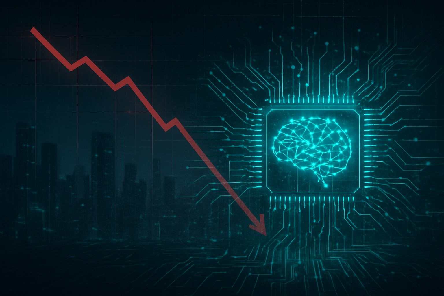
The semiconductor industry, the foundational bedrock for the burgeoning artificial intelligence revolution, is witnessing a notable trend: a surge in insider stock sales. This movement, particularly highlighted by a recent transaction from an Executive Vice President at Alpha & Omega Semiconductor (NASDAQ: AOSL), is prompting analysts and investors alike to question whether a wave of caution is sweeping through executive suites amidst the otherwise euphoric AI landscape. While often pre-planned, the cumulative volume of these sales suggests a potential hedging strategy against future uncertainties or a belief that current valuations might be reaching a peak.
On November 14, 2025, Xue Bing, the Executive Vice President of Worldwide Sales & Business Development at Alpha & Omega Semiconductor Ltd., executed a sale of 1,845 shares of AOSL common stock at $18.16 per share, totaling $33,505. This transaction, carried out under a Rule 10b5-1 trading plan established in August 2025, occurred amidst a period of significant volatility for AOSL, with the stock experiencing a substantial year-to-date decline and a recent downgrade from analysts. This individual sale, while relatively modest, contributes to a broader pattern of insider selling across the semiconductor sector, raising questions about the sustainability of current market optimism, particularly concerning the aggressive growth projections tied to AI.
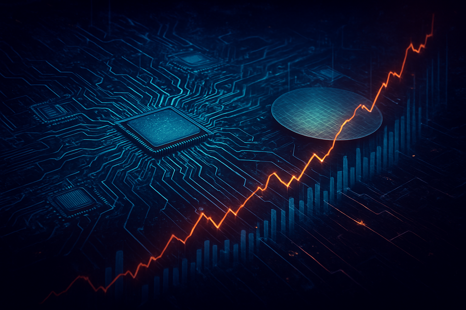
Executive Exits and Technical Trends in the Chip Sector
The recent insider transactions in the semiconductor industry paint a picture of executives de-risking their portfolios, even as public enthusiasm for AI-driven growth remains high. Xue Bing's sale at Alpha & Omega Semiconductor (NASDAQ: AOSL) on November 14, 2025, saw the EVP divest 1,845 shares for $18.16 each. While this specific sale was pre-scheduled under a Rule 10b5-1 plan, its timing coincided with a challenging period for AOSL, which had seen its stock plunge 27.6% in the week prior to November 9, 2025, and a 44.4% year-to-date drop. The company's cautious guidance and a downgrade by B.Riley, citing mixed first-quarter results and delays in its AI segment, underscore the context of this insider activity.
Beyond AOSL, the trend of insider selling is pervasive across the semiconductor landscape. Companies like ON Semiconductor (NASDAQ: ON) have seen insiders offload over 89,350 shares, totaling more than $6.3 million, over the past two years, with CEO Hassane El-Khoury making a significant sale in August 2025. Similarly, Micron Technology (NASDAQ: MU) insiders have sold over $33.79 million in shares over the preceding 12 months as of September 2025, with no reported purchases. Even at Monolithic Power Systems (NASDAQ: MPWR), CEO Michael Hsing sold 55,000 shares for approximately $28 million in November 2025. These sales, while often framed as routine liquidity management or diversification through 10b5-1 plans, collectively represent a substantial outflow of executive holdings.
This pattern differs from periods of strong bullish sentiment where insider purchases often balance or even outweigh sales, signaling deep confidence in future prospects. The current environment, marked by a high volume of sales—September 2025 recorded $691.5 million in insider sales for the sector—and a general absence of significant insider buying, suggests a more cautious stance. The technical implication is that while AI demand is undeniable, insiders might perceive current stock prices as having incorporated much of the future growth, leading them to lock in profits. The AI research community and industry experts are closely watching these movements, acknowledging the long-term potential of AI but also recognizing the potential for market corrections or a re-evaluation of high-flying valuations.
Initial reactions from the AI research community and industry experts are nuanced. While the fundamental demand for advanced semiconductors driven by AI training and inference remains robust, the pace of market capitalization growth for some chip companies has outstripped immediate revenue and earnings growth. Experts caution that while AI is a transformative force, the market's enthusiasm might be leading to a "bubble-like" environment, reminiscent of past tech booms. Insider selling, even if pre-planned, can amplify these concerns, suggesting that those closest to the operational realities and future pipelines are taking a pragmatic approach to their personal holdings.
Competitive Implications and Market Positioning in the AI Era
The recent wave of insider selling in the semiconductor sector, while not a direct indicator of AI's future, certainly casts a shadow on the near-term market confidence and carries significant competitive implications for companies deeply entrenched in the AI ecosystem. Companies like NVIDIA (NASDAQ: NVDA), a dominant force in AI accelerators, and other chipmakers supplying the foundational hardware for AI development, stand to benefit from the continued demand for high-performance computing. However, a cautious sentiment among insiders could signal a re-evaluation of the aggressive growth trajectories priced into these stocks.
For major AI labs and tech giants like Google (NASDAQ: GOOGL), Microsoft (NASDAQ: MSFT), and Amazon (NASDAQ: AMZN) that are heavily investing in AI infrastructure, the insider sales in the semiconductor sector could be a mixed signal. On one hand, it might suggest that the cost of acquiring cutting-edge chips could stabilize or even decrease if market valuations temper, potentially benefiting their massive capital expenditures. On the other hand, a broader loss of confidence in the semiconductor supply chain, even if temporary, could impact their ability to scale AI operations efficiently and cost-effectively, potentially disrupting their ambitious AI development roadmaps and service offerings.
Startups in the AI space, particularly those reliant on external funding and market sentiment, could face increased scrutiny. Investor caution stemming from insider activity in the foundational semiconductor sector might lead to tighter funding conditions or more conservative valuations for AI-focused ventures. This could significantly impact their ability to compete with well-capitalized tech giants, potentially slowing down innovation in niche areas. The competitive landscape could shift, favoring companies with robust cash flows and diversified revenue streams that can weather potential market corrections, over those solely dependent on speculative growth.
Moreover, the market positioning of various players is at stake. Companies that can demonstrate clear, tangible revenue streams from their AI-related semiconductor products, rather than just future potential, may gain an advantage. The perceived caution from insiders might force a greater emphasis on profitability and sustainable growth models, rather than solely on market share or technological breakthroughs. This could lead to a strategic repositioning across the industry, with companies focusing more on immediate returns and less on long-term, high-risk ventures if the investment climate becomes more conservative.
Broader Significance and Historical Parallels in the AI Landscape
The current trend of insider selling in the semiconductor sector, especially when juxtaposed against the backdrop of an unprecedented AI boom, holds broader significance for the entire technological landscape. It suggests a potential re-calibration of expectations within the industry, even as the transformative power of AI continues to unfold. This phenomenon fits into the broader AI landscape as a cautionary counterpoint to the prevailing narrative of limitless growth. While the fundamental drivers for AI adoption—data explosion, advanced algorithms, and increasing computational power—remain robust, the market's reaction to these drivers may be entering a more mature, and potentially more volatile, phase.
The impacts of such insider movements can be far-reaching. Beyond immediate stock price fluctuations, a sustained pattern of executive divestment can erode investor confidence, making it harder for companies to raise capital for future AI-related R&D or expansion. It could also influence mergers and acquisitions, with potential acquirers becoming more conservative in their valuations. A key concern is that this could signal an "unwind of AI mania," a phrase some market commentators are using, drawing parallels to the dot-com bubble of the late 1990s. While AI's foundational technology is far more tangible and impactful than many of the speculative ventures of that era, the rapid escalation of valuations and the sheer volume of capital pouring into the sector could be creating similar conditions of over-exuberance.
Comparisons to previous AI milestones and breakthroughs reveal a crucial difference. Earlier breakthroughs, such as the ImageNet moment or the advent of transformer models, generated excitement but were often met with a more measured market response, allowing for organic growth and deeper integration. The current AI cycle, however, has seen an almost instantaneous and exponential surge in market capitalization for companies perceived to be at the forefront. The insider selling could be interpreted as a natural, albeit concerning, response to this rapid ascent, with executives taking profits off the table before a potential market correction.
This trend forces a critical examination of the "smart money" perspective. While individual insider sales are often explained by personal financial planning, the aggregated data points to a collective sentiment. If those with the most intimate knowledge of a company's prospects and the broader industry are choosing to sell, it suggests a tempered outlook, regardless of the public narrative. This doesn't necessarily mean AI is a bubble, but rather that the market's current valuation of AI's future impact might be running ahead of current realities or potential near-term headwinds.
The Road Ahead: Navigating AI's Future Amidst Market Signals
Looking ahead, the semiconductor sector, and by extension the entire AI industry, is poised for both continued innovation and potential market adjustments. In the near term, we can expect a heightened focus on the fundamentals of semiconductor companies, with investors scrutinizing revenue growth, profitability, and tangible returns on AI-related investments more closely. The market may become less tolerant of speculative growth stories, demanding clearer pathways to commercialization and sustainable business models for AI hardware and software providers. This could lead to a period of consolidation, where companies with strong intellectual property and robust customer pipelines thrive, while those with less differentiation struggle.
Potential applications and use cases on the horizon for AI remain vast and transformative. We anticipate further advancements in specialized AI chips, such as neuromorphic processors and quantum computing components, which could unlock new levels of efficiency and capability for AI. Edge AI, enabling intelligent processing closer to the data source, will likely see significant expansion, driving demand for low-power, high-performance semiconductors. In the long term, AI's integration into every facet of industry, from healthcare to autonomous systems, will continue to fuel demand for advanced silicon, ensuring the semiconductor sector's critical role.
However, several challenges need to be addressed. The escalating cost of developing and manufacturing cutting-edge chips, coupled with geopolitical tensions affecting global supply chains, poses ongoing risks. Furthermore, the ethical implications of advanced AI and the need for robust regulatory frameworks will continue to shape public perception and market dynamics. Experts predict that while the long-term trajectory for AI and semiconductors is undeniably upward, the market may experience periods of volatility and re-evaluation. The current insider selling trend could be a precursor to such a period, prompting a more cautious, yet ultimately more sustainable, growth path for the industry.
What experts predict will happen next is a divergence within the semiconductor space. Companies that successfully pivot to highly specialized AI hardware, offering significant performance per watt advantages, will likely outperform. Conversely, those that rely on more general-purpose computing or face intense competition in commoditized segments may struggle. The market will also closely watch for any significant insider buying activity, as a strong signal of renewed confidence could help assuage current concerns. The coming months will be critical in determining whether the recent insider sales are merely routine financial planning or a harbinger of a more significant market shift.
A Prudent Pause? Assessing AI's Trajectory
The recent flurry of insider stock sales in the semiconductor sector, notably including the transaction by Alpha & Omega Semiconductor's (NASDAQ: AOSL) EVP, serves as a significant marker in the ongoing narrative of the AI revolution. The key takeaway is a nuanced message: while the long-term potential of artificial intelligence remains undisputed, the immediate market sentiment among those closest to the industry might be one of caution. These sales, even when executed under pre-planned arrangements, collectively suggest that executives are taking profits and potentially hedging against what they perceive as high valuations or impending market corrections, especially after a period of explosive growth fueled by AI hype.
This development's significance in AI history is twofold. Firstly, it highlights the increasing maturity of the AI market, moving beyond pure speculative excitement towards a more rigorous evaluation of fundamentals and sustainable growth. Secondly, it offers a crucial reminder of the cyclical nature of technological booms, urging investors and industry participants to balance enthusiasm with pragmatism. The current trend can be seen as a healthy, albeit sometimes unsettling, mechanism for the market to self-correct and re-align expectations with reality.
Looking at the long-term impact, if this cautious sentiment leads to a more measured investment environment, it could ultimately foster more sustainable innovation in AI. Companies might prioritize tangible product development and profitability over purely speculative ventures, leading to a stronger, more resilient AI ecosystem. However, a prolonged period of market skepticism could also slow down the pace of investment in foundational AI research and infrastructure, potentially impacting the speed of future breakthroughs.
In the coming weeks and months, it will be crucial to watch for several indicators. Further insider selling, particularly from key executives in leading AI chip companies, could reinforce the cautious sentiment. Conversely, any significant insider buying, especially outside of pre-planned schedules, would signal renewed confidence. Additionally, market reactions to upcoming earnings reports from semiconductor companies and AI-focused tech giants will provide further insights into whether the industry is indeed entering a phase of re-evaluation or if the current insider activity is merely a temporary blip in the relentless march of AI progress. The interplay between technological advancement and market sentiment will define the next chapter of the AI revolution.
This content is intended for informational purposes only and represents analysis of current AI developments.
TokenRing AI delivers enterprise-grade solutions for multi-agent AI workflow orchestration, AI-powered development tools, and seamless remote collaboration platforms.
For more information, visit https://www.tokenring.ai/.