As of November 2025, the relentless and ever-increasing demand from artificial intelligence (AI) applications has ignited an unprecedented era of innovation and development within the high-performance semiconductor sector. This symbiotic relationship, where AI not only consumes advanced chips but also actively shapes their design and manufacturing, is fundamentally transforming the tech industry. The global semiconductor market, propelled by this AI-driven surge, is projected to reach approximately $697 billion this year, with the AI chip market alone expected to exceed $150 billion. This isn't merely incremental growth; it's a paradigm shift, positioning AI infrastructure for cloud and high-performance computing (HPC) as the primary engine for industry expansion, moving beyond traditional consumer markets.
This "AI Supercycle" is driving a critical race for more powerful, energy-efficient, and specialized silicon, essential for training and deploying increasingly complex AI models, particularly generative AI and large language models (LLMs). The immediate significance lies in the acceleration of technological breakthroughs, the reshaping of global supply chains, and an intensified focus on energy efficiency as a critical design parameter. Companies heavily invested in AI-related chips are significantly outperforming those in traditional segments, leading to a profound divergence in value generation and setting the stage for a new era of computing where hardware innovation is paramount to AI's continued evolution.
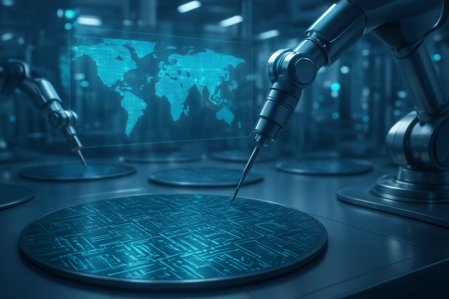
Technical Marvels: The Silicon Backbone of AI Innovation
The insatiable appetite of AI for computational power is driving a wave of technical advancements across chip architectures, manufacturing processes, design methodologies, and memory technologies. As of November 2025, these innovations are moving the industry beyond the limitations of general-purpose computing.
The shift towards specialized AI architectures is pronounced. While Graphics Processing Units (GPUs) from companies like NVIDIA (NASDAQ: NVDA) remain foundational for AI training, continuous innovation is integrating specialized AI cores and refining architectures, exemplified by NVIDIA's Blackwell and upcoming Rubin architectures. Google's (NASDAQ: GOOGL) custom-built Tensor Processing Units (TPUs) continue to evolve, with versions like TPU v5 specifically designed for deep learning. Neural Processing Units (NPUs) are becoming ubiquitous, built into mainstream processors from Intel (NASDAQ: INTC) (AI Boost) and AMD (NASDAQ: AMD) (XDNA) for efficient edge AI. Furthermore, custom silicon and ASICs (Application-Specific Integrated Circuits) are increasingly developed by major tech companies to optimize performance for their unique AI workloads, reducing reliance on third-party vendors. A groundbreaking area is neuromorphic computing, which mimics the human brain, offering drastic energy efficiency gains (up to 1000x for specific tasks) and lower latency, with Intel's Hala Point and BrainChip's Akida Pulsar marking commercial breakthroughs.
In advanced manufacturing processes, the industry is aggressively pushing the boundaries of miniaturization. While 5nm and 3nm nodes are widely adopted, mass production of 2nm technology is expected to commence in 2025 by leading foundries like TSMC (NYSE: TSM) and Samsung (KRX: 005930), offering significant boosts in speed and power efficiency. Crucially, advanced packaging has become a strategic differentiator. Techniques like 3D chip stacking (e.g., TSMC's CoWoS, SoIC; Intel's Foveros; Samsung's I-Cube) integrate multiple chiplets and High Bandwidth Memory (HBM) stacks to overcome data transfer bottlenecks and thermal issues. Gate-All-Around (GAA) transistors, entering production at TSMC and Intel in 2025, improve control over the transistor channel for better power efficiency. Backside Power Delivery Networks (BSPDN), incorporated by Intel into its 18A node for H2 2025, revolutionize power routing, enhancing efficiency and stability in ultra-dense AI SoCs. These innovations differ significantly from previous planar or FinFET architectures and traditional front-side power delivery.
AI-powered chip design is transforming Electronic Design Automation (EDA) tools. AI-driven platforms like Synopsys' DSO.ai use machine learning to automate complex tasks—from layout optimization to verification—compressing design cycles from months to weeks and improving power, performance, and area (PPA). Siemens EDA's new AI System, unveiled at DAC 2025, integrates generative and agentic AI, allowing for design suggestions and autonomous workflow optimization. This marks a shift where AI amplifies human creativity, rather than merely assisting.
Finally, memory advancements, particularly in High Bandwidth Memory (HBM), are indispensable. HBM3 and HBM3e are in widespread use, with HBM3e offering speeds up to 9.8 Gbps per pin and bandwidths exceeding 1.2 TB/s. The JEDEC HBM4 standard, officially released in April 2025, doubles independent channels, supports transfer speeds up to 8 Gb/s (with NVIDIA pushing for 10 Gbps), and enables up to 64 GB per stack, delivering up to 2 TB/s bandwidth. SK Hynix (KRX: 000660) and Samsung are aiming for HBM4 mass production in H2 2025, while Micron (NASDAQ: MU) is also making strides. These HBM advancements dramatically outperform traditional DDR5 or GDDR6 for AI workloads. The AI research community and industry experts are overwhelmingly optimistic, viewing these advancements as crucial for enabling more sophisticated AI, though they acknowledge challenges such as capacity constraints and the immense power demands.
Reshaping the Corporate Landscape: Winners and Challengers
The AI-driven semiconductor revolution is profoundly reshaping the competitive dynamics for AI companies, tech giants, and startups, creating clear beneficiaries and intense strategic maneuvers.
NVIDIA (NASDAQ: NVDA) remains the undisputed leader in the AI GPU market as of November 2025, commanding an estimated 85% to 94% market share. Its H100, Blackwell, and upcoming Rubin architectures are the backbone of the AI revolution, with the company's valuation reaching a historic $5 trillion largely due to this dominance. NVIDIA's strategic moat is further cemented by its comprehensive CUDA software ecosystem, which creates significant switching costs for developers and reinforces its market position. The company is also vertically integrating, supplying entire "AI supercomputers" and data centers, positioning itself as an AI infrastructure provider.
AMD (NASDAQ: AMD) is emerging as a formidable challenger, actively vying for market share with its high-performance MI300 series AI chips, often offering competitive pricing. AMD's growing ecosystem and strategic partnerships are strengthening its competitive edge. Intel (NASDAQ: INTC), meanwhile, is making aggressive investments to reclaim leadership, particularly with its Habana Labs and custom AI accelerator divisions. Its pursuit of the 18A (1.8nm) node manufacturing process, aiming for readiness in late 2024 and mass production in H2 2025, could potentially position it ahead of TSMC, creating a "foundry big three."
The leading independent foundries, TSMC (NYSE: TSM) and Samsung (KRX: 005930), are critical enablers. TSMC, with an estimated 90% market share in cutting-edge manufacturing, is the producer of choice for advanced AI chips from NVIDIA, Apple (NASDAQ: AAPL), and AMD, and is on track for 2nm mass production in H2 2025. Samsung is also progressing with 2nm GAA mass production by 2025 and is partnering with NVIDIA to build an "AI Megafactory" to redefine chip design and manufacturing through AI optimization.
A significant competitive implication is the rise of custom AI silicon development by tech giants. Companies like Google (NASDAQ: GOOGL), with its evolving Tensor Processing Units (TPUs) and new Arm-based Axion CPUs, Amazon Web Services (AWS) (NASDAQ: AMZN) with its Trainium and Inferentia chips, and Microsoft (NASDAQ: MSFT) with its Azure Maia 100 and Azure Cobalt 100, are all investing heavily in designing their own AI-specific chips. This strategy aims to optimize performance for their vast cloud infrastructures, reduce costs, and lessen their reliance on external suppliers, particularly NVIDIA. JPMorgan projects custom chips could account for 45% of the AI accelerator market by 2028, up from 37% in 2024, indicating a potential disruption to NVIDIA's pricing power.
This intense demand is also creating supply chain imbalances, particularly for high-end components like High-Bandwidth Memory (HBM) and advanced logic nodes. The "AI demand shock" is leading to price surges and constrained availability, with HBM revenue projected to increase by up to 70% in 2025, and severe DRAM shortages predicted for 2026. This prioritization of AI applications could lead to under-supply in traditional segments. For startups, while cloud providers offer access to powerful GPUs, securing access to the most advanced hardware can be constrained by the dominant purchasing power of hyperscalers. Nevertheless, innovative startups focusing on specialized AI chips for edge computing are finding a thriving niche.
Beyond the Silicon: Wider Significance and Societal Ripples
The AI-driven innovation in high-performance semiconductors extends far beyond technical specifications, casting a wide net of societal, economic, and geopolitical significance as of November 2025. This era marks a profound shift in the broader AI landscape.
This symbiotic relationship fits into the broader AI landscape as a defining trend, establishing AI not just as a consumer of advanced chips but as an active co-creator of its own hardware. This feedback loop is fundamentally redefining the foundations of future AI development. Key trends include the pervasive demand for specialized hardware across cloud and edge, the revolutionary use of AI in chip design and manufacturing (e.g., AI-powered EDA tools compressing design cycles), and the aggressive push for custom silicon by tech giants.
The societal impacts are immense. Enhanced automation, fueled by these powerful chips, will drive advancements in autonomous vehicles, advanced medical diagnostics, and smart infrastructure. However, the proliferation of AI in connected devices raises significant data privacy concerns, necessitating ethical chip designs that prioritize robust privacy features and user control. Workforce transformation is also a consideration, as AI in manufacturing automates tasks, highlighting the need for reskilling initiatives. Global equity in access to advanced semiconductor technology is another ethical concern, as disparities could exacerbate digital divides.
Economically, the impact is transformative. The semiconductor market is on a trajectory to hit $1 trillion by 2030, with generative AI alone potentially contributing an additional $300 billion. This has led to unprecedented investment in R&D and manufacturing capacity, with an estimated $1 trillion committed to new fabrication plants by 2030. Economic profit is increasingly concentrated among a few AI-centric companies, creating a divergence in value generation. AI integration in manufacturing can also reduce R&D costs by 28-32% and operational costs by 15-25% for early adopters.
However, significant potential concerns accompany this rapid advancement. Foremost is energy consumption. AI is remarkably energy-intensive, with data centers already consuming 3-4% of the United States' total electricity, projected to rise to 11-12% by 2030. High-performance AI chips consume between 700 and 1,200 watts per chip, and CO2 emissions from AI accelerators are forecasted to increase by 300% between 2025 and 2029. This necessitates urgent innovation in power-efficient chip design, advanced cooling, and renewable energy integration. Supply chain resilience remains a vulnerability, with heavy reliance on a few key manufacturers in specific regions (e.g., Taiwan, South Korea). Geopolitical tensions, such as US export restrictions to China, are causing disruptions and fueling domestic AI chip development in China. Ethical considerations also extend to bias mitigation in AI algorithms encoded into hardware, transparency in AI-driven design decisions, and the environmental impact of resource-intensive chip manufacturing.
Comparing this to previous AI milestones, the current era is distinct due to the symbiotic relationship where AI is an active co-creator of its own hardware, unlike earlier periods where semiconductors primarily enabled AI. The impact is also more pervasive, affecting virtually every sector, leading to a sustained and transformative influence. Hardware infrastructure is now the primary enabler of algorithmic progress, and the pace of innovation in chip design and manufacturing, driven by AI, is unprecedented.
The Horizon: Future Developments and Enduring Challenges
Looking ahead, the trajectory of AI-driven high-performance semiconductors promises both revolutionary advancements and persistent challenges. As of November 2025, the industry is poised for continuous evolution, driven by the relentless pursuit of greater computational power and efficiency.
In the near-term (2025-2030), we can expect continued refinement and scaling of existing technologies. Advanced packaging solutions like TSMC's CoWoS are projected to double in output, enabling more complex heterogeneous integration and 3D stacking. Further advancements in High-Bandwidth Memory (HBM), with HBM4 anticipated in H2 2025 and HBM5/HBM5E on the horizon, will be critical for feeding data-hungry AI models. Mass production of 2nm technology will lead to even smaller, faster, and more energy-efficient chips. The proliferation of specialized architectures (GPUs, ASICs, NPUs) will continue, alongside the development of on-chip optical communication and backside power delivery to enhance efficiency. Crucially, AI itself will become an even more indispensable tool for chip design and manufacturing, with AI-powered EDA tools automating and optimizing every stage of the process.
Long-term developments (beyond 2030) anticipate revolutionary shifts. The industry is exploring new computing paradigms beyond traditional silicon, including the potential for AI-designed chips with minimal human intervention. Neuromorphic computing, which mimics the human brain's energy-efficient processing, is expected to see significant breakthroughs. While still nascent, quantum computing holds the potential to solve problems beyond classical computers, with AI potentially assisting in the discovery of advanced materials for these future devices.
These advancements will unlock a vast array of potential applications and use cases. Data centers will remain the backbone, powering ever-larger generative AI and LLMs. Edge AI will proliferate, bringing sophisticated AI capabilities directly to IoT devices, autonomous vehicles, industrial automation, smart PCs, and wearables, reducing latency and enhancing privacy. In healthcare, AI chips will enable real-time diagnostics, advanced medical imaging, and personalized medicine. Autonomous systems, from self-driving cars to robotics, will rely on these chips for real-time decision-making, while smart infrastructure will benefit from AI-powered analytics.
However, significant challenges still need to be addressed. Energy efficiency and cooling remain paramount concerns. AI systems' immense power consumption and heat generation (exceeding 50kW per rack in data centers) demand innovations like liquid cooling systems, microfluidics, and system-level optimization, alongside a broader shift to renewable energy in data centers. Supply chain resilience is another critical hurdle. The highly concentrated nature of the AI chip supply chain, with heavy reliance on a few key manufacturers (e.g., TSMC, ASML (NASDAQ: ASML)) in geopolitically sensitive regions, creates vulnerabilities. Geopolitical tensions and export restrictions continue to disrupt supply, leading to material shortages and increased costs. The cost of advanced manufacturing and HBM remains high, posing financial hurdles for broader adoption. Technical hurdles, such as quantum tunneling and heat dissipation at atomic scales, will continue to challenge Moore's Law.
Experts predict that the total semiconductor market will surpass $1 trillion by 2030, with the AI chip market potentially reaching $500 billion for accelerators by 2028. A significant shift towards inference workloads is expected by 2030, favoring specialized ASIC chips for their efficiency. The trend of customization and specialization by tech giants will intensify, and energy efficiency will become an even more central design driver. Geopolitical influences will continue to shape policies and investments, pushing for greater self-reliance in semiconductor manufacturing. Some experts also suggest that as physical limits are approached, progress may increasingly shift towards algorithmic innovation rather than purely hardware-driven improvements to circumvent supply chain vulnerabilities.
A New Era: Wrapping Up the AI-Semiconductor Revolution
As of November 2025, the convergence of artificial intelligence and high-performance semiconductors has ushered in a truly transformative period, fundamentally reshaping the technological landscape. This "AI Supercycle" is not merely a transient boom but a foundational shift that will define the future of computing and intelligent systems.
The key takeaways underscore AI's unprecedented demand driving a massive surge in the semiconductor market, projected to reach nearly $700 billion this year, with AI chips accounting for a significant portion. This demand has spurred relentless innovation in specialized chip architectures (GPUs, TPUs, NPUs, custom ASICs, neuromorphic chips), leading-edge manufacturing processes (2nm mass production, advanced packaging like 3D stacking and backside power delivery), and high-bandwidth memory (HBM4). Crucially, AI itself has become an indispensable tool for designing and manufacturing these advanced chips, significantly accelerating development cycles and improving efficiency. The intense focus on energy efficiency, driven by AI's immense power consumption, is also a defining characteristic of this era.
This development marks a new epoch in AI history. Unlike previous technological shifts where semiconductors merely enabled AI, the current era sees AI as an active co-creator of the hardware that fuels its own advancement. This symbiotic relationship creates a virtuous cycle, ensuring that breakthroughs in one domain directly propel the other. It's a pervasive transformation, impacting virtually every sector and establishing hardware infrastructure as the primary enabler of algorithmic progress, a departure from earlier periods dominated by software and algorithmic breakthroughs.
The long-term impact will be characterized by relentless innovation in advanced process nodes and packaging technologies, leading to increasingly autonomous and intelligent semiconductor development. This trajectory will foster advancements in material discovery and enable revolutionary computing paradigms like neuromorphic and quantum computing. Economically, the industry is set for sustained growth, while societally, these advancements will enable ubiquitous Edge AI, real-time health monitoring, and enhanced public safety. The push for more resilient and diversified supply chains will be a lasting legacy, driven by geopolitical considerations and the critical importance of chips as strategic national assets.
In the coming weeks and months, several critical areas warrant close attention. Expect further announcements and deployments of next-generation AI accelerators (e.g., NVIDIA's Blackwell variants) as the race for performance intensifies. A significant ramp-up in HBM manufacturing capacity and the widespread adoption of HBM4 will be crucial to alleviate memory bottlenecks. The commencement of mass production for 2nm technology will signal another leap in miniaturization and performance. The trend of major tech companies developing their own custom AI chips will intensify, leading to greater diversity in specialized accelerators. The ongoing interplay between geopolitical factors and the global semiconductor supply chain, including export controls, will remain a critical area to monitor. Finally, continued innovation in hardware and software solutions aimed at mitigating AI's substantial energy consumption and promoting sustainable data center operations will be a key focus. The dynamic interaction between AI and high-performance semiconductors is not just shaping the tech industry but is rapidly laying the groundwork for the next generation of computing, automation, and connectivity, with transformative implications across all aspects of modern life.
This content is intended for informational purposes only and represents analysis of current AI developments.
TokenRing AI delivers enterprise-grade solutions for multi-agent AI workflow orchestration, AI-powered development tools, and seamless remote collaboration platforms.
For more information, visit https://www.tokenring.ai/.