Tag: AMD

  • The New Gatekeeper of AI: ASE Technology Signals the Chiplet Era with Record $7 Billion 2026 CapEx Plan

    The New Gatekeeper of AI: ASE Technology Signals the Chiplet Era with Record $7 Billion 2026 CapEx Plan

    KAOHSIUNG, TAIWAN — In a move that underscores the physical infrastructure demands of the artificial intelligence revolution, ASE Technology Holding Co., Ltd. (NYSE:ASX) has announced a staggering $7 billion capital expenditure plan for 2026. The record-breaking investment, representing a 27% increase over its 2025 budget, marks a strategic pivot for the world’s largest outsourced semiconductor assembly and test (OSAT) provider as it positions itself as the "capacity gatekeeper" for the next generation of AI silicon.

    The announcement comes at a critical juncture for the industry. As leading-edge chip design hits the physical limits of traditional monolith fabrication, the focus has shifted toward advanced packaging—the process of combining multiple smaller "chiplets" into a single, high-performance unit. By committing $7 billion to expand its facilities in Taiwan and Malaysia, ASE is betting that the future of AI lies not just in how transistors are made, but in how they are interconnected and cooled.

    The Technical Frontier: Beyond Moore’s Law with VIPack and FOCoS

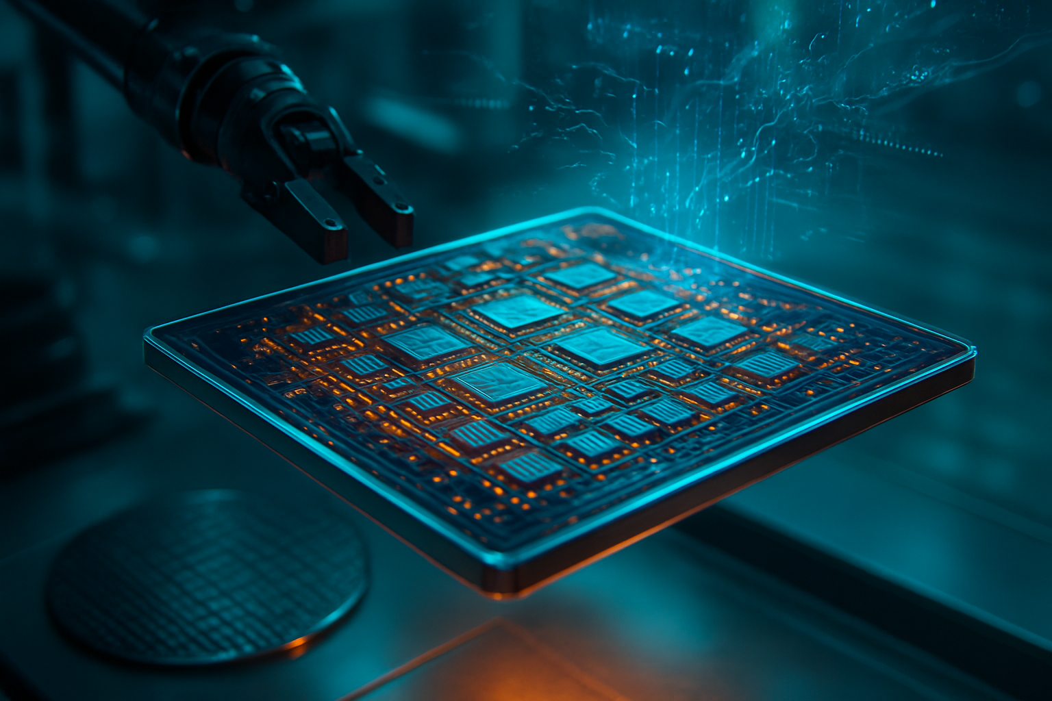
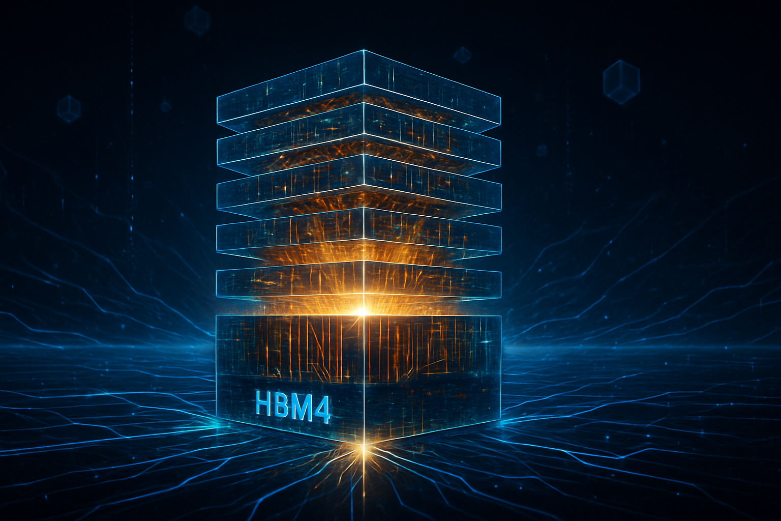
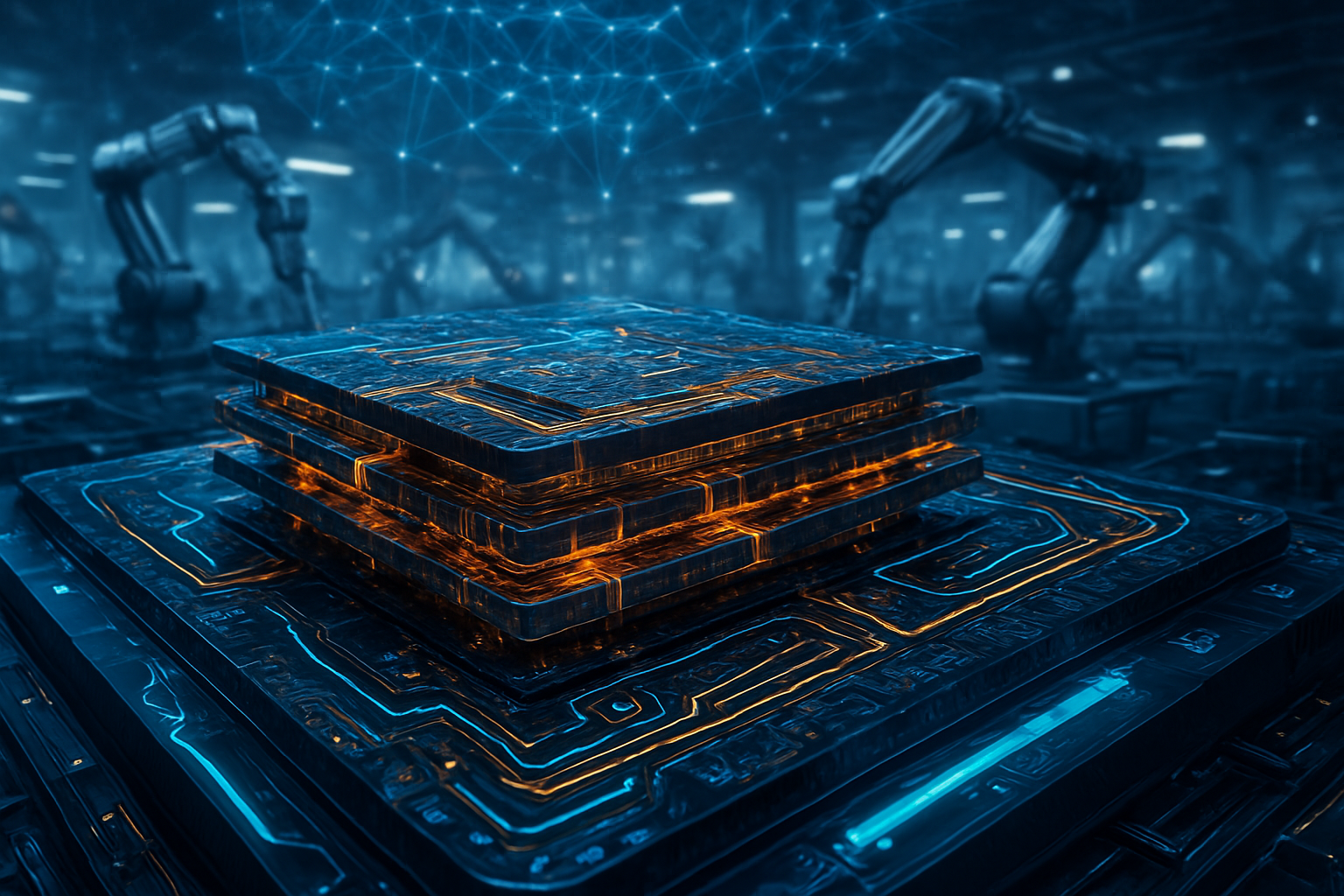
    At the heart of ASE’s 2026 expansion is a suite of proprietary technologies designed to handle the "explosive" complexity of AI processors. The investment targets the mass-scale rollout of the VIPack™ platform, which utilizes Fan-Out Chip-on-Substrate (FOCoS) and "Bridge" technologies. Unlike previous generations of packaging that relied on simple wire bonding, FOCoS-Bridge allows for silicon bridges to connect chiplets with a density nearly 200 times higher than traditional organic packages. This is essential for the low-latency communication required between high-bandwidth memory (HBM) and GPU cores found in the latest accelerators from NVIDIA (NASDAQ:NVDA) and AMD (NASDAQ:AMD).

    Furthermore, a significant portion of the $7 billion is dedicated to addressing the "thermal bottleneck" of AI hardware. As modern AI server racks now consume upwards of 120kW, ASE’s upcoming K28 Smart Factory in Kaohsiung is being engineered to integrate liquid cooling and microfluidic channels directly into the package. Technical experts from firms like TechInsights have noted that this shift toward "thermal-aware packaging" is a radical departure from previous air-cooled standards. Additionally, ASE is scaling its "PowerSiP" technology, which integrates power delivery circuits within the package to reduce energy loss by up to 50%—a critical requirement as chips move toward sub-1nm equivalent performance levels.

    Market Dynamics: Pricing Power and the "Second Supply Chain"

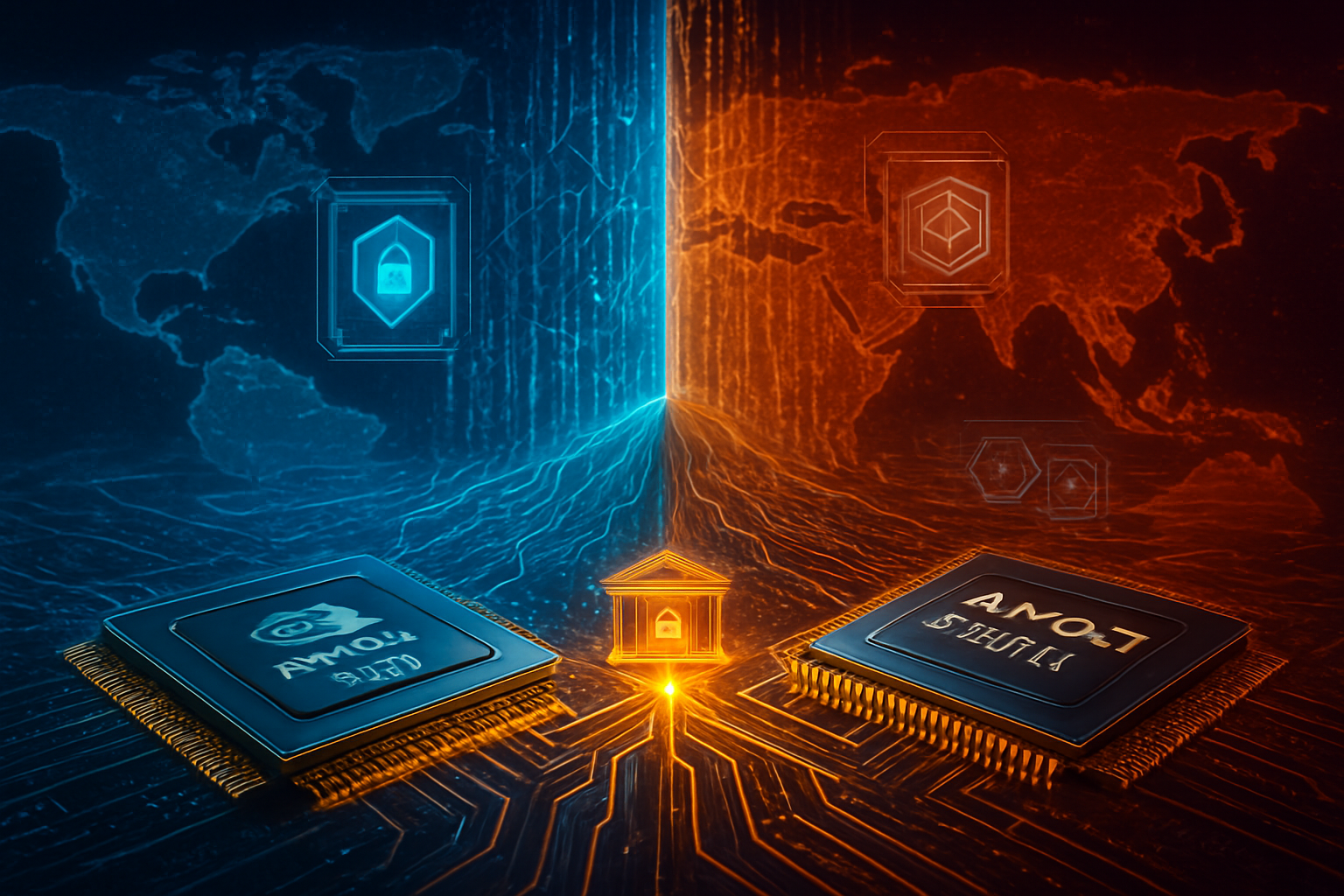
    The financial scale of this CapEx plan has sent ripples through the semiconductor market, with analysts from Morgan Stanley and Goldman Sachs identifying a structural shift in the industry's power balance. For the first time in decades, OSAT providers like ASE are wielding significant pricing power, with reports indicating ASE will raise backend packaging prices by 5% to 20% in 2026. This price hike is driven by a chronic supply-demand gap, where even the massive internal capacity of Taiwan Semiconductor Manufacturing Co. (NYSE:TSM) cannot meet the global demand for CoWoS (Chip-on-Wafer-on-Substrate) packaging.

    By tripling its "CoWoS-equivalent" capacity to 25,000 wafers per month, ASE is effectively becoming the indispensable "second supply chain" for the world's tech giants. While competitors like Amkor Technology (NASDAQ:AMKR) and Intel (NASDAQ:INTC) are also expanding their advanced packaging footprints, ASE’s 44.6% market share and its "dual-engine" growth model—leveraging both its Taiwan hubs and a massive 3.4 million square foot expansion in Penang, Malaysia—provide a strategic advantage. This geographic diversification is particularly attractive to hyperscalers like Amazon and Google, who are increasingly seeking supply chain resilience amid geopolitical tensions in the Taiwan Strait.

    The Chiplet Revolution: Redefining the Broader AI Landscape

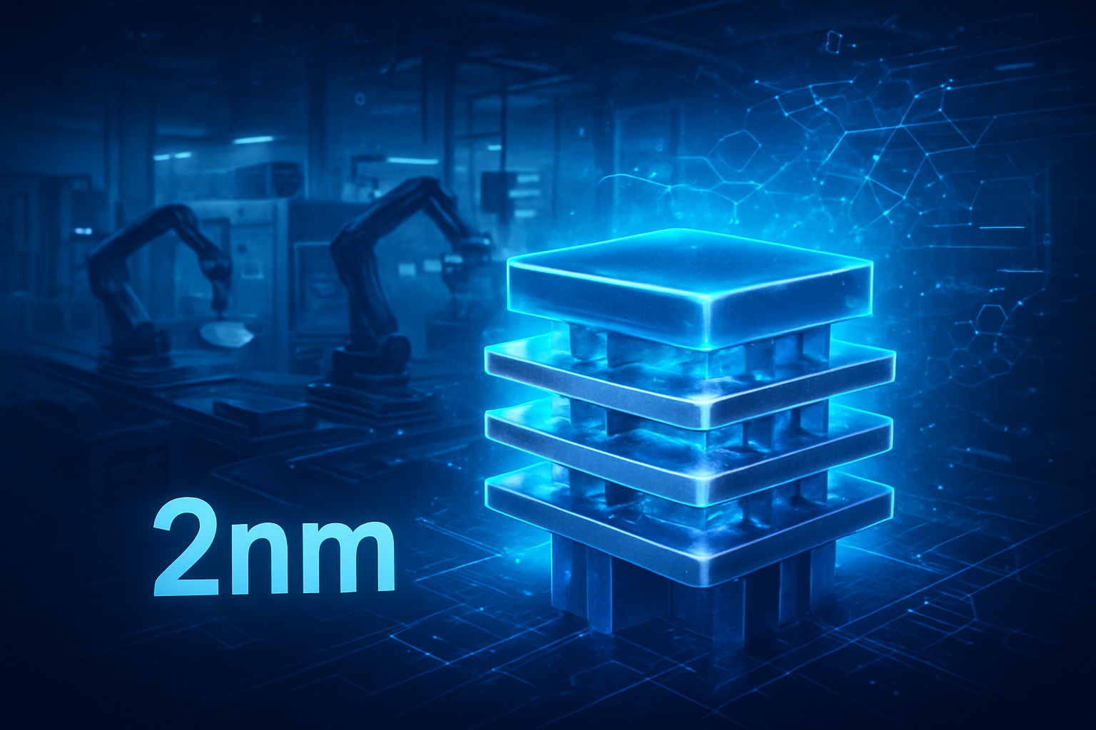
    ASE’s massive investment serves as the loudest signal yet that the "Chiplet Era" has arrived. For decades, Moore’s Law was driven by shrinking transistors on a single piece of silicon. Today, that progress has slowed and become prohibitively expensive. The industry has entered what experts call the "More than Moore" phase, where the integration of heterogeneous components—CPUs, GPUs, and specialized AI NPU chiplets—becomes the primary driver of performance gains. ASE’s $7 billion bet confirms that advanced packaging is no longer a "backend" afterthought but the very frontier of semiconductor innovation.

    This development also highlights the shifting landscape of global AI sovereignty. By expanding its Malaysian facilities alongside its Taiwan strongholds, ASE is facilitating a globalized manufacturing model that can survive localized disruptions. However, this transition is not without concerns. The reliance on advanced packaging creates new vulnerabilities, particularly regarding the supply of specialized ABF substrates and the rising cost of the high-purity metals required for 3D stacking. Much like the wafer shortages of 2021, the industry now faces a potential "packaging crunch" that could gate the speed of AI deployment for years to come.

    Looking Ahead: Co-Packaged Optics and the 2027 Horizon

    The 2026 expansion is likely only the beginning of a decade-long infrastructure cycle. Looking toward 2027 and 2028, ASE has already begun teasing the integration of Co-Packaged Optics (CPO). This technology moves optical engines directly onto the package substrate, replacing copper wires with light-based communication to further reduce the massive power consumption of AI data centers. Experts predict that as AI models continue to scale in parameter count, CPO will become a mandatory requirement for the networking fabric that connects thousands of GPUs.

    Near-term challenges remain, particularly in achieving high yields for vertically stacked 3D architectures. While 2.5D packaging (placing chips side-by-side) is maturing, true 3D stacking (placing chips on top of each other) remains a high-risk, high-reward endeavor due to the extreme heat generated in the center of the stack. ASE’s investment in "Smart Factories" and AI-driven quality control is intended to mitigate these risks, but the learning curve for these next-generation facilities will be steep as they begin trial production in late 2026.

    Conclusion: The Physical Foundation of Intelligence

    ASE Technology’s record $7 billion CapEx plan for 2026 represents a watershed moment in the history of artificial intelligence. It marks the point where the industry’s greatest bottleneck shifted from the design of AI algorithms to the physical assembly of the hardware that runs them. By doubling its leading-edge packaging revenue and aggressively expanding its global footprint, ASE is cementing its role as the essential partner for every major player in the AI ecosystem.

    In the coming weeks and months, the industry will be watching for the first equipment move-ins at the K28 facility in Kaohsiung and further details on the "FOPLP" (Fan-Out Panel Level Packaging) lines designed to bring economies of scale to massive AI chips. As 2026 unfolds, ASE’s ability to execute this $7 billion expansion will largely determine the pace at which the next generation of AI breakthroughs can be delivered to the world.


    This content is intended for informational purposes only and represents analysis of current AI developments.

    TokenRing AI delivers enterprise-grade solutions for multi-agent AI workflow orchestration, AI-powered development tools, and seamless remote collaboration platforms.
    For more information, visit https://www.tokenring.ai/.

  • AMD Shatters Records as AI Strategy Pivots to Rack-Scale Dominance: The ‘Turin’ and ‘Instinct’ Era Begins

    AMD Shatters Records as AI Strategy Pivots to Rack-Scale Dominance: The ‘Turin’ and ‘Instinct’ Era Begins

    Advanced Micro Devices, Inc. (NASDAQ:AMD) has officially crossed a historic threshold, reporting a record-shattering fourth quarter for 2025 that cements its position as the premier alternative to Nvidia in the global AI arms race. With total quarterly revenue reaching $10.27 billion—a 34% increase year-over-year—the company’s strategic pivot toward a "data center first" model has reached a critical mass. For the first time, AMD’s Data Center segment accounts for more than half of its total revenue, driven by an insatiable demand for its Instinct MI300 and MI325X GPUs and the rapid adoption of its 5th Generation EPYC "Turin" processors.

    The announcement, delivered on February 3, 2026, signals a definitive end to the era of singular dominance in AI hardware. While Nvidia remains a formidable leader, AMD’s performance suggests that the market’s thirst for high-memory AI silicon and high-throughput CPUs is allowing the Santa Clara-based chipmaker to capture significant territory. By exceeding its own aggressive AI GPU revenue forecasts—hitting over $6.5 billion for the full year 2025—AMD has proven it can execute at a scale previously thought impossible for any competitor in the generative AI era.

    Technical Superiority in Memory and Compute Density

    AMD’s current strategy is built on a "memory-first" philosophy that targets the primary bottleneck of large language model (LLM) training and inference. The newly detailed Instinct MI355X (part of the MI350 series) based on the CDNA 4 architecture represents a massive technical leap. Built on a cutting-edge 3nm process, the MI355X boasts a staggering 288GB of HBM3e memory and 8.0 TB/s of memory bandwidth. To put this in perspective, Nvidia’s (NASDAQ:NVDA) Blackwell B200 offers approximately 192GB of memory. This capacity allows AMD’s silicon to host a 520-billion parameter model on a single GPU—a task that typically requires multiple interconnected Nvidia chips—drastically reducing the complexity and energy cost of inference clusters.

    Furthermore, the integration of the 5th Generation EPYC "Turin" CPUs into AI servers has become a secret weapon for AMD. These processors, featuring up to 192 "Zen 5" cores, have seen the fastest adoption rate in the history of the EPYC line. In modern AI clusters, the CPU serves as the "head-node," managing data movement and complex system tasks. AMD’s Turin CPUs now power more than half of the company's total server revenue, as cloud providers find that their higher core density and energy efficiency are essential for maximizing the output of the attached GPUs.

    The technical community has also noted a significant narrowing of the software gap. With the release of ROCm 6.3, AMD has improved its software stack's compatibility with PyTorch and Triton, the frameworks most used by AI researchers. While Nvidia's CUDA remains the industry standard, the rise of "software-defined" AI infrastructure has made it easier for major players like Meta Platforms, Inc. (NASDAQ:META) and Oracle Corporation (NYSE:ORCL) to swap in AMD hardware without massive code rewrites.

    Reshaping the Competitive Landscape

    The industry implications of AMD’s Q4 results are profound, particularly for hyperscalers and AI startups seeking to lower their capital expenditure. By positioning itself as the "top alternative," AMD is successfully exerting downward pressure on AI chip pricing. Major deployments confirmed with OpenAI and Meta for Llama 4 training clusters indicate that the world’s most advanced AI labs are no longer content with a single-vendor supply chain. Oracle Cloud, in particular, has leaned heavily into AMD’s Instinct GPUs to offer more cost-effective "AI superclusters" to its enterprise customers.

    AMD’s strategic acquisition of ZT Systems has also begun to bear fruit. By integrating high-performance design services, AMD is moving away from being a mere component supplier to a "Rack-Scale" solutions provider. This directly challenges Nvidia’s highly successful GB200 NVL72 rack systems. AMD's forthcoming "Helios" platform, which utilizes the Ultra Accelerator Link (UALink) standard to connect 72 MI400 GPUs as a single unified unit, is designed to offer a more open, interoperable alternative to Nvidia’s proprietary NVLink technology.

    This shift to rack-scale systems is a tactical masterstroke. It allows AMD to capture a larger share of the total server bill of materials (BOM), including networking, cooling, and power management. For tech giants, this means a more modular and competitive market where they can mix and match high-performance components rather than being locked into a single vendor's ecosystem.

    Breaking the Monopoly: Wider Significance of AMD's Surge

    Beyond the balance sheets, AMD’s success marks a turning point in the broader AI landscape. The "Nvidia Monopoly" has been a point of concern for regulators and tech executives alike, fearing that a single point of failure or pricing control could stifle innovation. AMD’s ability to provide comparable—and in some memory-bound workloads, superior—performance at scale ensures a more resilient AI economy. The company’s focus on the FP6 precision standard (6-bit floating point) is also driving a new trend in "efficient inference," allowing models to run faster and with less power without sacrificing accuracy.

    However, this rapid expansion is not without its challenges. The energy requirements for these next-generation chips are astronomical. The MI355X can draw between 1,000W and 1,400W in liquid-cooled configurations, necessitating a complete rethink of data center power infrastructure. AMD’s commitment to advancing liquid-cooling technology alongside partners like Super Micro Computer, Inc. (NASDAQ:SMCI) will be critical in the coming years.

    Comparisons are already being drawn to the historical "CPU wars" of the early 2000s, where AMD’s Opteron chips challenged Intel’s dominance. The current "GPU wars," however, have much higher stakes. The winners will not just control the server market; they will control the fundamental compute engine of the 21st-century economy.

    The Road Ahead: MI400 and the Helios Era

    Looking toward the remainder of 2026 and into 2027, the roadmap for AMD is aggressive. The company has guided for a Q1 2026 revenue of approximately $9.8 billion, representing 32% year-over-year growth. The most anticipated event on the horizon is the full launch of the MI400 series and the Helios rack systems in the second half of 2026. These systems are projected to offer 50% higher memory bandwidth at the rack level than the current Blackwell architecture, potentially flipping the performance lead back to AMD for training the next generation of multi-trillion parameter models.

    Near-term challenges remain, particularly in navigating international trade restrictions. While AMD successfully launched the MI308 for the Chinese market, generating nearly $400 million in Q4, the ever-shifting landscape of export controls remains a wildcard. Additionally, the industry-wide transition to UALink and the Ultra Ethernet Consortium (UEC) standards will require flawless execution to ensure that AMD’s networking performance can truly match Nvidia's Spectrum-X and InfiniBand offerings.

    A New Chapter in AI History

    AMD’s Q4 2025 performance is more than just a strong earnings report; it is a declaration of a multi-polar AI world. By leveraging its strength in both high-performance CPUs and high-memory GPUs, AMD has created a unique value proposition that even Nvidia cannot replicate. The "Turin" and "Instinct" combination has proven that integrated, high-throughput compute is the key to scaling AI infrastructure.

    As we move deeper into 2026, the key metric to watch will be "time-to-deployment." If AMD can deliver its Helios racks on schedule and maintain its lead in memory capacity, it could realistically capture up to 40% of the AI data center market by 2027. For now, the momentum is undeniably in Lisa Su’s favor, and the tech world is watching closely as the next generation of AI silicon begins to ship.


    This content is intended for informational purposes only and represents analysis of current AI developments.

    TokenRing AI delivers enterprise-grade solutions for multi-agent AI workflow orchestration, AI-powered development tools, and seamless remote collaboration platforms.
    For more information, visit https://www.tokenring.ai/.

  • The Silicon Curtain: 25% Tariffs and US-China Revenue-Sharing Redefine the AI Arms Race

    The Silicon Curtain: 25% Tariffs and US-China Revenue-Sharing Redefine the AI Arms Race

    As of February 5, 2026, the global semiconductor landscape has undergone its most radical transformation in decades. Following the enactment of Presidential Proclamation 11002 in mid-January, the United States has officially implemented a dual-track economic strategy targeting advanced logic semiconductors: a 25% import tariff on top-tier AI hardware and a controversial, first-of-its-kind revenue-sharing arrangement with China. This policy, colloquially known as the "Washington Tax," marks a departure from total export bans, opting instead to monetize the flow of "controlled but accessible" compute power to the Chinese market.

    The move comes in the wake of the late-2025 "Busan Truce," a diplomatic breakthrough where the U.S. and China agreed to a fragile cessation of escalating trade hostilities. Under this new framework, the U.S. government now permits the sale of specific high-performance chips, such as the NVIDIA (NASDAQ: NVDA) H200 and AMD (NASDAQ: AMD) MI325X, to "approved customers" in China. However, this access comes at a steep price: 25% of all revenue from these transactions is redirected into the U.S. Treasury to fund domestic research and the "Project Vault" strategic semiconductor reserve.

    Technical Auditing and the Hardware Gatekeepers

    The technical implementation of this policy is as complex as its geopolitical goals. The baseline for the new "case-by-case" export category is defined by the processing power of the NVIDIA H200 and the AMD Instinct MI325X. The H200, built on the TSMC (NYSE: TSM) 4N architecture, boasts 141 GB of HBM3e memory and nearly 4 PFLOPS of FP8 performance. Its counterpart, the AMD MI325X, offers a massive 256 GB of HBM3E memory with 6.0 TB/s of bandwidth, making it a powerhouse for large-scale AI training. While these chips are elite by 2024 standards, they are now considered the "permissible ceiling" for export, as newer architectures like NVIDIA’s Blackwell and the rumored "Rubin" series remain strictly prohibited for Chinese entities.

    To ensure compliance, the U.S. Department of Commerce has mandated a "Third-Party Lab Interception" protocol. All chips destined for China must first pass through independent, government-approved laboratories for firmware auditing. These labs install specialized, tamper-resistant firmware developed in collaboration with U.S. national laboratories. This "Proof-of-Work" firmware enables real-time auditing of compute workloads to ensure the hardware is not being utilized for unauthorized military applications or state-run weapons research.

    The industry's reaction to these technical hurdles has been mixed. While researchers at major AI labs appreciate the clarity of the "case-by-case" review system—moving away from the "presumption of denial" that characterized 2024 and 2025—engineers have expressed concerns over the performance overhead introduced by the mandatory auditing firmware. Hardware enthusiasts have noted that the 1,000W TDP of the MI325X already pushes data center infrastructure to its limits, and the added layer of software monitoring only complicates the thermal management of these massive clusters.

    Market Dynamics: A Windfall for the Treasury, a Challenge for the Giants

    For industry leaders like NVIDIA (NASDAQ: NVDA) and AMD (NASDAQ: AMD), the 25% revenue-sharing fee represents a unique operational challenge. While it allows them to regain access to the lucrative Chinese market, the "Washington Tax" effectively narrows their profit margins on international sales or forces them to pass the cost onto Chinese buyers, who are already facing a domestic 50% equipment mandate. This mandate, enacted by Beijing in response to the U.S. tariffs, requires Chinese firms to source half of their hardware from domestic champions like Huawei and Biren.

    Strategic advantages are shifting toward companies that can navigate this bifurcated supply chain. NVIDIA, which has already established a robust ecosystem through its CUDA platform, remains the preferred choice for Chinese developers, even with the added tax. Meanwhile, AMD (NASDAQ: AMD) is leveraging the MI325X’s superior memory capacity to win over large-scale training projects that require massive datasets. The revenue collected by the U.S. Treasury—estimated to reach billions by the end of 2026—is already being funneled into "Project Vault," a strategic initiative to subsidize the construction of 2nm-capable fabs on U.S. soil.

    However, the 25% import tariff on these same logic chips when brought into the U.S. has created a "Buy American" incentive for domestic hyperscalers. Companies like Microsoft (NASDAQ: MSFT) and Alphabet (NASDAQ: GOOGL) are being nudged to favor chips that contribute to the "buildout of the U.S. technology supply chain." This has led to a surge in demand for domestic assembly and test facilities, providing a boost to firms involved in the reshoring movement.

    Geopolitical Friction and the Silicon Sovereignty

    The wider significance of the "Silicon Curtain" cannot be overstated. It represents the formalization of a "pay-to-play" era in global AI development. By allowing China to purchase older-generation silicon while taxing the revenue to fund American 2nm leadership, the U.S. is attempting to maintain a "two-generation lead" indefinitely. This strategy, however, has birthed the concept of "Silicon Sovereignty" in Beijing. China's response—a combination of massive state subsidies for domestic lithography and the 50% domestic mandate—suggests that the world is moving toward two entirely separate technology stacks.

    The "Busan Truce" of late 2025 was the catalyst for this arrangement, but many analysts view it as a temporary ceasefire rather than a permanent peace. The 25% fee is currently facing legal challenges in the U.S. Court of International Trade. Critics argue that the fee violates the Export Clause of the U.S. Constitution, which prohibits taxes on exports, and exceeds the authority granted under the Export Control Reform Act (ECRA). If these legal challenges succeed, the entire revenue-sharing model could collapse, potentially leading back to the total bans seen in previous years.

    Comparisons are already being made to the 1980s semiconductor friction between the U.S. and Japan, but the stakes today are significantly higher. AI compute is now viewed as a foundational resource, akin to oil or electricity. The ability of the U.S. to "tax" China’s AI progress to fund its own domestic infrastructure is a bold experiment in economic statecraft that has no historical precedent.

    Future Outlook: The Road to 2nm and Beyond

    Looking ahead, the next 18 to 24 months will be defined by the success of "Project Vault" and the U.S.-Taiwan landmark deal signed on January 15, 2026. This $250 billion investment aims to bring 2nm-capable production to U.S. soil by 2028. In the near term, we can expect NVIDIA and AMD to release "limited edition" versions of their next-gen chips that are specifically designed to meet the audit requirements of the "Washington Tax" framework, provided they remain below the prohibited performance thresholds.

    The most significant hurdle remains the legal battle over the "Washington Tax." If the U.S. Supreme Court is eventually forced to weigh in on the constitutionality of export fees, it could redefine the executive branch’s power over international trade. Furthermore, as Chinese domestic firms like Huawei close the performance gap, the value of being an "approved customer" for U.S. silicon may diminish, leading to a potential drop-off in the revenue that currently funds U.S. reshoring efforts.

    Experts predict that the "volume caps"—which limit shipments to China to 50% of U.S. domestic volume—will become the next flashpoint. As U.S. demand for AI clusters continues to skyrocket, the "ceiling" for Chinese access will rise, potentially leading to renewed concerns about the speed of China's military AI modernization.

    Summary of the New Status Quo

    The events of early 2026 have established a new reality for the AI industry. The "Silicon Curtain" is not just a barrier, but a complex economic filter designed to extract value from the global trade of intelligence. Key takeaways include:

    • The NVIDIA H200 and AMD MI325X are the current standard-bearers for sanctioned-but-taxed exports.
    • The 25% revenue-sharing fee is being used to directly fund the U.S. semiconductor reshoring movement.
    • Hardware-level auditing via firmware has become a mandatory component of international AI trade.

    As we move deeper into 2026, the industry must watch for the outcome of pending legal challenges and the progress of U.S. 2nm fab construction. The "Silicon Curtain" may have brought a temporary truce, but the race for computational supremacy remains as intense as ever.


    This content is intended for informational purposes only and represents analysis of current AI developments.

    TokenRing AI delivers enterprise-grade solutions for multi-agent AI workflow orchestration, AI-powered development tools, and seamless remote collaboration platforms.
    For more information, visit https://www.tokenring.ai/.

  • The 2nm AI War Begins: AMD’s MI400 and the Bold Strategy to Topple NVIDIA’s Throne

    The 2nm AI War Begins: AMD’s MI400 and the Bold Strategy to Topple NVIDIA’s Throne

    As of February 5, 2026, the artificial intelligence hardware race has entered a blistering new phase. Advanced Micro Devices, Inc. (NASDAQ: AMD) has officially pivoted from being a fast follower to an aggressive trendsetter with the ongoing rollout of its Instinct MI400 series. By leveraging Taiwan Semiconductor Manufacturing Company’s (NYSE: TSM) cutting-edge 2nm process node and a “memory-first” architecture, AMD is making a decisive play to dismantle the data center dominance of NVIDIA Corporation (NASDAQ: NVDA). This strategic shift, catalyzed by the success of the MI325X and the recent MI350 series, represents the most significant challenge to NVIDIA’s H100 and Blackwell dynasties to date.

    The immediate significance of this development cannot be overstated. By being the first to commit to mass-market 2nm AI accelerators, AMD is effectively leapfrogging the traditional manufacturing cadence. While NVIDIA’s upcoming “Rubin” architecture is expected to rely on a highly refined 3nm process, AMD is betting that the density and efficiency gains of 2nm, combined with massive HBM4 (High Bandwidth Memory) buffers, will make their silicon the preferred choice for the next generation of trillion-parameter frontier models. This is no longer a race of raw compute power alone; it is a battle for the memory bandwidth required to feed the increasingly hungry "agentic" AI systems that have come to define the 2026 landscape.

    The technological foundation of AMD’s current momentum began with the Instinct MI325X, a high-memory refresh that entered full availability in early 2025. Built on the CDNA 3 architecture, the MI325X addressed the industry’s most pressing bottleneck—the "memory wall." Featuring 256GB of HBM3e memory and a bandwidth of 6.0 TB/s, it offered a 25% lead over NVIDIA’s H200. This allowed researchers to run massive Large Language Models (LLMs) like Mixtral 8x7B up to 1.4x faster by keeping more of the model on a single chip, thereby drastically reducing the latency-inducing multi-node communication that plagues smaller-memory systems.

    Following this, the MI350 series, launched in late 2025, marked AMD’s transition to the 3nm process and the first implementation of CDNA 4. This generation introduced native support for FP4 and FP6 data formats—mathematical precisions that are essential for the efficient "thinking" processes of modern AI agents. The flagship MI355X pushed memory capacity to 288GB and introduced a 1,400W TDP, requiring advanced direct liquid cooling (DLC) infrastructure. These advancements were not merely incremental; AMD claimed a staggering 35x increase in inference performance over the original MI300 series, a figure that the AI research community has largely validated through independent benchmarks in early 2026.

    Now, the roadmap culminates in the MI400 series, specifically the MI455X, which utilizes the CDNA 5 architecture. Built on TSMC’s 2nm (N2) process, the MI400 integrates a massive 432GB of HBM4 memory, delivering an unprecedented 19.6 TB/s of bandwidth. To put this in perspective, the MI400 provides more memory on a single accelerator than entire server nodes did just three years ago. This technical leap is paired with the "Helios" rack-scale solution, which clusters 72 MI400 GPUs with EPYC “Venice” CPUs to deliver over 3 ExaFLOPS of tensor performance, aimed squarely at the "super-clusters" being built by hyperscalers.

    This aggressive roadmap has sent ripples through the tech ecosystem, benefiting several key players while forcing others to recalibrate. Hyperscalers like Microsoft Corporation (NASDAQ: MSFT), Meta Platforms, Inc. (NASDAQ: META), and Oracle Corporation (NYSE: ORCL) stand to benefit most, as AMD’s emergence provides them with much-needed leverage in price negotiations with NVIDIA. In late 2025, a landmark deal saw OpenAI adopt MI400 clusters for its internal training workloads, a move that provided AMD with a massive credibility boost and signaled that the software gap—once AMD's Achilles' heel—is rapidly closing.

    The competitive implications for NVIDIA are profound. While the Blackwell architecture remains a powerhouse, AMD’s lead in memory density has carved out a dominant position in the "Inference-as-a-Service" market. In this sector, the cost-per-token is the primary metric of success, and AMD’s ability to fit larger models on fewer chips gives it a distinct TCO (Total Cost of Ownership) advantage. Furthermore, AMD’s commitment to open standards like UALink and Ultra Ethernet is disrupting NVIDIA’s proprietary "walled garden" approach. By offering an alternative to NVLink and InfiniBand that doesn't lock customers into a single vendor's ecosystem, AMD is successfully appealing to startups and enterprises that are wary of vendor lock-in.

    Market positioning has shifted such that AMD now commands approximately 12% of the AI accelerator market, up from single digits just two years ago. While NVIDIA still holds the lion's share, AMD has effectively established itself as the "co-leader" in high-end AI silicon. This duopoly is driving a faster innovation cycle across the industry, as both companies are now forced to release major architectural updates on an annual basis rather than the biennial cadence of the previous decade.

    The broader significance of AMD’s 2nm jump lies in the shifting priorities of the AI landscape. For years, the industry was obsessed with "peak FLOPs"—the raw number of floating-point operations a chip could perform. However, as models have grown in complexity, the industry has realized that compute is often left idling while waiting for data to arrive from memory. AMD’s "memory-first" strategy, epitomized by the MI400's HBM4 integration, represents a fundamental realization that the path to Artificial General Intelligence (AGI) is paved with bandwidth, not just brute-force calculation.

    This development also highlights the increasing geopolitical and economic importance of the TSMC partnership. As the sole provider of 2nm capacity for these high-end chips, TSMC remains the linchpin of the global AI economy. AMD’s early reservation of 2nm capacity suggests a more assertive supply chain strategy, ensuring they are not sidelined as they were during the early 10nm and 7nm transitions. However, this reliance also raises concerns about geographic concentration and the potential for supply shocks should regional tensions in the Pacific escalate.

    Comparing this to previous milestones, the MI400’s 2nm transition is being viewed with the same weight as the shift from CPUs to GPUs for deep learning in the early 2010s. It marks the end of the "efficiency at any cost" era and the beginning of a specialized era where silicon is co-designed with specific model architectures in mind. The integration of ROCm 7.0, which now supports over 90% of the most popular AI APIs, further cements this milestone by proving that a viable software alternative to NVIDIA’s CUDA is finally a reality.

    Looking ahead, the next 12 to 24 months will be defined by the physical deployment of MI400-based "Helios" racks. We expect to see the first wave of 10-trillion parameter models trained on this hardware by early 2027. These models will likely power more sophisticated, multi-modal autonomous agents capable of long-form reasoning and complex physical task planning. The industry is also watching for the emergence of HBM5, which is already in the early R&D phases and promised to further expand the memory horizon.

    However, significant challenges remain. The power consumption of these systems is astronomical; with 1,400W+ TDPs becoming the norm, data center operators are facing a crisis of power availability and cooling. The move to 2nm offers better efficiency, but the sheer density of these chips means that liquid cooling is no longer optional—it is a requirement. Experts predict that the next major breakthrough will not be in the silicon itself, but in the power delivery and heat dissipation technologies required to keep these "artificial brains" from melting.

    In summary, AMD’s journey from the MI325X to the 2nm MI400 represents a masterclass in strategic execution. By focusing on the "memory wall" and securing early access to next-generation manufacturing, AMD has transformed from a budget alternative into a top-tier competitor that is, in several key metrics, outperforming NVIDIA. The MI400 series is a testament to the fact that the AI hardware market is no longer a one-horse race, but a high-stakes competition that is driving the entire tech industry toward AGI at an accelerated pace.

    As we move through 2026, the key developments to watch will be the real-world benchmarks of the MI455X against NVIDIA’s Rubin, and the continued adoption of the UALink open standard. For the first time in the generative AI era, the "NVIDIA tax" is under serious threat, and the beneficiaries will be the developers, researchers, and enterprises that now have a choice in how they build the future of intelligence.


    This content is intended for informational purposes only and represents analysis of current AI developments.

    TokenRing AI delivers enterprise-grade solutions for multi-agent AI workflow orchestration, AI-powered development tools, and seamless remote collaboration platforms.
    For more information, visit https://www.tokenring.ai/.

  • Intel’s Silicon Redemption: CPU Reliability Hits Parity with AMD Ahead of 18A Launch

    Intel’s Silicon Redemption: CPU Reliability Hits Parity with AMD Ahead of 18A Launch

    In a dramatic reversal of fortunes that has sent ripples through the semiconductor industry, Intel Corporation (NASDAQ: INTC) has officially closed the book on the reliability crisis that haunted its 13th and 14th Generation processors. According to 2025 year-end data from premier system builders, Intel’s hardware reliability has reached statistical parity with its primary rival, Advanced Micro Devices, Inc. (NASDAQ: AMD), effectively restoring the "Intel Inside" brand's reputation for rock-solid stability. This comeback comes at a pivotal moment as the company moves into high-volume manufacturing for its 18A process node, the cornerstone of CEO Pat Gelsinger’s ambitious turnaround strategy.

    The restoration of confidence is not merely a marketing win; it is a fundamental shift in the technical landscape of consumer and enterprise computing. For much of 2024, the "Vmin Shift" instability issues had left Intel on the defensive, forcing unprecedented warranty extensions and microcode patches. However, the release of the Core Ultra series, encompassing the Arrow Lake and Lunar Lake architectures, has proven to be the stable foundation the market demanded. With reliability concerns now largely in the rearview mirror, the industry is shifting its focus toward Intel’s upcoming 18A-based products, which represent the company’s most significant technological leap in over a decade.

    The Technical Road to Recovery: From Raptor Lake to Core Ultra

    The technical cornerstone of Intel’s reliability comeback lies in the architectural shift away from the troubled "Raptor Lake" design. According to the 2025 Reliability Report from Puget Systems, a leading high-end workstation builder, Intel’s latest Core Ultra (Arrow Lake) processors recorded an overall failure rate of just 2.49%, effectively matching the 2.52% failure rate of AMD’s Ryzen 9000 series. This marks the first time in nearly three years that Intel has held a statistical edge, however slight, in consumer-grade reliability. Specific standouts included the Intel Core Ultra 7 265K, which emerged as the most reliable consumer chip of 2025 with a failure rate of 0.77%.

    This recovery was achieved through a combination of manufacturing discipline and final legacy patches. In May 2025, Intel released the 0x12F microcode for 13th and 14th Gen systems, which addressed the final edge cases of the Vmin Shift—a phenomenon where high voltage and heat caused circuit degradation over time. More importantly, the new Arrow Lake and Lunar Lake architectures utilized a modular "tile" approach, with compute tiles manufactured on high-yield, stable processes. Falcon Northwest owner Kelt Reeves noted in late 2025 that the company experienced "zero RMA issues" with the Arrow Lake platform, a stark contrast to the doubled and tripled return rates seen during the peak of the 2024 instability crisis.

    The technical community has responded with cautious praise. Experts note that while the Core Ultra series didn't shatter performance records in every category, its focus on performance-per-watt and thermal stability has been the primary driver of its success. By prioritizing efficiency over the "push-to-the-limit" voltage curves of previous generations, Intel has re-established a predictable thermal envelope. This shift has been lauded by AI researchers and developers who require 24/7 uptime for local model training and data processing, where any hint of instability can lead to catastrophic data loss.

    Market Implications: Restoring Trust Among Tech Giants and Foundries

    The reliability turnaround has far-reaching consequences for Intel’s competitive positioning against AMD and its standing with major tech partners. Throughout 2025, the narrative of "Intel instability" acted as a major headwind for enterprise adoption. Now, with parity achieved, Intel is seeing a resurgence in the workstation and data center markets. The Intel Xeon W-2500 and W-3500 series notably recorded zero failures across major boutique builders in 2025, a statistic that has emboldened enterprise IT departments to reinvest in the Intel ecosystem.

    For Intel’s foundry business, this reliability milestone is a prerequisite for attracting external customers. Companies like Microsoft Corporation (NASDAQ: MSFT) and Amazon.com, Inc. (NASDAQ: AMZN) have already expanded their commitments to use Intel’s 18A node for custom AI accelerators, citing the company's renewed focus on hardware validation. Even Apple Inc. (NASDAQ: AAPL) has reportedly qualified Intel 18A-P for entry-level M-series chips, a move that would have been unthinkable during the height of the 2024 reliability crisis. While NVIDIA Corporation (NASDAQ: NVDA) famously bypassed 18A for its current generation due to early yield concerns, analysts suggest that Intel’s proven stability could bring the AI giant back to the table for future products.

    Strategically, this comeback allows Intel to compete on technical merit rather than crisis management. The 18A node is the first to deliver RibbonFET (Gate-All-Around) and PowerVia (backside power delivery) at scale. If Intel can maintain this reliability record while scaling 18A, it could fundamentally disrupt the current foundry dominance of TSMC. The market has begun to price in this "foundry turnaround," with Intel’s stock showing renewed resilience as the company prepares to ship its first 18A-based Panther Lake and Clearwater Forest processors.

    Wider Significance in the AI and Semiconductor Landscape

    Intel’s journey from a reliability crisis to industry-standard stability fits into a broader trend of "silicon hardening" in the AI era. As AI workloads become more intensive and pervasive, the physical limits of silicon are being pushed like never before. Intel’s struggle with Vmin Shift was a "canary in the coal mine" for the entire industry, highlighting the dangers of pursuing raw clock speed at the expense of long-term circuit health. By successfully navigating this crisis, Intel has set a new standard for transparent mitigation and architectural pivoting that other chipmakers are now closely watching.

    The comeback also signals a shift in the "5 nodes in 4 years" (5N4Y) roadmap from a desperate sprint to a sustainable marathon. The transition to 18A represents more than just a shrink in transistor size; it is a fundamental change in how chips are built and powered. Comparisons are already being made to Intel’s "Core" turnaround in 2006, which rescued the company from the thermal and performance dead-end of the Pentium 4 era. By prioritizing reliability in the lead-up to 18A, Intel is ensuring that its most advanced manufacturing technology isn't undermined by the same architectural flaws that plagued its previous generations.

    However, concerns remain regarding the "slow burn" of the legacy 13th and 14th Gen systems still in the wild. While the 2025 reports focus on new hardware, the long-term impact on Intel’s brand equity among general consumers—those not following microcode updates—remains to be seen. The hardware community’s focus on 18A yields and efficiency suggests that while the "stability" war has been won, the "efficiency" war against ARM-based competitors and AMD’s refined architectures is just beginning.

    The Future: 18A, Panther Lake, and Beyond

    Looking ahead to the remainder of 2026, Intel’s focus is squarely on the execution of its 18A high-volume manufacturing (HVM). The first wave of 18A products, including Panther Lake for mobile and desktop and Clearwater Forest for the data center, are expected to reach the market in the coming months. These chips will serve as the ultimate litmus test for Intel’s new manufacturing paradigm. Experts predict that if Panther Lake can deliver on its promised 15% performance-per-watt improvement while maintaining the reliability standards set by Arrow Lake, Intel could reclaim the performance crown it lost years ago.

    The road is not without challenges. While reliability has stabilized, yield rates for the 18A node are still being optimized. Reports indicate that 18A yields are improving by 7–8% per month, but they have not yet reached the peak profitability levels of more mature nodes. Addressing these yield challenges while simultaneously rolling out new packaging technologies like Foveros Direct will be Intel’s primary hurdle in 2026. Furthermore, the integration of 18A into the broader AI ecosystem—specifically for custom silicon customers—will require Intel to prove it can act as a world-class foundry service provider, not just a chip designer.

    A Comprehensive Wrap-Up: Intel’s New Lease on Life

    Intel’s successful navigation of its reliability crisis is a landmark moment in recent semiconductor history. By reaching parity with AMD in failure rates through the 2025 calendar year, the company has silenced critics who argued that its manufacturing woes were systemic and irreversible. The data from system builders like Puget Systems provides a clear, quantitative validation of Intel’s "Redemption Arc," transforming the Core Ultra series from a stopgap measure into a respected industry standard.

    The significance of this development cannot be overstated as the industry enters the 18A era. Intel has managed to decouple its future success from the failures of its past, entering the next generation of silicon manufacturing with a clean slate and a restored reputation. For investors and consumers alike, the message is clear: Intel is no longer in a state of crisis management; it is in a state of execution. In the coming weeks and months, the primary metric for Intel’s success will shift from "will it work?" to "how fast can it go?" as 18A products begin to flood the market.


    This content is intended for informational purposes only and represents analysis of current AI and hardware developments.

    TokenRing AI delivers enterprise-grade solutions for multi-agent AI workflow orchestration, AI-powered development tools, and seamless remote collaboration platforms.
    For more information, visit https://www.tokenring.ai/.

  • TSMC’s CoPoS: The Revolutionary Shift to Rectangular Panel Packaging

    TSMC’s CoPoS: The Revolutionary Shift to Rectangular Panel Packaging

    As the demand for generative AI training and inference reaches a fever pitch, the physical limits of semiconductor manufacturing are undergoing a radical transformation. Taiwan Semiconductor Manufacturing Co. (NYSE: TSM), the world’s most critical foundry, has officially initiated the transition to a revolutionary packaging architecture known as Chip-on-Panel-on-Substrate (CoPoS). This move marks the beginning of the end for the traditional 300mm circular silicon wafer as the primary medium for high-end AI chip assembly.

    By shifting from the century-old circular wafer format to massive 12.2 x 12.2-inch rectangular panels, TSMC is effectively rewriting the rules of chip geometry. This development is not merely a matter of shape; it is a strategic maneuver designed to break through the "reticle limit"—the physical size boundary that has constrained chip designers for decades. The move to CoPoS promises to enable AI accelerators that are multiple times larger and significantly more powerful than anything on the market today, including the current industry-leading Blackwell architecture from Nvidia (NASDAQ: NVDA).

    Redefining Geometry: The Technical Leap to 310mm Rectangular Panels

    For over twenty years, the 300mm (12-inch) circular wafer has been the gold standard for semiconductor fabrication. However, for advanced packaging techniques like CoWoS (Chip-on-Wafer-on-Substrate), the circular shape is increasingly inefficient. When rectangular AI chips are placed onto a circular wafer, a significant portion of the area near the edges—often referred to as "edge loss"—is wasted. TSMC’s CoPoS technology addresses this by utilizing a 310mm x 310mm (12.2 x 12.2 inch) rectangular panel format. This shift alone increases area utilization from approximately 57% on a circular wafer to over 87% on a square panel, drastically reducing waste and manufacturing costs.

    Beyond simple efficiency, CoPoS solves the looming "reticle limit" crisis. Traditional lithography machines are limited to exposing an area of roughly 858 square millimeters in a single pass. To create massive AI chips, manufacturers have had to "stitch" multiple reticle fields together on a silicon interposer. On a 300mm circular wafer, there is a physical ceiling to how many of these massive interposers can fit before hitting the curved edges. The CoPoS rectangular panel provides a vast, flat "backplane" that allows for interposers equivalent to 9.5 times the reticle limit. This allows for the integration of two or more 3nm compute dies alongside a staggering 12 to 16 stacks of High Bandwidth Memory (HBM4), a configuration that would be physically impossible to produce reliably on a circular wafer.

    Initial reactions from the AI research community and hardware engineers have been overwhelmingly positive, though tempered by the technical hurdles of the transition. Integrating such large, complex systems on a single panel introduces significant "warpage" (bending) and thermal management challenges. However, recent reports from TSMC’s primary packaging partner, Xintec (TPE: 6239), indicate that trial yields for the 310mm pilot lines have already reached 90%. This success has cleared the way for TSMC to begin equipment validation for mass-scale production at its new AP7 facility in Chiayi, Taiwan.

    The Nvidia Rubin Era and the Competitive Landscape

    The immediate beneficiary of this packaging revolution is Nvidia, which has reportedly selected CoPoS as the foundational technology for its upcoming "Rubin" architecture. While the current Blackwell Ultra (B200/B300) series pushes the absolute limits of wafer-based CoWoS-L packaging, the Nvidia Rubin R100 and the Rubin Ultra—slated for late 2027 and 2028—require the massive real estate of rectangular panels to accommodate their unprecedented memory bandwidth and compute density. This "anchor tenancy" by Nvidia ensures that TSMC’s massive capital expenditure into CoPoS is de-risked by a guaranteed market for the high-end chips.

    However, the shift to CoPoS is also a vital strategic move for other chip giants. Advanced Micro Devices (NASDAQ: AMD) and Broadcom (NASDAQ: AVGO) are reportedly in deep discussions with TSMC to utilize panel-level packaging for their future Instinct and custom AI silicon, respectively. For AMD, CoPoS offers a path to keep pace with Nvidia’s memory-heavy configurations, potentially allowing the future MI400 series to integrate even larger pools of HBM than previously thought possible. For Broadcom, the technology enables the creation of even more complex custom AI ASICs for hyperscalers like Google and Meta, who are desperate for larger "system-on-package" solutions to drive their next-generation large language models.

    The competitive implications extend beyond the chip designers to the foundries themselves. By pioneering CoPoS, TSMC is widening the "moat" between itself and rivals like Samsung and Intel (NASDAQ: INTC). While Intel has been a proponent of glass substrate technology and advanced packaging via its EMIB and Foveros technologies, TSMC’s move to standardized large-format rectangular panels leverages existing supply chains from the display and PCB industries, potentially giving it a cost and scaling advantage that will be difficult for competitors to replicate in the near term.

    A Fundamental Shift in the AI Scaling Paradigm

    The move to CoPoS represents a significant milestone in the broader AI landscape, signaling a pivot from transistor-level scaling to "System-on-Package" scaling. As Moore’s Law—the doubling of transistors on a single die—becomes increasingly expensive and physically difficult to maintain, the industry is looking to advanced packaging to provide the next leap in performance. CoPoS is the ultimate expression of this trend, treating the package itself as the new platform for innovation rather than just a protective shell for the silicon.

    This transition mirrors previous industry milestones, such as the shift from 200mm to 300mm wafers in the early 2000s, which radically lowered the cost of consumer electronics. However, the move to rectangular panels is arguably more significant because it changes the fundamental geometry of the semiconductor world to match the rectangular nature of the chips themselves. It also addresses environmental concerns by significantly reducing the amount of high-purity silicon wasted during the manufacturing process, a factor that is becoming increasingly important as the environmental footprint of AI infrastructure comes under scrutiny.

    There are, however, potential concerns regarding the concentration of this technology. With the AP7 facility in Chiayi serving as the primary hub for CoPoS, the global AI supply chain remains heavily dependent on a single geographic location. This has led to intensified calls for TSMC to expand its advanced packaging capabilities globally. Recent rumors suggest that TSMC may eventually repurpose parts of its Arizona expansion for CoPoS by 2028, which would mark the first time such advanced rectangular packaging technology would be available on U.S. soil.

    The Road Ahead: Glass Cores and the Feynman Generation

    Looking toward the horizon, the 310mm rectangular panel is only the first step in TSMC’s long-term roadmap. By 2028 or 2029, experts predict a transition to even larger 515mm x 510mm panels. This will coincide with the introduction of "glass-core" substrates within the CoPoS framework. Glass offers superior flatness and thermal stability compared to organic materials, allowing for even tighter interconnect densities. This will likely be the cornerstone of Nvidia’s post-Rubin architecture, currently codenamed "Feynman."

    The long-term development of CoPoS will also enable a new class of "megachips" that could power the first true Artificial General Intelligence (AGI) clusters. Instead of connecting thousands of individual chips via traditional networking, CoPoS may eventually allow for a "super-package" where dozens of compute dies and terabytes of HBM are integrated onto a single massive panel. The primary challenges remaining are the logistics of transporting such large, fragile panels and the development of new testing equipment that can handle the sheer scale of these components.

    A New Foundation for AI History

    The announcement and pilot-rollout of TSMC’s CoPoS technology in early 2026 marks a watershed moment for the semiconductor industry. It is a recognition that the circular wafer, while foundational to the first fifty years of computing, is no longer sufficient for the era of massive AI models. By embracing rectangular panel packaging, TSMC is providing the industry with the physical "runway" needed for AI accelerators to continue their exponential growth in capability.

    The key takeaway for the coming weeks and months will be the progress of equipment installation at the AP7 facility and the finalized specifications for the HBM4 interface, which will be the primary cargo for these new rectangular panels. As we watch the first CoPoS chips emerge from the pilot lines, it is clear that the future of AI is no longer bound by the circle. The transition to the square is not just a change in shape—it is the birth of a new architecture for the intelligence of tomorrow.


    This content is intended for informational purposes only and represents analysis of current AI developments.

    TokenRing AI delivers enterprise-grade solutions for multi-agent AI workflow orchestration, AI-powered development tools, and seamless remote collaboration platforms.
    For more information, visit https://www.tokenring.ai/.

  • The Great GPU War of 2026: AMD’s MI350 Series Challenges NVIDIA’s Blackwell Hegemony

    The Great GPU War of 2026: AMD’s MI350 Series Challenges NVIDIA’s Blackwell Hegemony

    As of January 2026, the artificial intelligence landscape has transitioned from a period of desperate hardware scarcity to an era of fierce architectural competition. While NVIDIA Corporation (NASDAQ: NVDA) maintained a near-monopoly on high-end AI training for years, the narrative has shifted in the enterprise data center. The arrival of the Advanced Micro Devices, Inc. (NASDAQ: AMD) Instinct MI325X and the subsequent MI350 series has created the first genuine duopoly in the AI accelerator market, forcing a direct confrontation over memory density and inference throughput.

    The immediate significance of this battle lies in the democratization of massive-scale inference. With the release of the MI350 series, built on the cutting-edge 3nm CDNA 4 architecture, AMD has effectively neutralized NVIDIA’s traditional software moat by offering raw hardware specifications—specifically in High Bandwidth Memory (HBM) capacity—that make it mathematically more efficient to run trillion-parameter models on AMD hardware. This shift has prompted major cloud providers and enterprise leaders to diversify their silicon portfolios, ending the "NVIDIA-only" era of the AI boom.

    Technical Superiority through Memory and Precision

    The technical skirmish between AMD and NVIDIA is currently centered on two critical metrics: HBM3e density and FP4 (4-bit floating point) throughput. The AMD Instinct MI350 series, headlined by the MI355X, boasts a staggering 288GB of HBM3e memory and a peak memory bandwidth of 8.0 TB/s. This allows the chip to house massive Large Language Models (LLMs) entirely within a single GPU's memory, reducing the latency-heavy data transfers between chips that plague smaller-memory architectures. In response, NVIDIA accelerated its roadmap, releasing the Blackwell Ultra (B300) series in late 2025, which finally matched AMD’s 288GB density by utilizing 12-high HBM3e stacks.

    AMD’s generational leap from the MI300 to the MI350 is perhaps the most significant in the company’s history, delivering a 35x improvement in inference performance. Much of this gain is attributed to the introduction of native FP4 support, a precision format that allows for higher throughput without a proportional loss in model accuracy. While NVIDIA’s Blackwell architecture (B200) initially set the gold standard for FP4, AMD’s MI350 has achieved parity in dense compute performance, claiming up to 20 PFLOPS of FP4 throughput. This technical parity has turned the "Instinct vs. Blackwell" debate into a question of TCO (Total Cost of Ownership) rather than raw capability.

    Industry experts initially reacted with skepticism to AMD’s aggressive roadmap, but the mid-2025 launch of the CDNA 4 architecture proved that AMD could maintain a yearly cadence to match NVIDIA’s breakneck speed. The research community has particularly praised AMD’s commitment to open standards via ROCm 7.0. By late 2025, ROCm reached feature parity with NVIDIA’s CUDA for the vast majority of PyTorch and JAX-based workloads, effectively lowering the "switching cost" for developers who were previously locked into NVIDIA’s ecosystem.

    Strategic Realignment in the Enterprise Data Center

    The competitive implications of this hardware parity are profound for the "Magnificent Seven" and emerging AI startups. For companies like Microsoft Corporation (NASDAQ: MSFT) and Meta Platforms, Inc. (NASDAQ: META), the MI350 series provides much-needed leverage in price negotiations with NVIDIA. By deploying thousands of AMD nodes, these giants have signaled that they are no longer beholden to a single vendor. This was most notably evidenced by OpenAI's landmark 2025 deal to utilize 6 gigawatts of AMD-powered infrastructure, a move that provided the MI350 series with the ultimate technical validation.

    For NVIDIA, the emergence of a potent MI350 series has forced a shift in strategy from selling individual GPUs to selling entire "AI Factories." NVIDIA's GB200 NVL72 rack-scale systems remain the industry benchmark for large-scale training due to the superior NVLink 5.0 interconnect, which offers 1.8 TB/s of chip-to-chip bandwidth. However, AMD’s acquisition of ZT Systems, completed in 2025, has allowed AMD to compete at this system level. AMD can now deliver fully integrated, liquid-cooled racks that rival NVIDIA’s DGX systems, directly challenging NVIDIA’s dominance in the plug-and-play enterprise market.

    Startups and smaller enterprise players are the primary beneficiaries of this competition. As NVIDIA and AMD fight for market share, the cost per token for inference has plummeted. AMD has aggressively marketed its MI350 chips as providing "40% more tokens-per-dollar" than the Blackwell B200. This pricing pressure has prevented NVIDIA from further expanding its already record-high margins, creating a more sustainable economic environment for companies building application-layer AI services.

    The Broader AI Landscape: From Scarcity to Scale

    This battle fits into a broader trend of "Inference-at-Scale," where the industry’s focus has shifted from training foundational models to serving them to millions of users efficiently. In 2024, the bottleneck was getting any chips at all; in 2026, the bottleneck is the power density and cooling capacity of the data center. The MI350 and Blackwell Ultra series both push the limits of power consumption, with peak TDPs reaching between 1200W and 1400W. This has sparked a massive secondary industry in liquid cooling and data center power management, as traditional air-cooled racks can no longer support these top-tier accelerators.

    The significance of the 288GB HBM3e threshold cannot be overstated. It marks a milestone where "frontier" models—those with 500 billion to 1 trillion parameters—can be served with significantly less hardware overhead. This reduces the physical footprint of AI data centers and mitigates some of the environmental concerns surrounding AI’s energy consumption, as higher memory density leads to better energy efficiency per inference task.

    However, this rapid advancement also brings concerns regarding electronic waste and the speed of depreciation. With both NVIDIA and AMD moving to annual release cycles, high-end accelerators purchased just 18 months ago are already being viewed as legacy hardware. This "planned obsolescence" at the silicon level is a new phenomenon for the enterprise data center, requiring a complete rethink of how companies amortize their massive capital expenditures on AI infrastructure.

    Looking Ahead: Vera Rubin and the MI400

    The next 12 to 24 months will see the introduction of NVIDIA’s "Vera Rubin" architecture and AMD’s Instinct MI400. Experts predict that NVIDIA will attempt to reclaim its undisputed lead by introducing even more proprietary interconnect technologies, potentially moving toward optical interconnects to overcome the physical limits of copper. NVIDIA is expected to lean heavily into its "Grace" CPU integration, pushing the Superchip model even harder to maintain a system-level advantage that AMD’s MI350, which often relies on third-party CPUs, may struggle to match.

    AMD, meanwhile, is expected to double down on its "chiplet" advantage. The MI400 is rumored to utilize an even more modular design, allowing for customizable ratios of compute to memory. This would allow enterprise customers to order "inference-heavy" or "training-heavy" versions of the same chip, a level of flexibility that NVIDIA’s more monolithic Blackwell architecture does not currently offer. The challenge for both will remain the supply chain; while HBM shortages have eased by early 2026, the sub-3nm fabrication capacity at TSMC remains a tightly contested resource.

    A New Era of Silicon Competition

    The battle between the AMD Instinct MI350 and NVIDIA Blackwell marks the end of the first phase of the AI revolution and the beginning of a mature, competitive industry. NVIDIA remains the revenue leader, holding approximately 85% of the market share, but AMD’s projected climb to a 10-12% share by mid-2026 represents a massive shift in the data center power dynamic. The "GPU War" has successfully moved the needle from theoretical performance to practical, enterprise-grade reliability and cost-efficiency.

    As we move further into 2026, the key metric to watch will be the adoption of these chips in the "sovereign AI" sector—nationalized data centers and regional cloud providers. While the US hyperscalers have led the way, the next wave of growth for both AMD and NVIDIA will come from global markets seeking to build their own independent AI infrastructure. For the first time in the AI era, those customers truly have a choice.


    This content is intended for informational purposes only and represents analysis of current AI developments.

    TokenRing AI delivers enterprise-grade solutions for multi-agent AI workflow orchestration, AI-powered development tools, and seamless remote collaboration platforms.
    For more information, visit https://www.tokenring.ai/.

  • Beyond the Shrink: How 6-Micrometer Hybrid Bonding is Resurrecting Moore’s Law for the AI Era

    Beyond the Shrink: How 6-Micrometer Hybrid Bonding is Resurrecting Moore’s Law for the AI Era

    As of early 2026, the semiconductor industry has reached a definitive turning point where the traditional method of scaling—simply making transistors smaller—is no longer the primary driver of computing power. Instead, the focus has shifted to "Advanced Packaging," a sophisticated method of stacking and connecting multiple chips to act as a single, massive processor. At the heart of this revolution is Taiwan Semiconductor Manufacturing Company (NYSE: TSM), whose System on Integrated Chips (SoIC) technology has become the industry standard for bridging the gap between theoretical chip designs and the massive computational demands of generative AI.

    The move to 6-micrometer (6µm) bond pitches represents the current "Goldilocks" zone of semiconductor manufacturing, providing the density required for next-generation AI accelerators like NVIDIA’s (NASDAQ: NVDA) upcoming Rubin architecture and AMD’s (NASDAQ: AMD) Instinct MI400 series. By utilizing hybrid bonding—a process that replaces traditional solder bumps with direct copper-to-copper connections—manufacturers are successfully bypassing the physical limits of monolithic silicon, effectively keeping Moore’s Law alive through vertical integration rather than horizontal shrinkage.

    The Technical Frontier: SoIC and the 6µm Milestone

    TSMC’s SoIC technology represents the pinnacle of 3D heterogeneous integration, specifically through its "bumpless" hybrid bonding technique known as SoIC-X. Unlike traditional 2.5D packaging, which places chips side-by-side on a silicon interposer (such as CoWoS), SoIC-X allows for logic-on-logic stacking. By reducing the bond pitch—the distance between interconnects—to 6 micrometers, TSMC has achieved a 100x increase in interconnect density compared to the 30-40µm pitches used in traditional micro-bump technologies. This leap allows for massive bandwidth between stacked dies, essentially eliminating the latency that usually occurs when data travels between different parts of a processor.

    Technical specifications for the 2026 roadmap indicate that while 6µm is the current high-volume standard, the industry is already testing 4µm and 3µm pitches for late 2026 deployments. This roadmap is critical for the integration of HBM4 (High Bandwidth Memory), which requires these ultra-fine pitches to manage the thermal and electrical signaling of 16-high memory stacks. Initial reactions from the research community have been overwhelmingly positive, with engineers noting that 6µm hybrid bonding allows them to treat separate chiplets as a single "virtual monolithic" die, granting the architectural freedom to mix and match different process nodes (e.g., a 2nm compute die on a 5nm I/O die).

    Market Dynamics: The Battle for AI Supremacy

    The shift toward high-density hybrid bonding has ignited a fierce competitive landscape among chip designers and foundries. NVIDIA (NASDAQ: NVDA) has pivoted its roadmap to take full advantage of TSMC’s SoIC, moving away from the side-by-side Blackwell designs toward the fully 3D-stacked Rubin platform. This move solidifies NVIDIA’s market positioning by allowing it to pack significantly more compute power into the same physical footprint, a necessity for the power-constrained environments of modern data centers. Meanwhile, AMD (NASDAQ: AMD) continues to leverage its early-mover advantage in 3D stacking; having pioneered SoIC with the MI300, it is now utilizing 6µm bonding in the MI400 to maintain its lead in memory capacity and bandwidth.

    However, TSMC is not the only player in this space. Intel (NASDAQ: INTC) is aggressively pushing its Foveros Direct 3D technology, which aims for sub-5µm pitches to support its 18A-PT process node. Intel’s "Clearwater Forest" Xeon processors are the first major test of this technology, positioning the company as a viable alternative for AI companies looking to diversify their supply chains. Samsung (KRX: 005930) is also a major contender with its X-Cube and SAINT platforms. Samsung's unique strategic advantage lies in its "turnkey" capability: it is currently the only company that can manufacture the HBM memory, the logic dies, and the advanced 3D packaging under one roof, potentially lowering costs for hyperscalers like Google or Meta.

    Wider Significance: A New Paradigm for Moore’s Law

    The wider significance of 6µm hybrid bonding cannot be overstated; it represents the shift from the "Era of Shrink" to the "Era of Integration." For decades, Moore's Law relied on the ability to double transistor density on a single piece of silicon every two years. As that process has become exponentially more expensive and physically difficult, advanced packaging has stepped in as the "Silicon Lego" solution. By stacking chips vertically, designers can continue to increase transistor counts without the catastrophic yield losses associated with building giant, monolithic chips.

    This development also addresses the "memory wall"—the bottleneck where processor speed outpaces the speed at which data can be fetched from memory. 3D stacking places memory directly on top of the logic, reducing the distance data must travel and significantly lowering power consumption. However, this transition brings new concerns, primarily regarding thermal management. Stacking high-performance logic dies creates "heat sandwiches" that require innovative cooling solutions, such as microfluidic cooling or advanced diamond-based thermal spreaders, to prevent the chips from throttling or failing.

    The Horizon: Glass Substrates and Sub-3µm Pitches

    Looking ahead, the industry is already identifying the next hurdles beyond 6µm bonding. The next two to three years will likely see the adoption of glass substrates to replace traditional organic materials. Glass offers superior flatness and thermal stability, which is essential as bond pitches continue to shrink toward 2µm and 1µm. Experts predict that by 2028, we will see the first "3.5D" architectures in the wild—complex systems where multiple 3D-stacked logic towers are interconnected on a glass interposer, providing a level of complexity that was unimaginable a decade ago.

    The challenges remaining are primarily economic and logistical. The equipment required for hybrid bonding, such as high-precision wafer-to-wafer aligners, is currently in short supply, and the "cleanliness" requirements for a 6µm bond are far stricter than for traditional packaging. Any microscopic dust particle can ruin a hybrid bond, leading to lower yields. As the industry moves toward these finer pitches, the role of automated inspection and AI-driven quality control will become just as important as the bonding technology itself.

    Conclusion: The 3D Future of Artificial Intelligence

    The transition to 6-micrometer hybrid bonding and TSMC’s SoIC platform marks a definitive end to the "monolithic era" of computing. As of January 30, 2026, the success of the world’s most powerful AI models is now inextricably linked to the success of 3D vertical stacking. By allowing for unprecedented interconnect density and bandwidth, advanced packaging has provided the industry with a second wind, ensuring that the computational gains required for the next phase of AI development remain achievable.

    In the coming months, keep a close eye on the production yields of NVIDIA’s Rubin and the initial benchmarks of Intel’s 18A-PT products. These will serve as the litmus test for whether hybrid bonding can be scaled to the volumes required by the insatiable AI market. While the physical limits of the transistor may be in sight, the architectural possibilities of 3D integration are just beginning to be explored. Moore’s Law isn’t dead; it has simply moved into the third dimension.


    This content is intended for informational purposes only and represents analysis of current AI developments.

    TokenRing AI delivers enterprise-grade solutions for multi-agent AI workflow orchestration, AI-powered development tools, and seamless remote collaboration platforms.
    For more information, visit https://www.tokenring.ai/.

  • Samsung Hits 70% Yield on 2nm GAA (SF2P): A Turning Point for the AI Chip Supply Chain

    Samsung Hits 70% Yield on 2nm GAA (SF2P): A Turning Point for the AI Chip Supply Chain

    As of January 30, 2026, the global semiconductor landscape is undergoing a tectonic shift. Samsung Electronics (KRX: 005930) has officially reached a critical performance and yield milestone for its 2nm (SF2P) production process, signaling a major challenge to the long-standing dominance of Taiwan Semiconductor Manufacturing Company (NYSE: TSM). Following its Q4 2025 earnings report, Samsung confirmed that its performance-optimized 2nm node, known as SF2P, has successfully hit the 70% yield threshold required for stable mass production—a feat that many industry skeptics thought would take years to master.

    This development is more than just a technical victory; it is a strategic lifeline for the world’s largest chip designers. With TSMC’s 2nm capacity currently overwhelmed by exclusive orders from high-priority clients, the emergence of a viable, high-yield alternative from Samsung provides a release valve for a supply chain that has been dangerously bottlenecked. By mastering the intricate Gate-All-Around (GAA) architecture ahead of its rivals, Samsung is positioning itself as the primary destination for the next generation of high-performance AI and mobile processors.

    Engineering the Future: The Maturity of 3rd-Gen GAA

    The SF2P node represents the second generation of Samsung’s 2nm platform, specifically optimized for high-performance computing (HPC) and premium mobile devices. Unlike traditional FinFET transistors, which hit physical scaling limits years ago, Samsung’s 2nm utilizes its proprietary Multi-Bridge Channel FET (MBCFET) architecture—a 3rd-generation evolution of GAA technology. This approach allows for a "nanosheet" design where the width of the channel can be adjusted to optimize for either extreme power efficiency or maximum performance. Compared to the first-generation SF2 node, the 2026-era SF2P delivers a 12% boost in clock speeds, a 25% improvement in power efficiency, and an 8% reduction in total die area.

    Technical experts note that Samsung’s early gamble on GAA—which it first introduced at the 3nm node while TSMC stuck with FinFET—is finally paying dividends. While competitors are only now navigating the "learning curve" of nanosheet production, Samsung has accumulated four years of telemetry data on GAA manufacturing. This experience has allowed the foundry to refine its extreme ultraviolet (EUV) lithography processes and address the "stochastic" defects that typically plague sub-3nm nodes. The result is a more uniform transistor structure that significantly reduces leakage current, a critical requirement for the power-hungry AI workloads of 2026.

    A Strategic Pivot: Qualcomm and AMD Secure Capacity

    The immediate beneficiaries of Samsung’s yield breakthrough are Qualcomm (NASDAQ: QCOM) and AMD (NASDAQ: AMD). As of late January 2026, both companies are reportedly in final negotiations to shift significant portions of their 2nm roadmap to Samsung Foundry. The move is driven by a stark reality: TSMC’s 2nm (N2) capacity is nearly 50% reserved by a single customer, leaving other tech giants fighting for leftovers and paying a "wafer premium" that has risen 50% over previous generations. Qualcomm is expected to utilize SF2P for its next-generation Snapdragon series, while AMD is eyeing the node for its "Venice" EPYC server CPUs to ensure supply stability in the face of skyrocketing enterprise demand.

    This shift represents a significant competitive disruption. For years, TSMC’s "foundry-only" model gave it a reputation for neutrality and reliability that Samsung, a conglomerate that also makes its own consumer products, struggled to match. However, the sheer scale of the AI boom has forced a "dual-sourcing" strategy among major chip designers. By offering competitive yields and more favorable pricing than TSMC, Samsung is transforming the foundry market from a monopoly into a true duopoly. Furthermore, Samsung’s massive $16.5 billion contract with Tesla (NASDAQ: TSLA) for its AI6 autonomous driving chips has served as a powerful "seal of approval," encouraging other automotive and data center players to reconsider their reliance on a single supplier.

    The "One-Stop" AI Solution and the Taylor, Texas Factor

    Samsung’s 2nm success is part of a broader "total solution" strategy that integrates logic, memory, and packaging. In January 2026, Samsung began large-scale shipments of its 12-layer HBM4 (High Bandwidth Memory), a key component for AI accelerators used by NVIDIA (NASDAQ: NVDA) and others. By offering 2nm logic manufacturing alongside HBM4 and advanced X-Cube 3D packaging, Samsung provides a vertically integrated stack that reduces latency and power consumption. This "one-stop shop" capability is something neither TSMC nor Intel (NASDAQ: INTC) can currently match with the same level of internal synchronization, making Samsung an attractive partner for startups building custom "Agentic AI" silicon.

    The geopolitical dimension of this ramp-up cannot be ignored. Samsung’s Taylor, Texas facility is now 93% complete and is transitioning to a "2nm-first" factory. With trial runs of ASML EUV lithography tools scheduled for March 2026, the Taylor fab is set to become a cornerstone of the "Made in USA" advanced chip initiative. This domestic capacity is a major selling point for U.S.-based companies like AMD and Google, who are under increasing pressure to diversify their manufacturing away from the geopolitical sensitivities of the Taiwan Strait. Samsung’s ability to hit 70% yield in its Korean facilities provides the blueprint for a rapid and successful ramp in the United States.

    Looking Ahead: The Road to 1.4nm and Backside Power

    While the industry focuses on the SF2P ramp, Samsung’s R&D teams are already moving toward the next frontier. Near-term developments include the introduction of SF2Z in 2027, which will incorporate Backside Power Delivery Network (BSPDN) technology. This innovation moves the power circuitry to the back of the wafer, freeing up the top side for more transistors and further reducing voltage drops. Beyond 2nm, the roadmap points toward the 1.4nm (SF1.4) node, where Samsung expects to apply lessons from its GAA maturity to achieve even more aggressive density gains.

    The challenge remains in maintaining these yields as the volume scales to hundreds of thousands of wafers per month. Experts predict that the next 12 months will be a "volume war" as Samsung attempts to match the total output capacity of TSMC’s sprawling "GigaFabs." Additionally, as AI models move from data centers to "on-device" edge environments, the demand for SF2P-class chips will expand into a wider variety of form factors, including wearable AR glasses and advanced robotics. The primary hurdle will be the continued availability of high-NA EUV tools and the specialized gases required for sub-2nm etching.

    A New Era for the Semiconductor Industry

    Samsung’s achievement of 70% yield on the SF2P node marks a historic comeback for the South Korean giant. After years of trailing TSMC in the transition from 7nm to 5nm and 4nm, Samsung has utilized the radical architecture shift of Gate-All-Around to leapfrog its competition in terms of manufacturing maturity. This development effectively breaks the "TSMC bottleneck," providing the global AI industry with the diversified supply chain it desperately needs to sustain its current pace of innovation.

    In the coming weeks, the industry will be watching for the official "tape-out" announcements from Qualcomm and AMD, which will confirm the first commercial products to use this new technology. The successful integration of SF2P into the global supply chain will not only redefine Samsung’s financial trajectory but will also serve as a catalyst for more affordable and efficient AI hardware worldwide. As we move deeper into 2026, the foundry race has officially been reset, and for the first time in a decade, the lead is up for grabs.


    This content is intended for informational purposes only and represents analysis of current AI and semiconductor developments.

    TokenRing AI delivers enterprise-grade solutions for multi-agent AI workflow orchestration, AI-powered development tools, and seamless remote collaboration platforms.
    For more information, visit https://www.tokenring.ai/.

  • Samsung’s HBM4 Breakthrough: NVIDIA and AMD Clearance Signals New Era in AI Memory

    Samsung’s HBM4 Breakthrough: NVIDIA and AMD Clearance Signals New Era in AI Memory

    In a decisive move that reshapes the competitive landscape of artificial intelligence infrastructure, Samsung Electronics (KRX: 005930) has officially cleared the final quality and reliability tests for its 6th-generation High Bandwidth Memory (HBM4) from both NVIDIA (NASDAQ: NVDA) and AMD (NASDAQ: AMD). As of late January 2026, this breakthrough signals a major reversal of fortune for the South Korean tech giant, which had spent much of the previous two years trailing behind its chief rival, SK Hynix (KRX: 000660), in the race to supply the memory chips essential for generative AI.

    The validation of Samsung’s HBM4 is not merely a logistical milestone; it is a technological leap that promises to unlock the next tier of AI performance. By securing approval for NVIDIA’s upcoming "Vera Rubin" platform and AMD’s MI450 accelerators, Samsung has positioned itself as a critical pillar for the 2026 AI hardware cycle. Industry insiders suggest that the successful qualification has already led to the conversion of multiple production lines at Samsung’s P4 and P5 facilities in Pyeongtaek to meet the explosive demand from hyperscalers like Google and Microsoft.

    Technical Specifications: The 11Gbps Frontier

    The defining characteristic of Samsung’s HBM4 is its unprecedented data transfer rate. While the industry standard for HBM3E hovered around 9.2 to 10 Gbps, Samsung’s latest modules have achieved stable speeds of 11.7 Gbps per pin. This 11Gbps+ threshold is achieved through the implementation of Samsung’s 6th-generation 10nm-class (1c) DRAM process. This marks the first time a memory manufacturer has successfully integrated 1c DRAM into an HBM stack, providing a 20% improvement in power efficiency and significantly higher bit density than the 1b DRAM currently utilized by competitors.

    Unlike previous generations, HBM4 features a fundamental architectural shift: the integration of a logic base die. Samsung has leveraged its unique position as the world’s only company with both leading-edge memory and foundry capabilities to produce a "turnkey" solution. Utilizing its own 4nm foundry process for the logic die, Samsung has eliminated the need to outsource to third-party foundries like TSMC. This vertical integration allows for tighter architectural optimization, superior thermal management, and a more streamlined supply chain, addressing the heat dissipation issues that have plagued high-density AI memory stacks in the past.

    Initial reactions from the AI research community and semiconductor analysts have been overwhelmingly positive. "Samsung’s move to a 4nm logic die in-house is a game-changer," noted one senior analyst at the Silicon Valley Semiconductor Institute. "By controlling the entire stack from the DRAM cells to the logic interface, they have managed to reduce latency and power draw at a level that was previously thought impossible for 12-layer and 16-layer stacks."

    Market Displacement: Closing the Gap with SK Hynix

    For the past three years, SK Hynix has enjoyed a near-monopoly on the high-end HBM market, particularly through its exclusive "One-Team" alliance with NVIDIA. However, Samsung’s late-January breakthrough has effectively ended this era of undisputed dominance. While SK Hynix still holds a projected 54% market share for 2026 due to earlier contract wins, Samsung is aggressively clawing back territory, targeting a 30% or higher share by the end of the fiscal year.

    The competitive implications for the "Big Three"—Samsung, SK Hynix, and Micron (NASDAQ: MU)—are profound. Samsung’s ability to clear tests for both NVIDIA and AMD simultaneously creates a supply cushion for AI chipmakers who have been desperate to diversify their sources. For AMD, Samsung’s HBM4 is the "secret sauce" for the MI450, allowing them to offer a competitive alternative to NVIDIA’s Vera Rubin platform in terms of raw memory bandwidth. This shift prevents a single-supplier bottleneck, which has historically inflated prices for data center operators.

    Strategic advantages are also shifting toward a multi-vendor model. Tech giants like Meta and Amazon are reportedly pivoting their procurement strategies to favor Samsung’s turnkey solution, which offers a faster time-to-market compared to the collaborative Hynix-TSMC model. This diversification is seen as a vital step in stabilizing the global AI supply chain, which remains under immense pressure as LLM (Large Language Model) training requirements continue to scale exponentially.

    Broader Significance: The Vera Rubin Era and Global Supply

    The timing of Samsung’s breakthrough is meticulously aligned with the broader AI landscape's transition to "Hyper-Scale" inference. As the industry moves toward NVIDIA’s Vera Rubin architecture, the demand for memory bandwidth has nearly doubled. A Rubin-based system equipped with eight stacks of Samsung’s HBM4 can reach an aggregate bandwidth of 22 TB/s. This allows for the real-time processing of models with tens of trillions of parameters, effectively moving the needle from "generative chat" to "autonomous reasoning agents."

    However, this milestone also brings potential concerns to the forefront. The sheer volume of capacity required for HBM4 production has led to a "cannibalization" of standard DRAM production lines. As Samsung and SK Hynix shift their focus to AI memory, prices for consumer-grade DDR5 and mobile LPDDR6 are expected to rise sharply in late 2026. This highlights a growing divide between the AI-industrial complex and the consumer electronics market, where AI-specific hardware is increasingly prioritized over general-purpose computing.

    Comparatively, this milestone is being likened to the transition from 2D to 3D NAND flash a decade ago. It represents a "point of no return" where memory is no longer a passive storage component but an active participant in the compute cycle. The integration of logic directly into the memory stack signifies the first major step toward "Processing-in-Memory" (PIM), a long-held dream of computer scientists that is finally becoming a commercial reality.

    Future Outlook: Mass Production and GTC 2026

    The immediate next step for Samsung is the official public debut of the HBM4 modules at NVIDIA GTC 2026, scheduled for March 16–19. This event is expected to feature live demonstrations of the Vera Rubin platform, with Samsung’s memory powering the world’s most advanced AI training clusters. Following the debut, full-scale mass production is slated to ramp up in the second quarter of 2026, with the first server systems reaching hyperscale customers by August.

    Looking further ahead, experts predict that Samsung will use its current momentum to fast-track the development of HBM4E (Enhanced). While HBM4 is just entering the market, the roadmap for 2027 already includes 20-layer stacks and even higher clock speeds. The challenge remains in maintaining yields; at 11.7 Gbps, the margin for error in the Through-Silicon Via (TSV) manufacturing process is razor-thin. If Samsung can maintain its current yield rates as it scales, it could potentially reclaim the title of the world’s leading HBM supplier by 2027.

    A New Chapter in the AI Memory War

    In summary, Samsung’s successful navigation of the NVIDIA and AMD qualification process marks a historic comeback. By delivering 11Gbps speeds and a vertically integrated 4nm logic die, Samsung has proved that its "all-under-one-roof" strategy is a viable—and perhaps superior—alternative to the collaborative models of its rivals. This development ensures that the AI industry has the memory bandwidth necessary to power the next generation of reasoning-capable artificial intelligence.

    In the coming weeks, the industry will be watching for the official pricing structures and the first performance benchmarks of the Vera Rubin platform at GTC 2026. While SK Hynix remains a formidable opponent with deep ties to the AI ecosystem, Samsung has officially closed the gap, turning a one-horse race into a high-speed pursuit that will define the future of computing for years to come.


    This content is intended for informational purposes only and represents analysis of current AI developments.

    TokenRing AI delivers enterprise-grade solutions for multi-agent AI workflow orchestration, AI-powered development tools, and seamless remote collaboration platforms.
    For more information, visit https://www.tokenring.ai/.