At the 2026 Consumer Electronics Show (CES) in Las Vegas, Advanced Micro Devices, Inc. (NASDAQ: AMD) officially unveiled its Ryzen AI 400 series, a breakthrough in the evolution of the “AI PC” that transitions local artificial intelligence from a luxury feature to a mainstream necessity. Codenamed "Gorgon Point," the new silicon lineup introduces the industry’s first dedicated Copilot+ desktop processors and sets a new benchmark for on-device inference efficiency. By pushing the boundaries of neural processing power, AMD is making a bold claim: the future of high-end AI development and execution no longer belongs solely to the cloud or massive server racks, but to the laptop on your desk.
The announcement marks a pivotal shift in the hardware landscape, as AMD moves beyond the niche adoption of early AI accelerators toward a "volume platform" strategy. The Ryzen AI 400 series aims to solve the latency and privacy bottlenecks that have historically plagued cloud-dependent AI services. With significant gains in NPU (Neural Processing Unit) throughput and a specialized "Halo" platform designed for extreme local workloads, AMD is positioning itself as the leader in "Sovereign AI"—the ability for individuals and enterprises to run massive, complex models entirely offline without sacrificing performance or battery life.
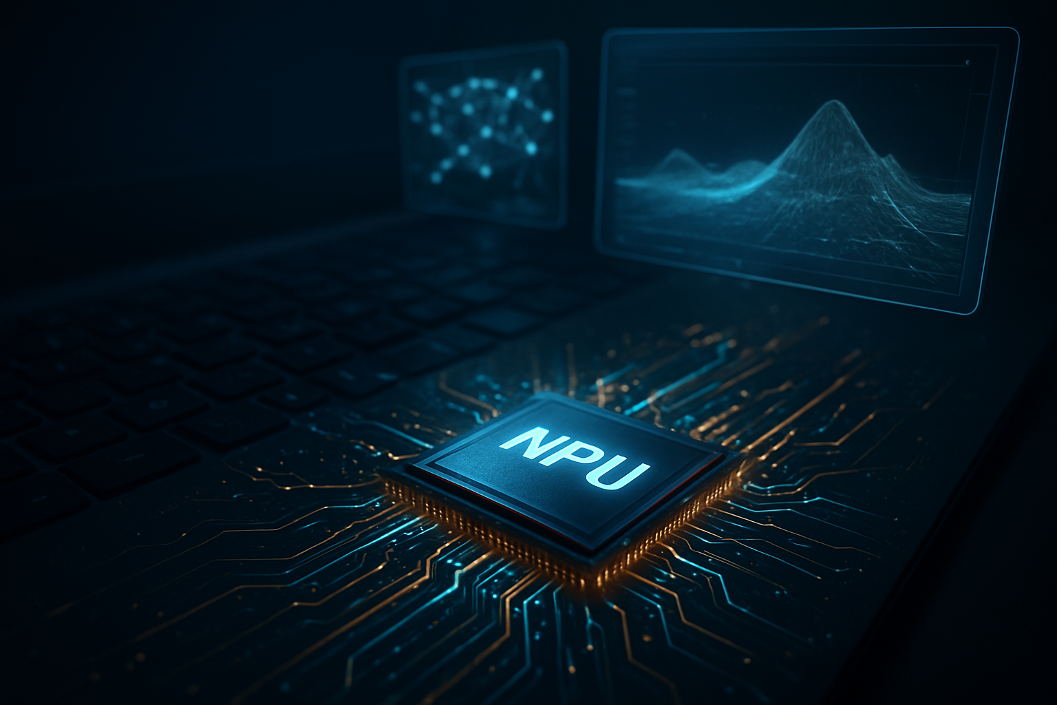
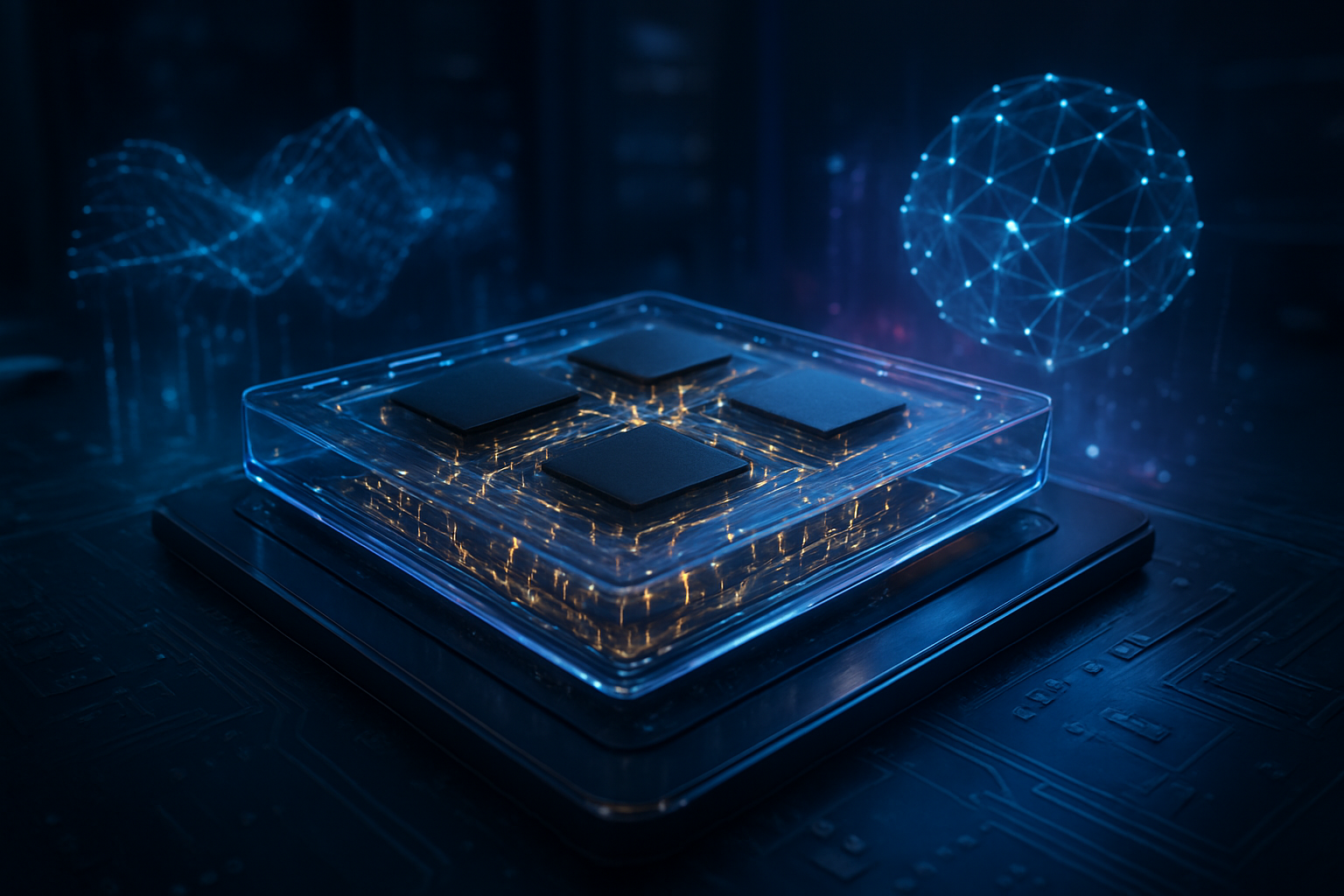
Technical Prowess: 60 TOPS and the 200-Billion Parameter Local Frontier
The Ryzen AI 400 series is built on a refined second-generation XDNA 2 architecture, paired with the proven Zen 5 and Zen 5c CPU cores on a TSMC (NYSE: TSM) 4nm process. The flagship of the mobile lineup, the Ryzen AI 9 HX 475, delivers an industry-leading 60 NPU TOPS (Trillions of Operations Per Second). This is a 20% jump over the previous generation and comfortably exceeds the 40 TOPS requirement set by Microsoft Corporation (NASDAQ: MSFT) for the Copilot+ ecosystem. To support this massive compute capability, AMD has upgraded memory support to LPDDR5X-8533 MT/s, ensuring that the high-speed data paths required for real-time generative AI remain clear and responsive.
While the standard 400 series caters to everyday productivity and creative tasks, the real showstopper at CES was the "Ryzen AI Halo" platform, utilizing the Ryzen AI Max+ silicon. In a live demonstration that stunned the audience, AMD showed the Halo platform running a 200-billion parameter large language model (LLM) locally. This feat, previously thought impossible for a consumer-grade workstation without multiple dedicated enterprise GPUs, is made possible by 128GB of high-speed unified memory. This allows the processor to handle massive datasets and complex reasoning tasks that were once the sole domain of data centers.
This technical achievement differs significantly from previous approaches, which relied on "quantization"—the process of shrinking models and losing accuracy to fit them onto consumer hardware. The Ryzen AI 400 series, particularly in its Max+ configuration, provides enough raw bandwidth and specialized NPU cycles to run high-fidelity models. Initial reactions from the AI research community have been overwhelmingly positive, with many experts noting that this level of local compute could democratize AI research, allowing developers to iterate on sophisticated models without the mounting costs of cloud API tokens.
Market Warfare: The Battle for the AI PC Crown
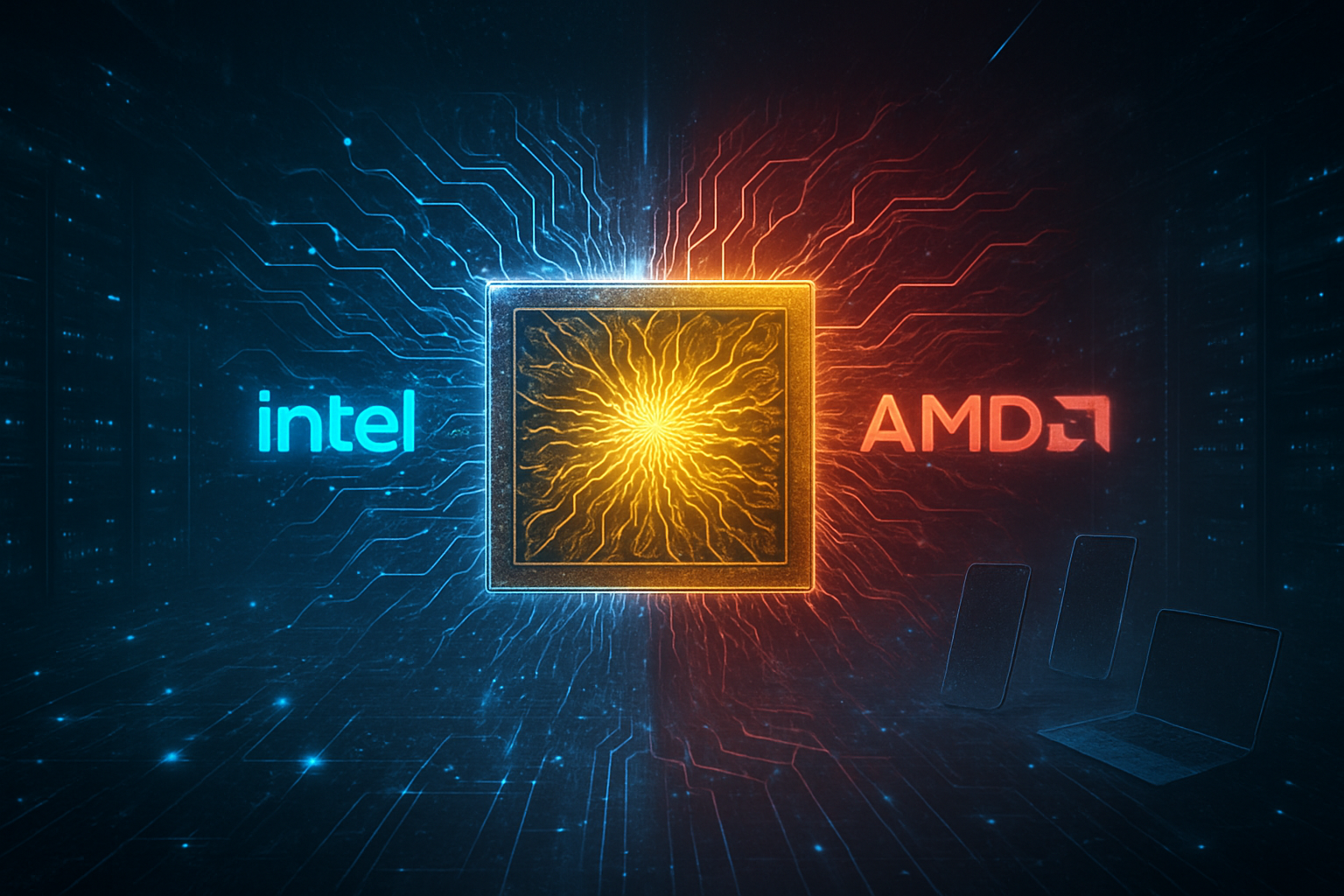
The introduction of the Ryzen AI 400 series intensifies a three-way battle for dominance in the 2026 hardware market. While Intel Corporation (NASDAQ: INTC) used CES to showcase its "Panther Lake" architecture, focusing on a 50% improvement in power efficiency and its new Xe3 "Battlemage" graphics, AMD’s strategy leans more heavily into raw AI performance and "unplugged" consistency. AMD claims a 70% improvement in performance-per-watt while running on battery compared to its predecessor, directly challenging the efficiency narrative long held by Apple and ARM-based competitors.
Qualcomm Incorporated (NASDAQ: QCOM) remains a formidable threat with its Snapdragon X2 Elite, which currently leads the market in raw NPU metrics at 80 TOPS. However, AMD’s strategic advantage lies in its x86 legacy. By bringing Copilot+ capabilities to the desktop for the first time with the Ryzen AI 400 series, AMD is securing the enterprise sector, where compatibility with legacy software and high-performance desktop workflows remains non-negotiable. This move effectively boxes out competitors who are still struggling to translate ARM efficiency into the heavy-duty desktop market.
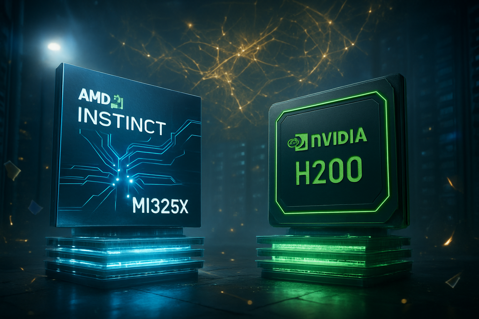
The "Ryzen AI Max+" also represents a direct challenge to NVIDIA Corporation (NASDAQ: NVDA) and its dominance in the AI workstation market. By offering a unified chip that can handle both traditional compute and massive AI inference, AMD is attempting to lure developers into its ROCm (Radeon Open Compute) software ecosystem. If AMD can convince the next generation of AI engineers that they can build, test, and deploy 200B parameter models on a single Ryzen AI-powered machine, it could significantly disrupt the sales of entry-level enterprise AI GPUs.
A Cultural Shift Toward AI Sovereignty and Privacy
Beyond the raw specifications, the Ryzen AI 400 series reflects a broader trend in the tech industry: the move toward "Sovereign AI." As concerns over data privacy, cloud security, and the environmental cost of massive data centers grow, the ability to process data locally is becoming a major selling point. For industries like healthcare, law, and finance—where data cannot leave the local network for regulatory reasons—AMD’s new chips provide a path to utilize high-end generative AI without the risks associated with third-party cloud providers.
This development follows the trajectory of the "AI PC" evolution that began in late 2023 but finally reached maturity in 2026. Earlier milestones were focused on simple background blur for video calls or basic text summarization. The 400 series, however, enables "high-level reasoning" locally. This means a laptop can now serve as a truly autonomous digital twin, capable of managing complex schedules, coding entire applications, and analyzing massive spreadsheets without ever sending a packet of data to the internet.
Potential concerns remain, particularly regarding the "AI tax" on hardware prices. As NPUs become larger and memory requirements skyrocket to support 128GB unified architectures, the cost of top-tier AI laptops is expected to rise. Furthermore, the software ecosystem must keep pace; while the hardware is now capable of running 200B parameter models, the user experience depends entirely on how effectively developers can optimize their software to leverage AMD’s XDNA 2 architecture.
The Horizon: What Comes After 60 TOPS?
Looking ahead, the Ryzen AI 400 series is just the beginning of a multi-year roadmap for AMD. Industry analysts predict that by 2027, we will see the introduction of "XDNA 3" and "Zen 6" architectures, which are expected to push NPU performance beyond the 100 TOPS mark for mobile devices. Near-term developments will likely focus on the "Ryzen AI Software" suite, with AMD expected to release more robust tools for one-click local LLM deployment, making it easier for non-technical users to host their own private AI assistants.
The potential applications are vast. In the coming months, we expect to see the rise of "Personalized Local LLMs"—AI models that are fine-tuned on a user’s specific files, emails, and voice recordings, stored and processed entirely on their Ryzen AI 400 device. Challenges remain in cooling these high-performance NPUs in thin-and-light chassis, but AMD’s move to a 4nm process and focus on "sustained unplugged performance" suggests they have a significant lead in managing the thermal realities of mobile AI.
Final Assessment: A Landmark Moment for Computing
The unveiling of the Ryzen AI 400 series at CES 2026 will likely be remembered as the moment the "AI PC" became a reality for the masses. By standardizing 60 TOPS across its stack and providing a "Halo" tier capable of running world-class AI models locally, AMD has redefined the expectations for personal computing. This isn't just a spec bump; it is a fundamental reconfiguration of where intelligence lives in the digital age.
The significance of this development in AI history cannot be overstated. We are moving from an era of "Cloud-First" AI to "Local-First" AI. In the coming weeks, as the first laptops featuring the Ryzen AI 9 HX 475 hit the shelves, the tech world will be watching closely to see if real-world performance matches the impressive CES benchmarks. If AMD’s promises of 24-hour battery life and 200B parameter local inference hold true, the balance of power in the semiconductor industry may have just shifted permanently.
This content is intended for informational purposes only and represents analysis of current AI developments.
TokenRing AI delivers enterprise-grade solutions for multi-agent AI workflow orchestration, AI-powered development tools, and seamless remote collaboration platforms.
For more information, visit https://www.tokenring.ai/.